1. Introduction
In recent years, wireless power transfer (WPT) has become increasingly popular for different applications, such as wireless charging, radio frequency identification devices (RFID), electric vehicles and implantable medical devices [
1,
2,
3,
4].
Wireless power receivers obtain power from the secondary coil of the WPT system, and the receiver achieves the conversion of alternating current to direct current (AC–DC). The direct current (DC) from the receiver is applied to different circuit blocks. The conventional receivers are usually made up of a rectifier and a regulator, which are referred to as a two-stage structure: The rectifier converts the alternating current (AC) signal to an unregulated DC signal, and the regulator realizes direct current to direct current (DC–DC) [
5]. The most common regulators are the low-dropout (LDO) and DC–DC regulators.
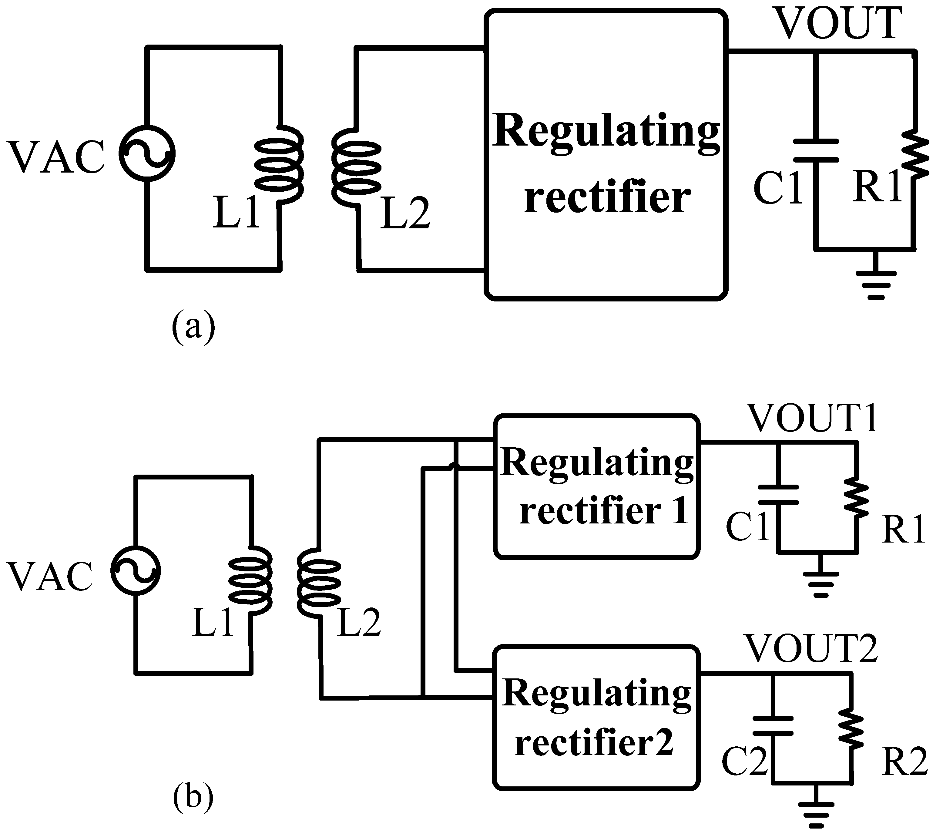
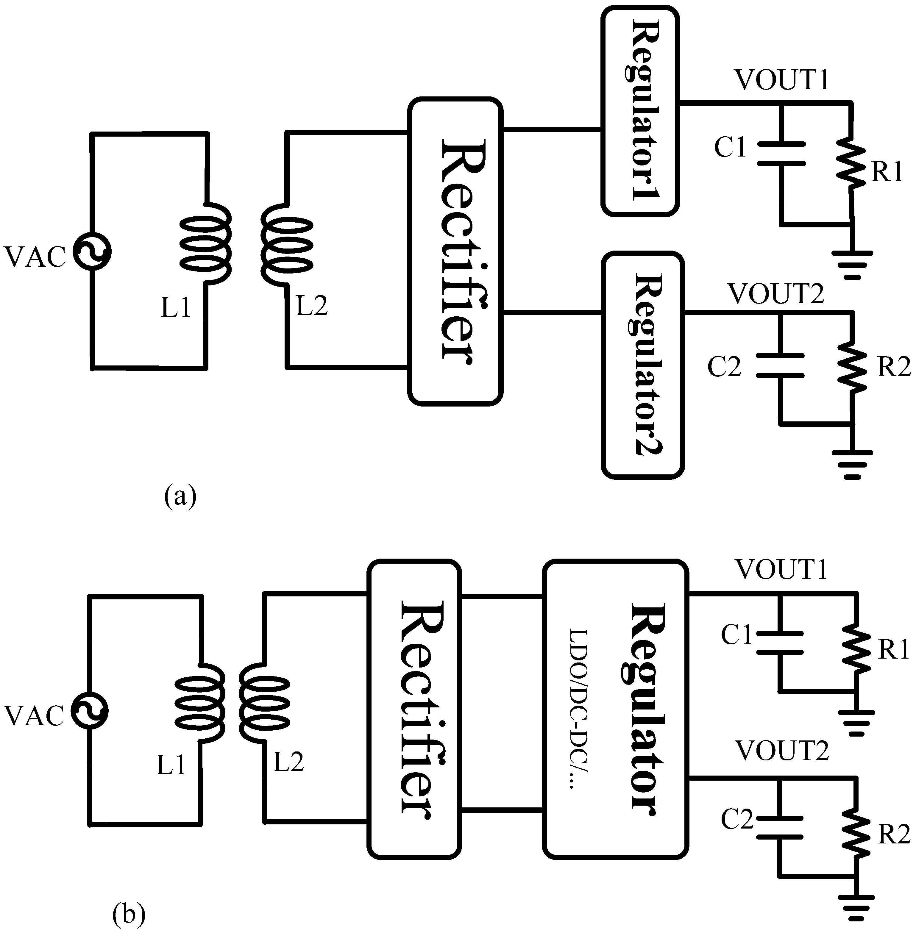
In many applications, different modules need power supplies from one system, which requires multiple output voltages from a receiver. For example, for portable solid-state drives, two different voltages are applied to the power memory circuit and the core logic circuit. It is necessary to develop multi-output receivers. Many researchers have focused on multi-output receivers, which can be realized by different methods. The multi-output regulator in [
6] adopts two separated DC–DC converters to produce two independent voltages, as shown in
Figure 1a, which uses two inductors in the footprint. The classic method for wireless power receivers to realize multi-output regulating voltages is shown in
Figure 1b [
7]. The receiver in [
7] uses a single-inductor, dual-output (SIDO) structure with only one inductor to reduce costs. However, SIDO receivers exhibit a cross-regulation phenomenon due to the sharing of power from one inductor, which means that when one output voltage changes, the other output voltage also changes [
8]. The efficiency of a two-stage receiver is shown in Equation (1); the efficiencies of both the rectifier and the regulator influence system efficiency. Additionally, the interstage loss between the rectifier and the regulator degrades the overall efficiency of the receiver, which cannot be ignored.
Single-stage receivers have been developed for higher power conversion efficiency and fewer power transistors, which combine the functions of the rectifier and the regulator and convert the input AC signal to the regulating output DC signal [
9,
10], as shown in
Figure 2a. The single-stage AC–DC converter is usually implemented in two ways: one way is by using a reconfigurable rectifier [
11], and the other way is by controlling the conduction time of power transistors to regulate the output voltage [
12,
13]. In [
9,
10], the authors focus on converting the AC signal to the regulating DC signal directly, but the structures cannot deliver different output voltages.
In reality, some situations need single-stage multi-output receivers for the advantage of not needing an inductor. For example, for implanted medical devices, different voltages are needed to supply digital and analog modules; due to the special implanted environment, a small chip size is required.
Figure 2b presents a single-stage dual-output receiver, which is realized by two self-regulating rectifiers linking with the same secondary coil in parallel [
14]. However, cross-regulation occurs due to the shared inductor. In [
8,
9,
13], the authors realize dual-output receivers in one stage, which adopts different controllers to regulate different output voltages simultaneously. In [
15], a single-stage dual-output wireless power receiver with ten power transistors is described. In [
13], an AC–DC single-stage receiver with six power transistors is described. Both receivers in [
13,
15] occupy a large chip area and increase costs. In [
16], the receiver uses four power transistors to regulate two output voltages; however, its control structure is complex, needing six hysteretic comparators.
In this article, we only use four power transistors to convert the AC voltage into two regulating DC voltages, and the number of transistors and other components is less than those in [
13,
15]. The power transistors in [
13,
15] occupy a large chip area, which goes against the purpose of cost-saving. The controller of this work is more convenient to realize and has fewer components than [
16], which uses a complex control structure. In this paper, the dual-output voltages obtain power from different phases of the input signal, which means that if one output voltage changes, it will not influence the other output voltage. In other words, there is no cross-regulation in this work. Additionally, pulse skip modulation (PSM) was adopted to regulate the two output voltages.
This paper is organized as follows:
Section 1 provides the introduction;
Section 2 illustrates the system structure and working principle;
Section 3 introduces the circuit implementation;
Section 4 presents the simulation results, followed by a conclusion in
Section 5.
2. System Structure and Working Principle
2.1. System Structure
The secondary power-resonant tank of the wireless power receiver has two styles: series resonance and parallel resonance. Parallel resonance is applied to several milliwatt situations, such as implanted medical devices [
17], while series resonance prefers watt-level applications, such as mobile electronic devices [
18]. Additionally, the parallel-resonant inductor–capacitor (LC) tank has the characteristic of a voltage source, and the series-resonant inductor-capacitor LC tank behaves as a current source [
19]. The characteristics of series resonance and parallel resonance are shown in
Figure 3. In this work, parallel resonance is adopted.
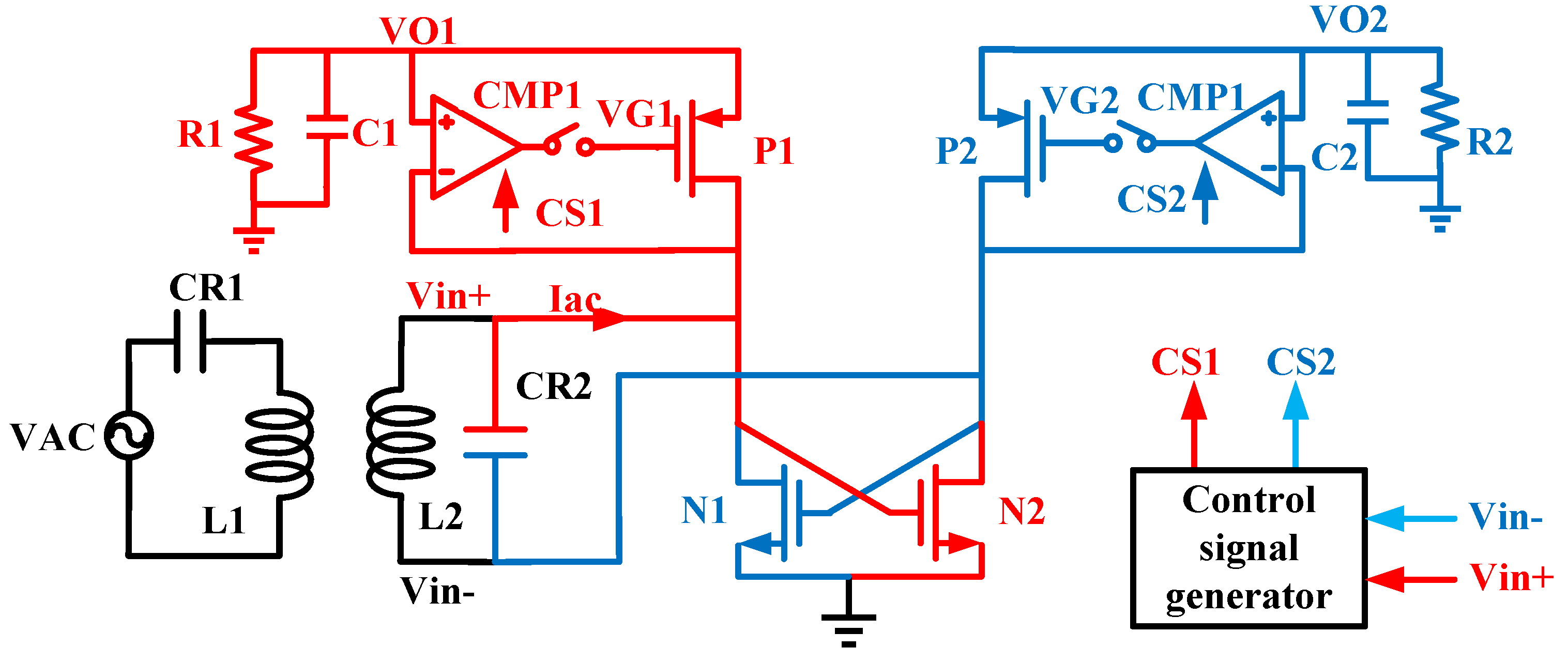
This article presents a single-stage, dual-output regulating rectifier, the diagram of which is shown in
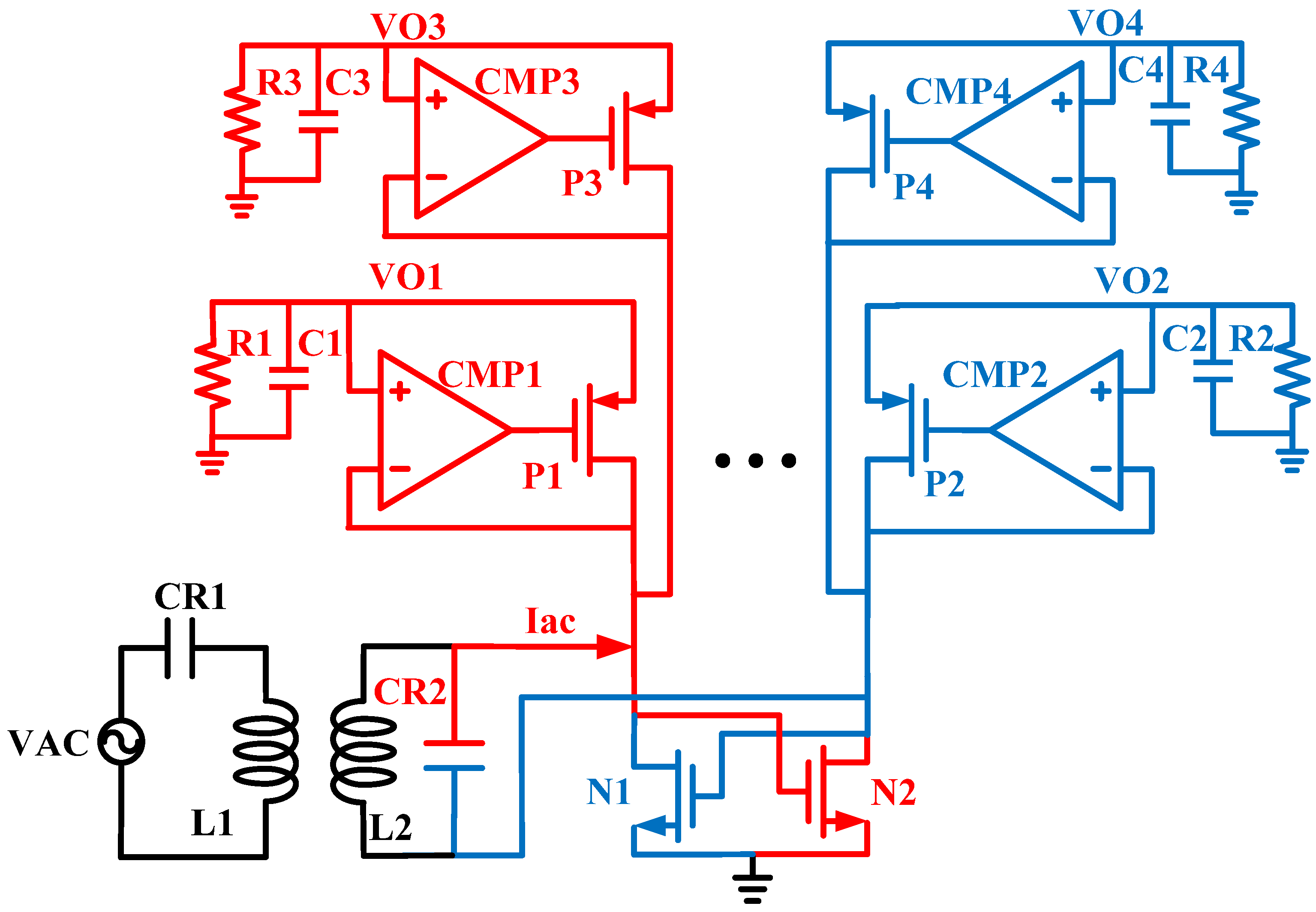
Figure 4. More outputs can be added by adding power transistors in this system, as shown in
Figure 5. Adding N more outputs necessitates N more transistors, and the transistor number of N outputs can be presented as (N + 2). The system clock doubles the input frequency and divides the input voltage into odd and even cycles.
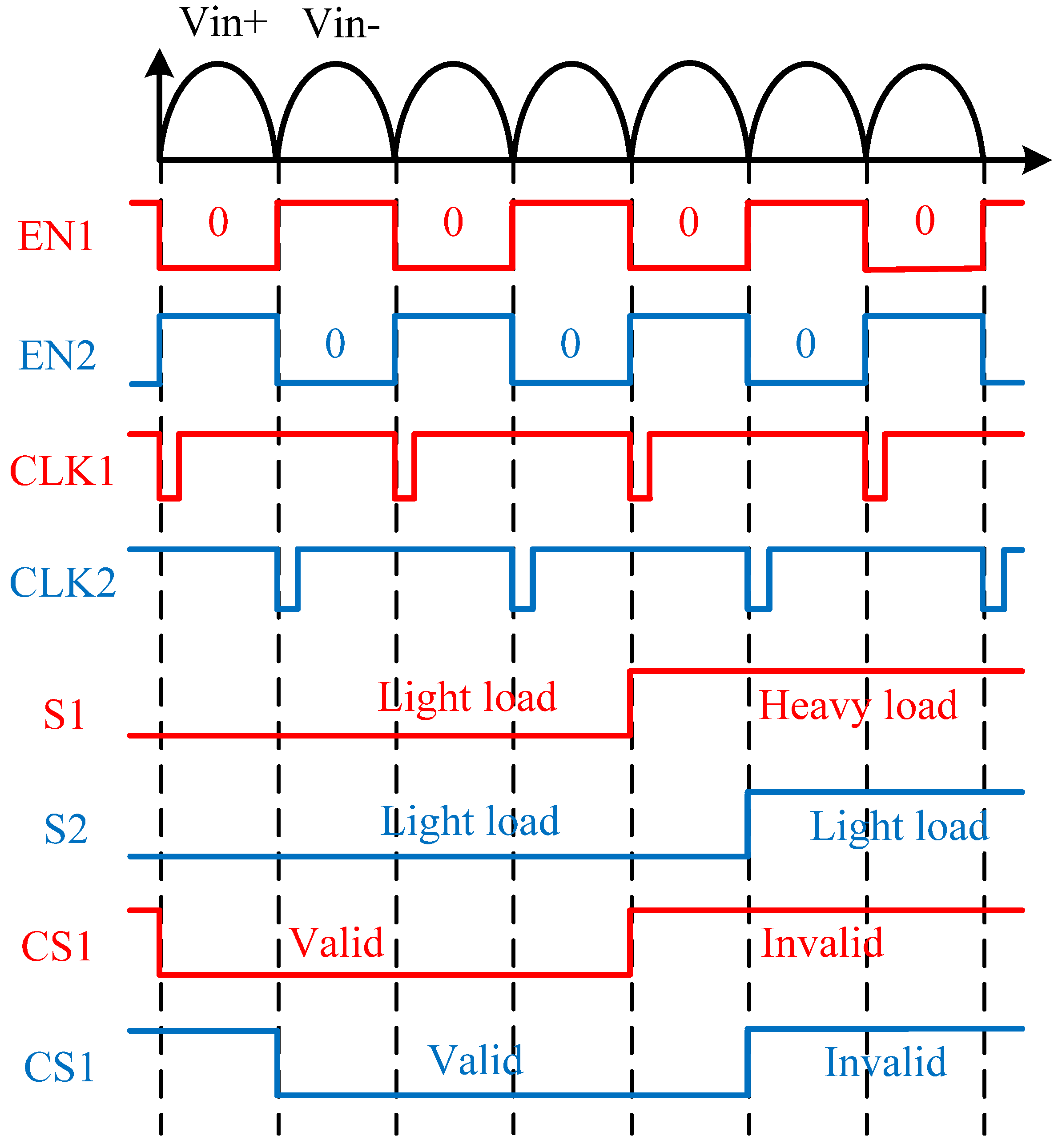
Acronyms mentioned in this paper are presented as follows: VAC is the signal source; L1 and L2 represent primary and secondary coils, respectively; CR1 and CR2 represent resonant capacitors of primary and secondary stages, respectively; Iac is the input current of the circuit; Vin+ and Vin− are the inductive voltages of secondary stages and the input voltages of the proposed circuit, respectively; comparator 1 and comparator 2 are represented by CMP1 and CMP2, respectively; VG1 and VG2 are the gate voltages of power transistors; VO1 and VO2 are dual-output voltages and are represented by VO; CS1 and CS2 represent the control signals of comparator 1 and 2, respectively; C1 and C2 are output capacitors; R1 and R2 represent output loads; Vref1 and Vref2 are reference voltages; P1, P2, N1 and N2 are power transistors.
Different output voltages occupy different phases of the input signal, which means that the output voltage VO1 only works in odd cycles, and the output voltage VO2 only works in even cycles. By comparing the output voltage VO and the input voltage Vin, the dual-output voltages are charged to the desired values.
The advantages of this system are as follows: (1) delivering two different regulating voltages in one stage simultaneously; (2) using a lower number of on-chip power transistors and other components to reduce cost; (3) eliminating cross-regulation, which occurs in the SIMO system; (4) decreasing power consumption through PSM modulation.
2.2. Working Principle
Figure 4 presents the diagram of this system. This work adopted PSM modulation to control the output voltages VO1 and VO2. The controllers sampled VO1 and VO2 and generated control signals (CS) CS1 and CS2 to control the conduction of power transistors and to determine the charging states of output voltages. The CS signals are valid at a low voltage level to charge outputs VO1/VO2 by Vin, and the CS signals are valid at a high voltage level to charge outputs VO1/VO2 by output capacitors C1 and C2. As the control signals are generated from different phases in one period of the input signal, there is only one output voltage being charged at the same time.
According to the voltage level of control signals, the system works in three different states, namely State 1, State 2 and State 3. State 1 and State 2 represent the charging mode, which means output voltages are charged by Vin in these states, and State 3 represents the discharging mode, which means output voltages are charged by the output capacitor in this state. Additionally, State 1 can be represented by CS1 = 0, CS2 = 1, VO1 < Vin+; State 2 can be represented by CS1 = 1, CS2 = 0, VO2 < Vin−; State 3 can be represented by CS1 = 1, CS2 = 1/CS1 = 0, VO1 > Vin+, CS2 = 1/ CS1 = 1, CS2 = 0, VO2 > Vin−. These are shown in
Table 1.
When the system works in State 1, power transistors P1 and N2 turn on to charge output voltage VO1, and at the same time, power transistors P2 and N1 turn off. Similarly, in State 2, transistors P2 and N1 conduct to charge output voltage VO2, while transistors P1 and N2 are cut off. In State 3, both transistors P1 and P2 shut off, and transistors N1 and N2 conduct alternately: when transistor N1 turns on, Vin+ is clamped to the ground; similarly, when transistor N2 turns on, Vin− is clamped to the ground. In this state, loads R1 and R2 are charged by output capacitors C1 and C2, respectively, which means that there is no connection between the input voltage and the output voltage.
The system adopts PSM to reduce power consumption. When VO1 > Vref1 in odd cycles and VO2 > Vref2 in even cycles, the cycles are skipped. Next, different working states are introduced according to the phases of input signals. When odd cycles arise, the output voltage VO1 and the reference voltage Vref1 are compared to determine the working mode of this system. When VO1 > Vref1, it means that the output voltage is large enough, and output voltage VO1 does not need to be charged. Then, the cycles are skipped, and the system works in discharging mode (State 3). Output voltage VO1 is powered by the output capacitor C1 in this state. However, when VO1 < Vref1, two situations can occur. If VO1 < Vin+, the power transistors P1 and N2 turn on, and the output voltage VO1 is charged by Vin+.; in this situation, the system works in charging mode (State 1). If VO1 > Vin+, the power transistors P1 and N2 turn off to cut off the channel of input and output voltages, and the output voltage VO1 is charged by the output capacitor C1; in this situation, the system works in the discharging mode (State 3).
When even cycles arise, the output voltage VO2 is compared with the reference voltage Vref2. If VO2 > Vref2, it means that the output voltage is large enough and it does not need to be charged; thus, the cycles are skipped. The system works in the discharging mode (State 3), and the output voltage VO2 is charged by the output capacitor C2. When VO2 < Vref2, two situations happen. If VO2 > Vin−, there is no current through the transistors P2 and N1, and the output voltage VO2 is charged by the output capacitor C2; in this situation, the system works in the discharging mode (State 3). If VO2 < Vin−, the transistors P2 and N1 turn on, and the output voltage VO2 is charged by Vin−. The circuit works in the charging mode (State 2). The control principle of this system is shown in
Table 1, and the control flow chart is shown in
Figure 6.
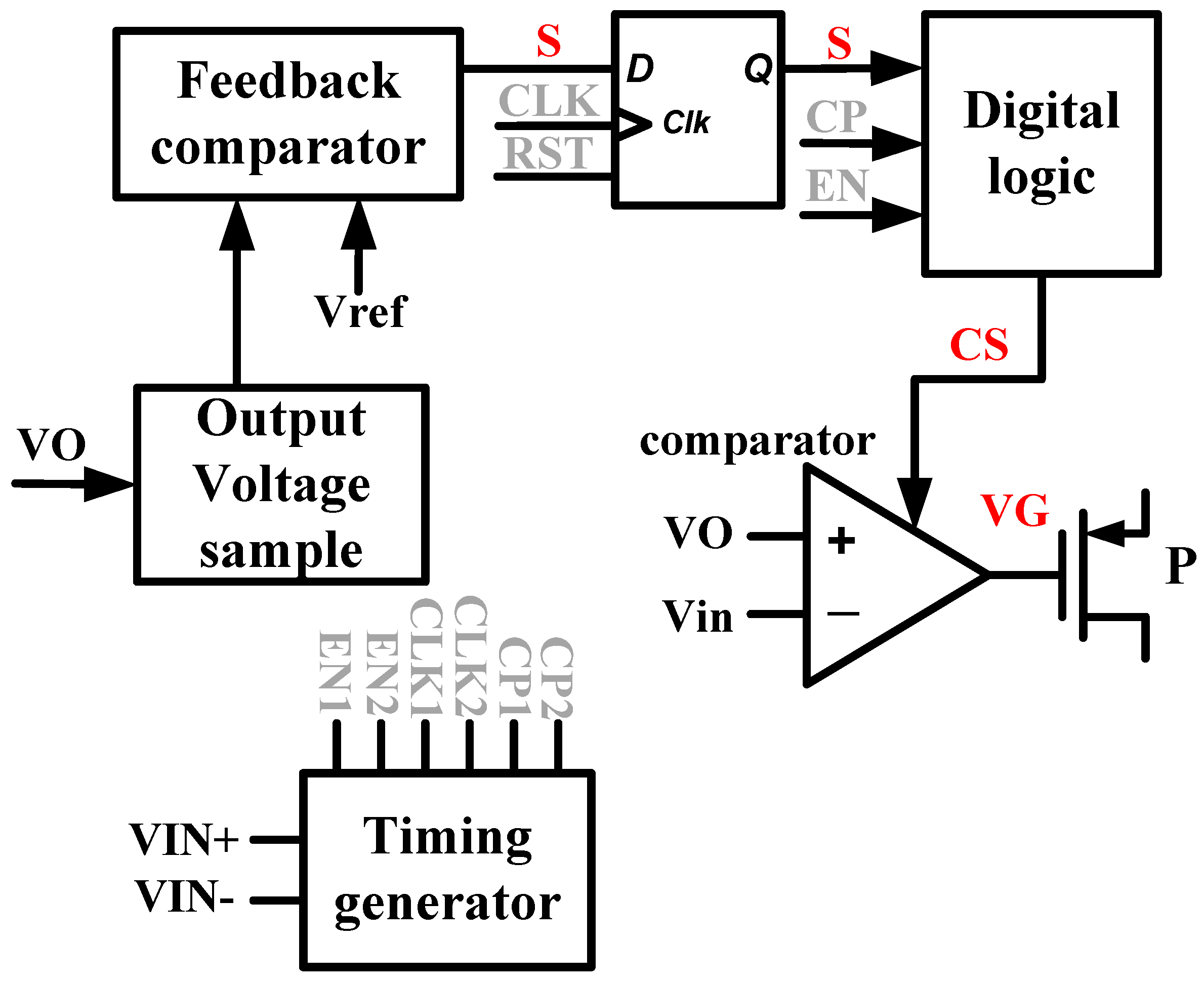
3. Implementation of the Control Signal Generator
Figure 7 presents the diagram of the control signal generator. It shows only one set of generators, and the other output has the same control structure. The timing generator produces a level signal (EN: EN1, EN2) and a clock signal (CLK: CLK1, CLK2) from Vin+ and Vin−. The clock pulse signals (CP: CP1 and CP2) defer from the CLK signals. The EN signals control the conduction of the dual-output power transistors P1 and P2 alternately, and EN = 0 is valid. The RST means a reset signal, which resets flip-flops at the start-up stage of the system, and RST = 0 is valid. The digital logic modules generate a control signal from the EN and a load signal (S) when CP signals trigger. Additionally, VO represents the output voltages VO1 and VO2.
When EN1 enables, the output voltage VO1 is sampled, and the result is sent to feedback comparator 1. Then, feedback comparator 1 generates the load signal (S1) and sends the information to flip-flop 1. When pulse signal CLK1 works, the trigger sends the load signal S to digital logic 1. Additionally, the control signal CS1 is generated and sent to comparator 1 to control the conduction state of power transistor P1, as described in
Section 2.2. Similarly, when EN2 enables, VO2 is sampled, and the result is sent to feedback comparator 2. Then, the sampling result and the reference voltage Vref are compared to generate the load signal S2 and to send S2 to flip-flop 2. S2 is delivered to the digital logic 2 module when the clock signal CLK2 arises, and the control signal CS2 is generated and sent to control the conduction state of P2 when CP2 triggers. The timing logic chart of control signals, level signals, clock signals and load signals is shown in
Figure 8.
4. Simulation Results
The single-stage dual-output wireless power receiver in this work is designed by a 0.18 μm CMOS process, and the operating frequency is 125 KHz.
Figure 9 shows the testbench of the proposed circuit. As mentioned in
Section 2, the secondary coil and the capacitor are equivalent to a voltage source due to parallel resonance, and the value of the equivalent voltage source in this circuit is Vac = ±2.5 V. R1 is a sensing resistor measuring input current Iac; Iac is represented in Equation (2) with the value of R1 as 10 Ω. The input current is necessary to calculate the power conversion efficiency, as shown in Equation (3). The system efficiency is the ratio of the output power to input power. Output power is clear: the total power of two output branches. Additionally, the input power is the average value of the production of the input voltage and the input current during some periods. Additionally, the two off-chip capacitors are 5 μF. The following simulation results are performed by using cadence.
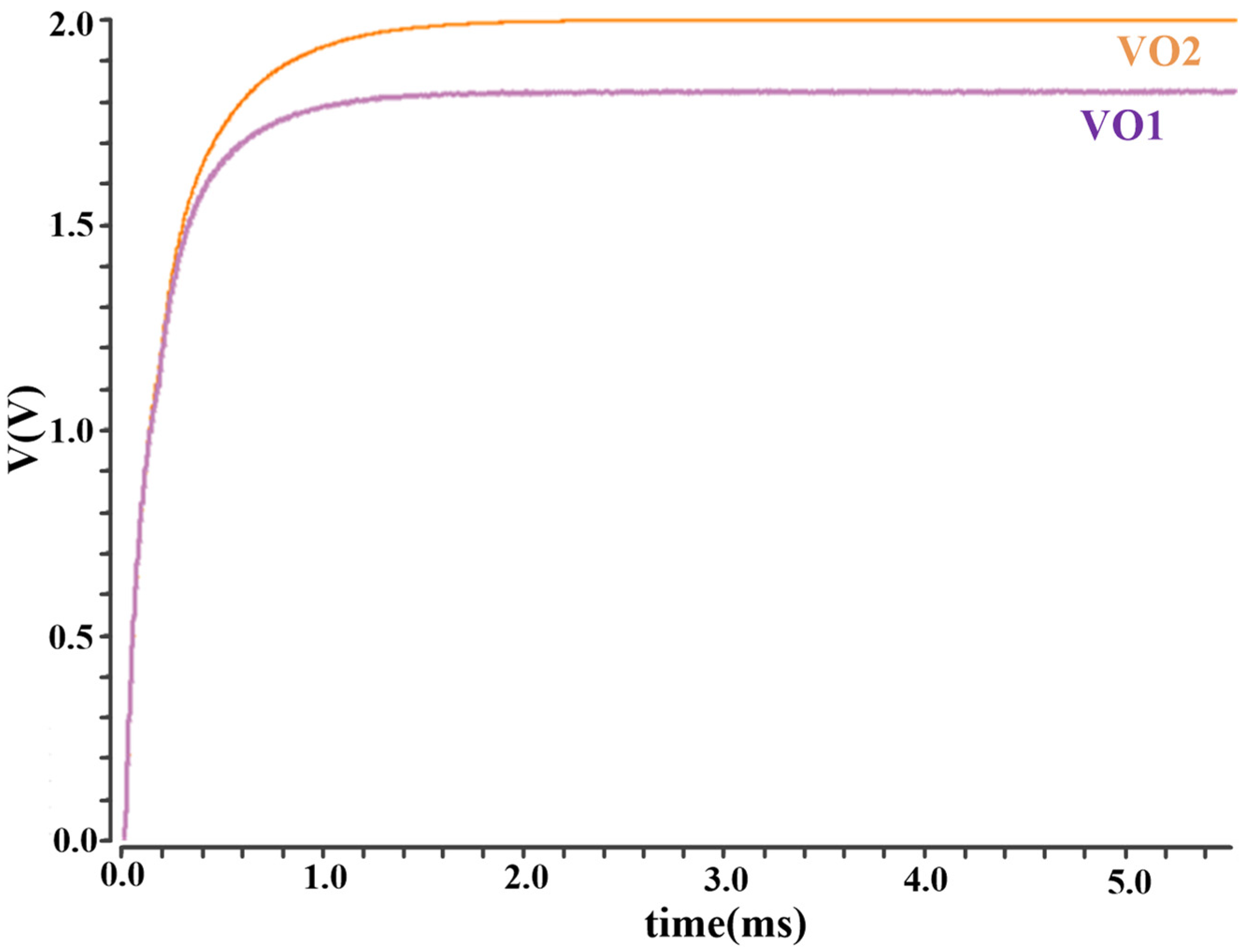
Figure 10 shows the simulation results of the dual-output voltages of this system. The dual-output voltages are 1.8 V and 2 V.
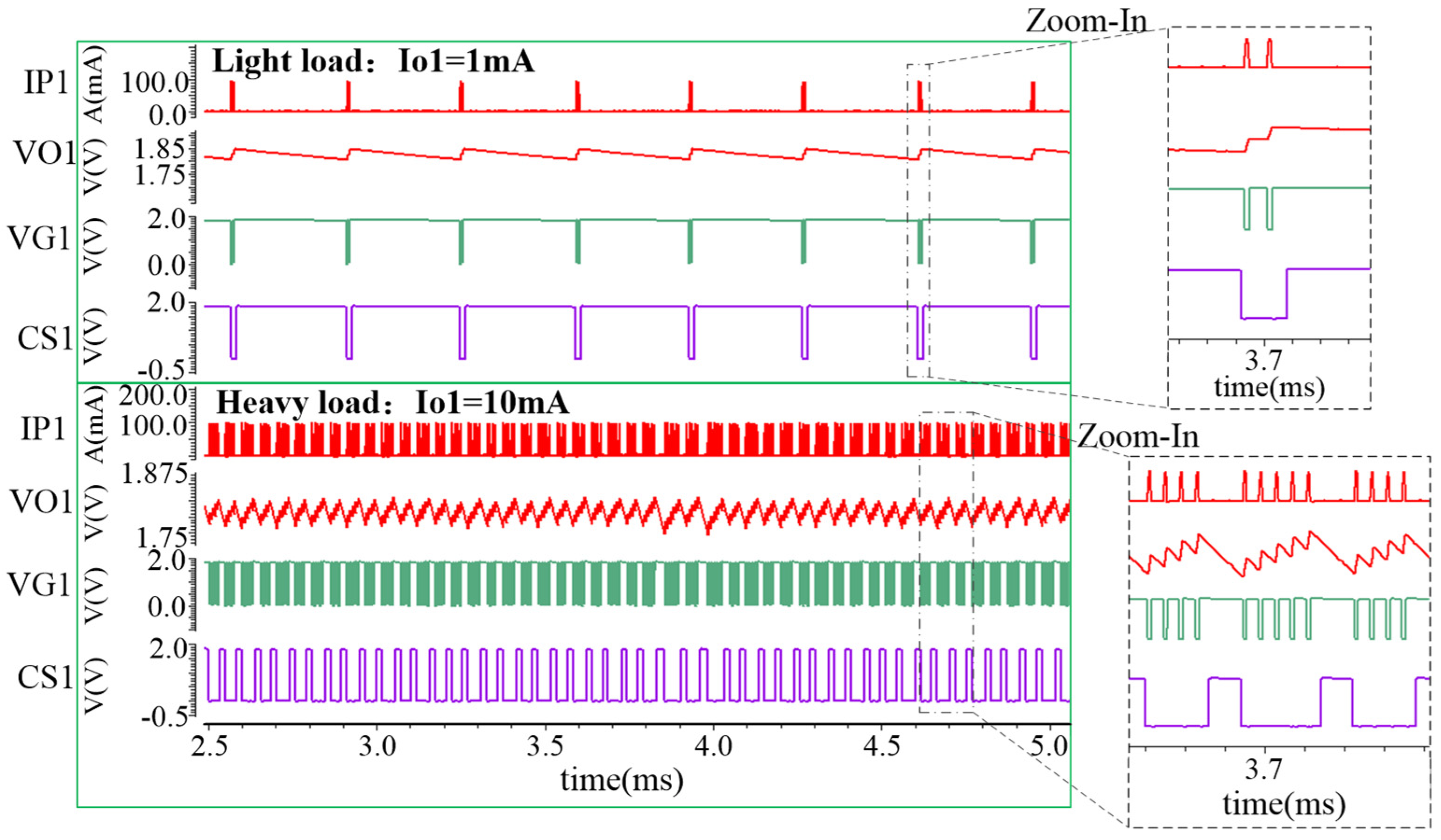
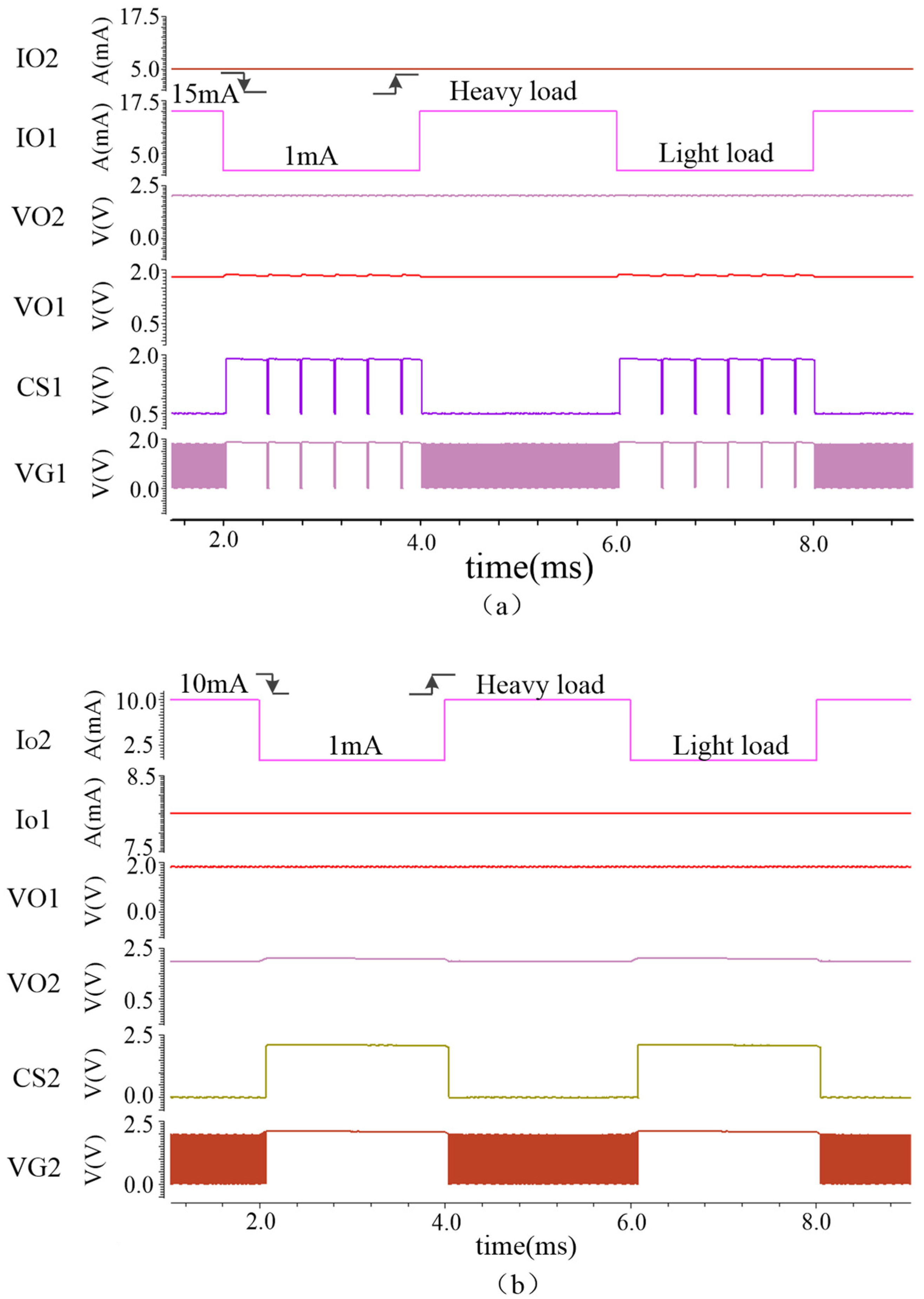
Figure 11 presents the simulation waveform when the loads are light (Io1 = 1 mA) and heavy (Io2 = 15 mA). When control signal CS1 enables, the gate voltage VG1 of power transistor P1 is able to conduct transistor P1 to charge the output voltage VO1. PSM modulation is clearly observed: the charging activity is more frequent to meet the demand of VO1 when the load is heavy, while the charging activity is less frequent, which means the system skips cycles when the load is light. Comparing the control signals of the two different loads, it is obvious that the conduction time of the control signal in a heavy load is longer than in a light load every time. Additionally, at every conduction time, the number of charging output voltages in a heavy load is more than in a light load, resulting in a denser output voltage ripple. In a light load, the transistor P1 only takes a short time to charge output voltage VO1, and during that time, the ripple of output voltage VO1 increases quickly. Then, VO1 turns into discharging time and slowly decreases; during the decreasing time, pulse skip modulation appears to skip cycles. The results of this figure are simulated where Io2 is fixed at 5 mA.
Figure 12 shows the different waveforms of the output voltage VO2 in different load situations. Similarly, every time the control signal CS2 enables, the gate voltage VG2 of the power transistor P2 is able to conduct the transistor, and the output voltage VO2 is charged. In the charging mode, the output voltage increases; on the contrary, in the discharging mode, the output voltage drops. It is obvious that the valid time of the control signal in the heavy load is longer at every conduction time, and the conduction frequency of the power transistor P2 is greater in the heavy load than in the light load. In the light load, due to the short valid time of the control signal, there are only a few charging times quickly supplying output voltage VO2 to the expected value. Then, VO2 drops slowly, and the system skips some cycles. In the heavy load, due to the long valid time of the control signal, the conduction frequency of the power transistor P2 is higher, and the charging speed is slower due to the heavy load. The results in this figure are simulated, where Io1 is fixed at 5 mA.
We can observe light loads in
Figure 11 and
Figure 12. Compared to the charging frequency of output voltage VO2, output voltage VO1 charges less and skips more cycles. VO2 charges more as the output voltage VO2 is higher. Additionally, the heavy loads of the two pictures are not comparable due to the different load currents.
To verify the cross-regulation phenomenon, transient load changes were set in the simulation environment.
Figure 13a plots the waveform of dual-output voltages VO1 and VO2, dual-output currents Io1 and Io2, the control signal CS1 and the gate voltage VG1 of transistor P1, where load R1 changes sharply from 15 mA to 1 mA and from 1 mA to 15 mA. When Io1 varies from 1 mA to 15 mA in 10 ns, it takes 15 μs to recover from the undershoot voltage of 60 mV, and we can notice that when Io1 varies, the output voltage VO1 has a undershoot voltage of 60 mV. However, output voltage VO2 has no change, which means that there is no cross-regulation when Io1 changes from 1 mA to 15 mA. Similarly, the system needs 203 μs to recover from a 60 mV overshoot voltage when Io1 changes from 15 mA to 1 mA in 10 ns, and there is no influence on the output voltage VO2, which means that there is no cross-regulation in this situation. This figure is simulated when Io2 is fixed at 5 mA.
Figure 13b plots the waveform of dual-output voltages VO1 and VO2, dual-output currents Io1 and Io2, control signal CS2 and gate voltage VG2 of power transistor P2 when the load changes between 1 mA and 10 mA. It takes 40 μs to recover from an overshoot of 60 mV when the Io2 increases from 1 mA to 10 mA in 10 ns. In this situation, the output voltage VO2 has a tiny change, and the output voltage VO1 has no variation, which means that there is no cross-regulation. Similarly, when the Io2 changes from 10 mA to 1 mA in 10 ns, the system takes 322 μs to return back from an 80 mV undershoot voltage, and there is no influence on the output voltage VO1, which indicates that there is no cross-regulation in this situation. This figure is simulated when Io1 is fixed at 5 mA.
Overall, there is no influence on one output voltage when the other output voltage changes. The reason is that the two output voltages are charged from different phases of the input signal, which eliminates the cross-regulation phenomenon that exists in the SIMO system due to the shared inductor.
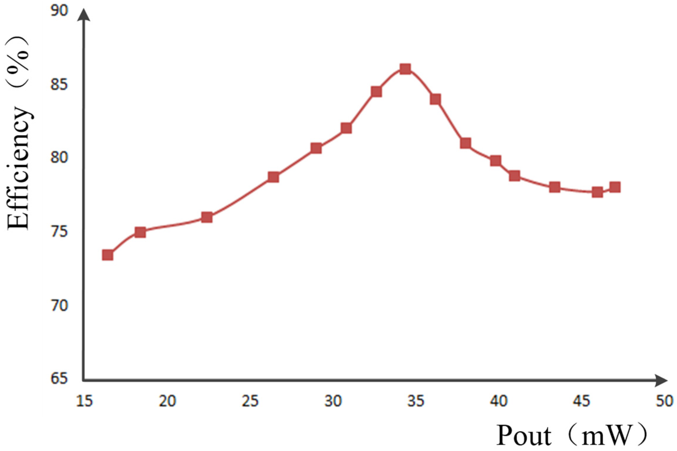
Figure 14 shows the efficiency of the proposed single-stage, dual-output receiver. A maximum efficiency of 86% can be reached in this system when the output power changes from 15 mW to 47 mW for dual-output voltages of 2 V and 1.8 V. The efficiency decreases after peak efficiency because of the increasing on-resistance losses.
Table 2 summarizes the comparison of state-of-the-art works and the proposed single-stage, dual-output wireless power receiver. ISSCC [
13] and JSSC [
5] represent two-stage AC–DC receivers with only one output voltage. TPE [
7] delivers dual-output voltages with a rectify stage and a SIMO stage. JSSC [
12] and TPE [
1] show single-stage receivers with only one output voltage. It is obvious that the efficiency of single-stage single-output receivers is higher than two-stage, single-output receivers because of the elimination of interstage loss. CICC [
15] shows single-stage, dual-output receivers with a closed-loop delay controller and ten power transistors. The work in this paper converts AC to dual-regulating DC directly in only one stage with only four power transistors. The peak efficiency of this system can reach 86% when the output power ranges from 15 mW to 47 mW due to the PSM modulation. However, this system can only realize two similar outputs, and the output power is limited.


