1. Introduction
Nowadays, more and more portable sensing systems in the form of wearable and implantable devices are being used to monitor biopotential signals from human body. Among those, the two most important are electrocardiograms (ECG) from the heart and electroencephalograms (EEG) from the brain. Electrical tissue impedance (ETI) has been used to detect the tissue composition for physiology and pathology [
1]. Local field potentials (LFPs) and action potentials (APs) are important for neuroscience research and therapy. Sensing these signals is vital for diagnosing neurological disorders, brain–machine interfaces, and neuroprosthetic technologies. Biopotential signals often have quite small amplitudes, from 10 to 100 µV for EEG and about 1 mV for ECG. These signals exist at a frequency range from 0.5 to 150 Hz [
2,
3]. The peak amplitude of LFPs and APs is about 1 mV and 100 µV, respectively. LFPs have a frequency band from 0.5 to 200 Hz, while that of APs runs from 300 Hz to 10 kHz [
4].
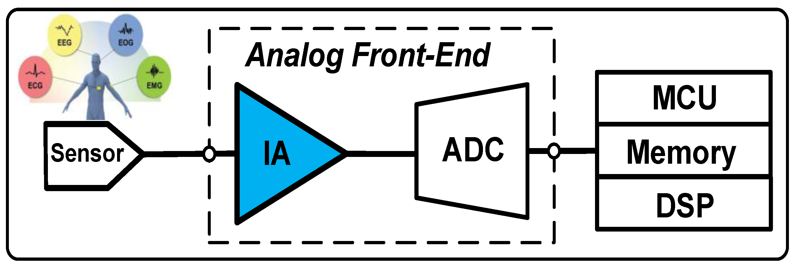
To read out the inherently low-power biopotential signals, the acquisition system, illustrated in
Figure 1, often consists of an instrumentation amplifier (IA). This amplifier is known for its high input impedance and operation at a low frequency of biosignals. However, at this frequency range, flicker noise is the dominant noise source. To suppress this noise, switched-biasing and bulk-switching techniques, also called as chopping techniques, have been previously investigated in [
5,
6]. However, these techniques cause output ripples as the upmodulated offset is added by an integrator stage. Several approaches have been proposed to reduce these ripples. Passive ripple reduction approaches were introduced by different authors in [
7,
8]. In [
7], a large chip area low-pass filter (LPF) is added at the output stage to filter out the output ripple. The cutoff frequency of the LPF must be much lower than the chopping frequency that affects the bandwidth of the amplifier [
9]. In [
8], a high-power efficiency DC blocking is inserted at the output of the input stage to prevent the current offset through the output chopper and the integrator output stage. However, these amplifiers all suffer from the noise aliasing issue due to the added capacitor inside the chopper loop [
10].
Active approaches were proposed by [
9,
11,
12] to mitigate the drawbacks of the passive approaches. In [
9], a combination of passive and active approaches was proposed. This technique uses a larger capacitor at the output of the first stage; therefore, the amplifier still suffers from noise aliasing issue as per [
8]. In [
11], a switched-capacitor notch filter is added to the input of the output stage to filter out the signals causing output ripple. However due to the phase delay, this architecture suffers from instability around chopping frequency
fCH [
13]. In [
12], a ripple reduction loop (RRL) using the auto-zero approach has been investigated. This technique allows the instrumentation amplifier to achieve a low output ripple. However, this approach utilizes an AC-coupled capacitor to sense output ripple, which increases the output load [
13].
In this paper, a low-power and low-noise CCIA with a higher ripple attenuation factor (RAF) is presented. The proposed architecture employs a modified RRL with a low-pass filter that is equivalent to an auto-zero offset cancellation loop (A-OCL) to remove the inherent intrinsic offset due to process variation. The G
m1’s output offset is sensed and reduced by adjusting the transconductance gain through the A-OCL. In addition, to achieve a highly efficient silicon chip area, a T-network capacitor [
14] is also introduced to play the role of the negative feedback capacitor. The rest of this paper is organized as follows:
Section 2 introduces the structure of the proposed capacitive-coupled chopper instrumentation amplifier (CCIA), applying a new chopping technique based on the zero offset cancellation loop.
Section 3 details the circuit implementation of the feedback loop, including the operational amplifier (op amp) block and its feedback loop.
Section 4 discusses the simulation results and benchmarking with recent research results.
Section 5 concludes the paper.
2. Design
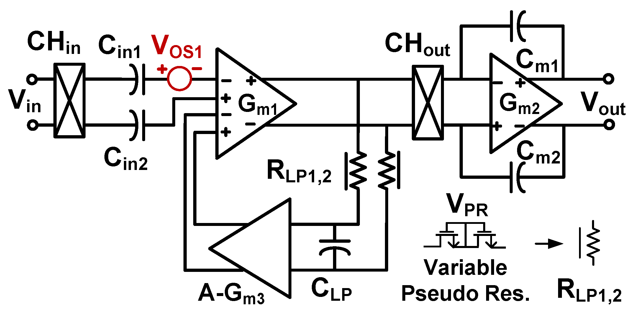
Figure 2 illustrates the schematic of the proposed CCIA [
15], which consists of two transconductor stages. The first stage employs folded-cascode amplifier topology (G
m1), while the second adopts a single common source amplifier (G
m2) for higher output swing. An auto-zero offset cancellation loop (A-OCL) is applied for the first G
m1 stage. A T-cap loop (TCL) is introduced to the second G
m2 stage and fed back to the input of the first stage. Due to unavoidable process variation during fabrication, the G
m1 is attached with an intrinsic offset V
os1 that creates an output ripple considered as noise and affects the output signal. Therefore, an A-OCL with a new chopping technique is inserted to the CCIA to reduce the output ripple while assuring that loading effect is not added to the amplifier. This technique can remove flicker noise so that low-noise amplifier can be achieved.
The common-mode voltage VCM is set to 0.5 V for Gm1 through two pseudoresistors Rp1,2. The neural input signal Vin is upmodulated to the chopping frequency band by the chopper CHin, then downmodulated to the baseband by CHout. The chopping frequency fCH is fixed at 10 kHz. To set the DC gain of CCIA to 100 dB, the quiescent currents Gm1 and Gm2 are selected as 980 nA and 180 nA, respectively. The closed-loop gain of the CCIA of 40 dB is defined by the ratio of the input capacitor Cin1,2 and the feedback capacitor Cfb1.2.
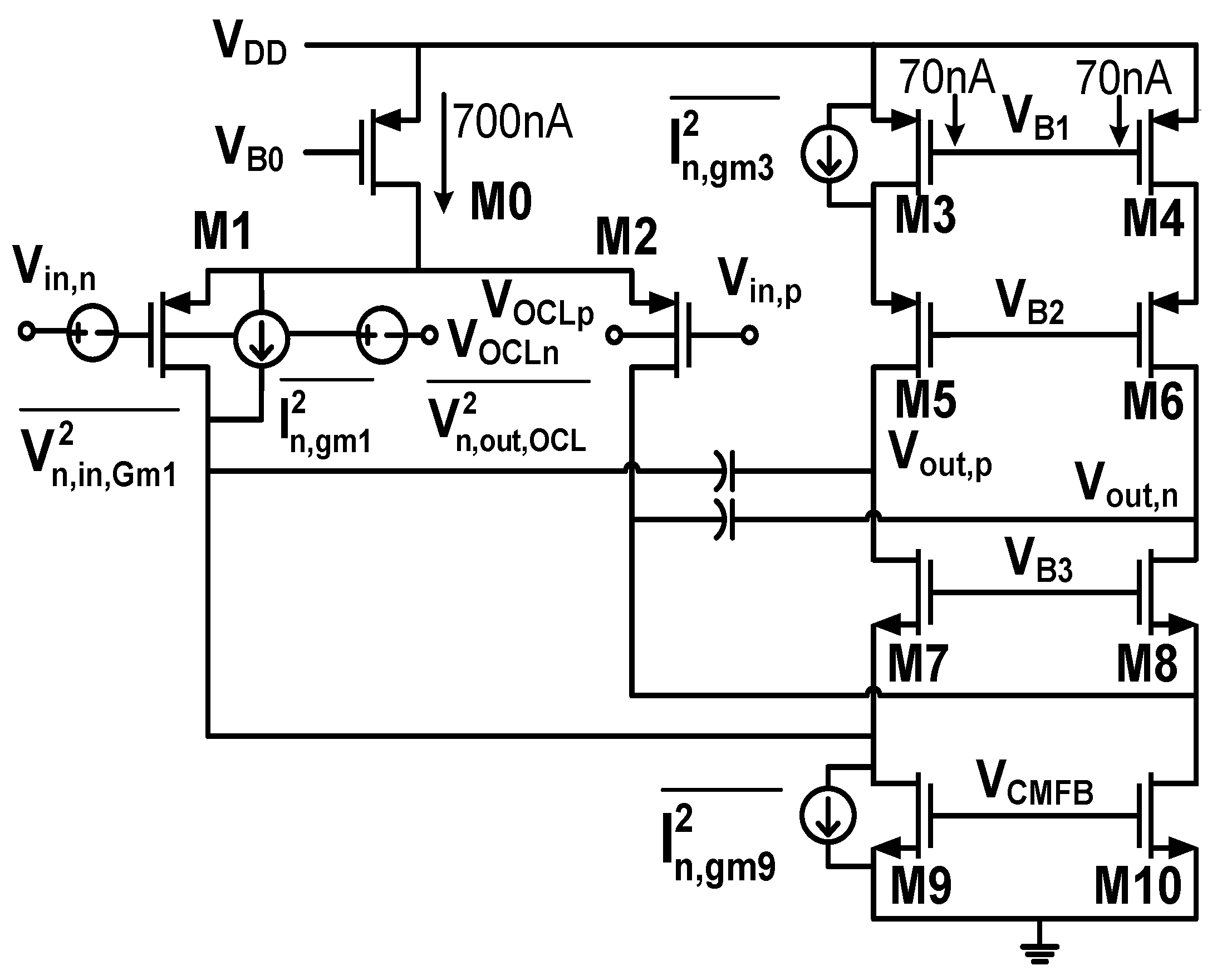
Figure 3 shows the schematic of the main path of CCIA with proposed A-OCL in feedback loop with the G
m1. This feedback loop consists of an active RC low-pass filter employing an NMOS pseudoresistor, a capacitor, and a A-G
m3 that contains the transconductor G
m3 and will be detailed in the next paragraph. In a conventional A-OCL approach, as in [
4], the cancelation of output offsets
VOS1, caused by the transconductor G
m1, is realized by adding two transconductors G
m3 and G
m4 to create a negative offset compensation. The residual input signal V
in,ω and the intrinsic offset V
OS1 of the transconductor G
m1 result in the two respective currents at its output. They are I
1,ω at the chopping frequency band and the offset current I
1,OS at the signal base-band. To suppress V
1,OS, the third transcoductor G
m3, to form an integrator, and the fourth transconductor G
m4 are integrated to generate a negative output offset voltage to add to the output offset voltage V
1,OS to compensate for each other. This conventional A-OCL is also called a negative A-OCL. The main drawback of this approach is its complex design and high-power consumption. In our design, the G
m4 is not needed; the transconductor G
m3 is connected to a new scheme in a feedback loop to cancel the offset voltage of the G
m1. The A-OCL is connected from the output of the G
m1 to its input voltage instead of from the output of the G
m2 to the output of G
m1 as in the conventional approach. In the proposed approach, the compensation occurs at the input of G
m1 so all the variations associated with mismatches due to PVT (process, voltage, and temperature) are also canceled. The cancellation analysis is detailed as follows.
When chopping is applied for the amplifier, the finite bandwidth of the amplifier creates the output ripple V
OUT,Ripple at the chopping frequency
fCH [
12], which can be expressed as follows:
where C
m1,2 is the Miller compensation capacitor. By the feedback operation, V
OUT, Ripple is reduced by a factor of the DC loop gain L
G(0) [
9]. For the proposed A-OCL, L
G(0) can be written as
where A
3 is the finite DC gain of the transconductor G
m3 in A-OCL. The η = G
mb1/G
m1 is around 0.25 [
16].
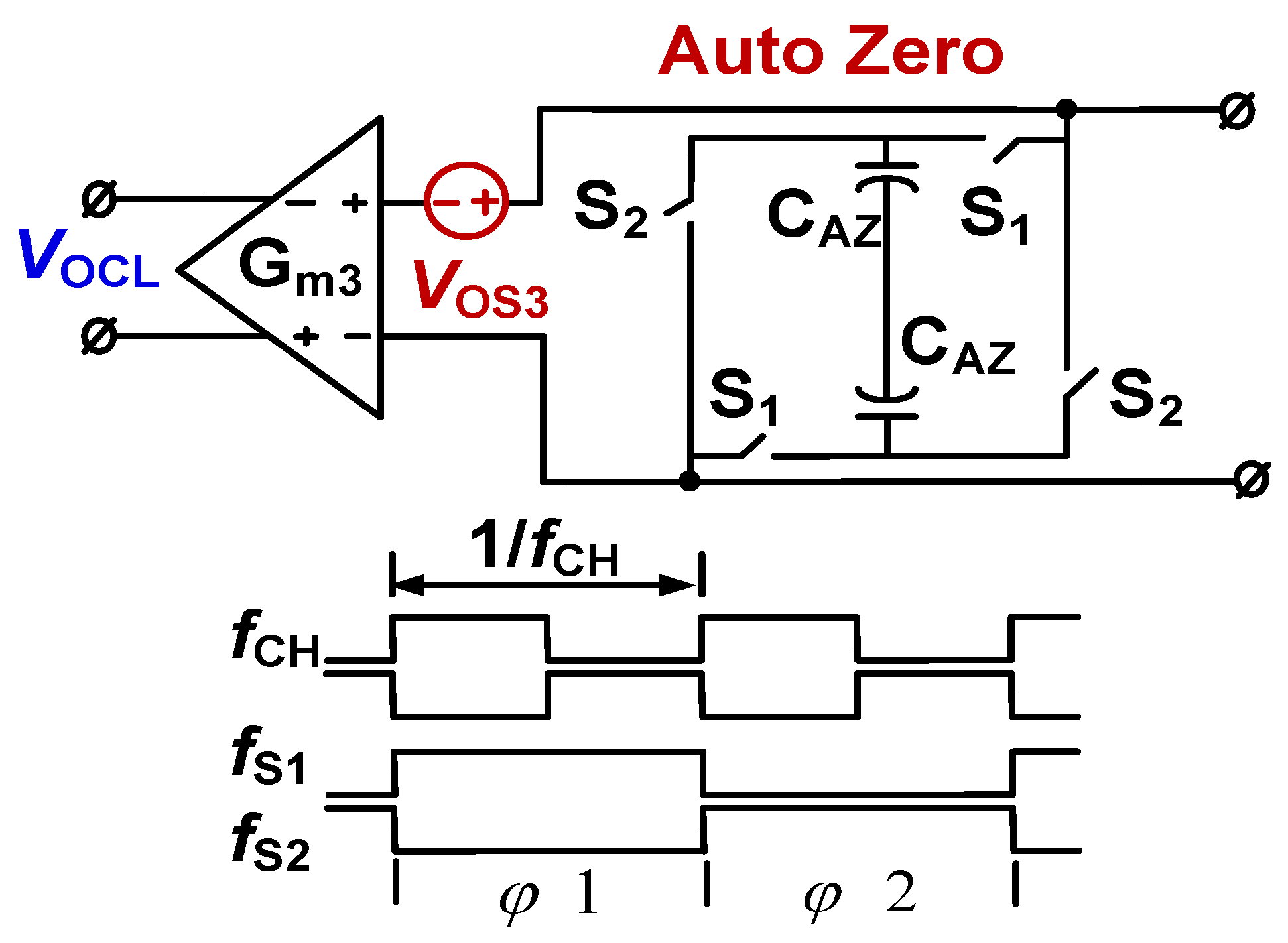
Figure 4 shows the schematic of A-G
m3, including the proposed auto-zero (AZ) offset technique, by controlling the switches S
1,2, the transconductor G
m3, and the timing diagram. Because of the process variation, G
m3 is also associated with an intrinsic offset V
OS3, which contributes to the output ripple as well. Therefore, the auto-zero (AZ) technique is applied to reduce the offset voltage V
OS3. The operation of switches S
1,2 is controlled by the control signals
fS1,2, as shown in the timing diagram of
Figure 4, which are chosen at 50% of chopping frequency
fCH. The auto-zero loop, independent of
fCH, does not affect the operated rippled reduction. During φ1, the V
OS3 is charged to the stored capacitor C
AZ. During φ2, the charged voltage in the capacitor C
AZ is charged to the opposite input of G
m3. Hence, the DC voltage at the differential input of G
m3 is balanced so that the offset voltage of G
m3 can be suppressed.
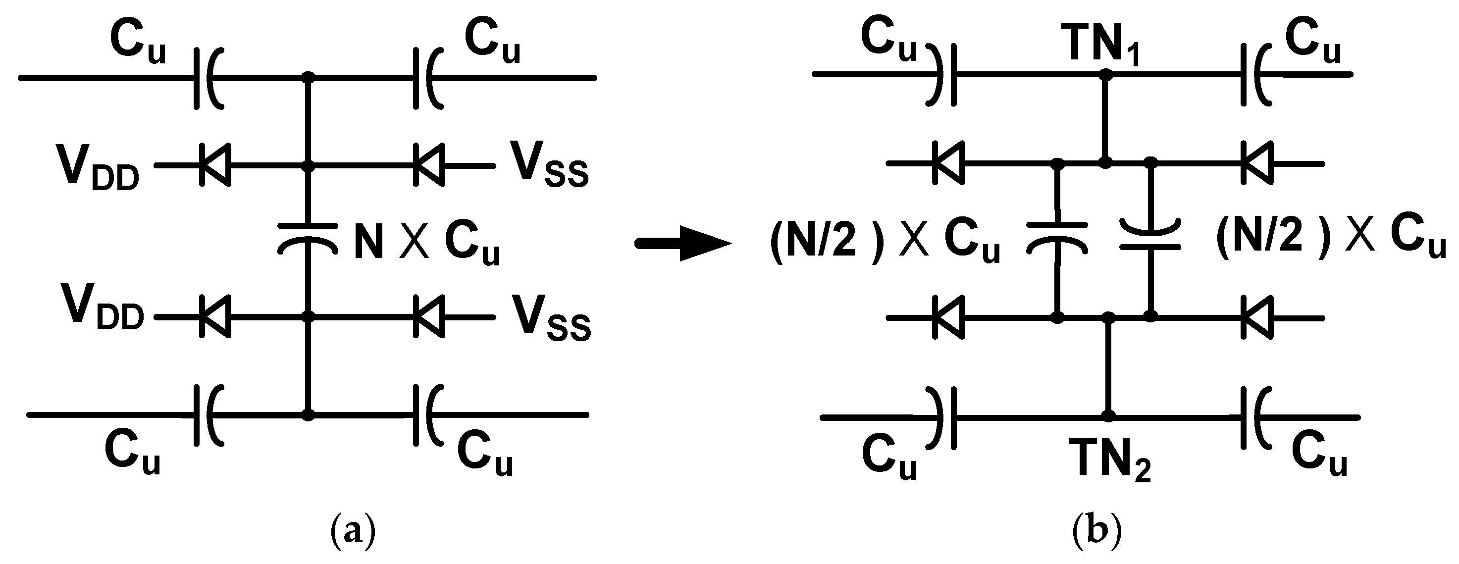
In the CCIA, the mid-band gain is defined by C
in1,2/C
fb,eq. Increasing C
in1,2 for a higher gain results in reduction of the input impedance Z
in as well as an increase in the chip area. The minimum capacitance C
fb,eq that can be designed is limited by the technology. To reduce the chip area without increasing the input capacitor C
in1,2, a T- network capacitor [
14] is employed. Considering differential operations, C
fb,eq, realized using the T-network capacitor, can be expressed as follows:
where
N is the number of unit capacitors C
U = 200 fF used to implement the shunt capacitor
N × C
U (see
Figure 4). The T-network capacitor in the feedback path, as illustrated in
Figure 5, increases the closed loop gain by shunting some of the feedback signals. As a result, C
fb,eq is reduced for a given gain. It is noticed that the overall area saving is achieved by the decrease in the C
in1,2 value enabled by the T-network capacitor. Increasing
N can further reduce C
fb,eq and the chip area, resulting in increased noise [
14]. Considering this tradeoff, the value of
N is set to 4. This approach allows us to reduce the area of C
in1,2 and C
fb,eq by 45.6%. A gain of 40 dB was achieved by using C
in1,2 of only 2 pF. In previous works, the values of C
in1,2 are much higher, such as 12 pF [
12], 10 pF [
17], and 21 pF [
18].
The T-network capacitor will increase the asymmetry between the nodes connected to the feedback network. To tackle this drawback, the configuration of the T-network capacitor is modified. N × CU is divided into two (N/2) × CU pieces, connected symmetrically to balance the parasitic behavior at two nodes TN1 and TN2. Then the top side of CU is connected to reduce the parasitic capacitance.
3. Circuit Implementation
Figure 6 and
Table 1 show the folded cascode op amp for G
m1 using the body control technique and the dimension of the MOSFETs adopted in the schematic of the op amp, respectively. All the transistors are set to work in the subthreshold region for the sake of power efficiency. To isolate the body-control terminals from the noise coupled through the substrate, a deep n-well is used for the input differential pair. The bias current of G
m1 is 840 nA. The CMFB circuit (not shown) generates the output V
CMFB2 using a 140 nA bias current.
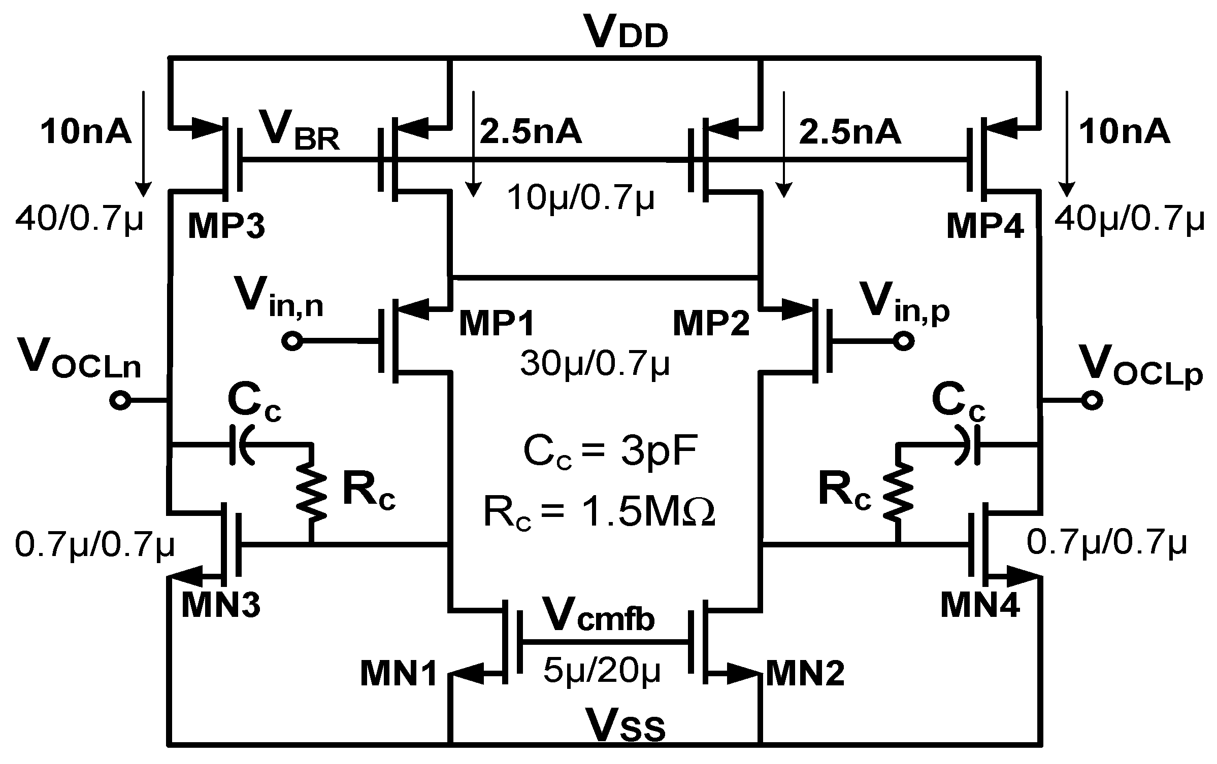
Figure 7 shows a schematic of the two-stage op amp for G
m3. In order to achieve high output swing, the output stage of G
m3 utilizes a class-A amplifier. The biased current for G
m3 is shown in
Figure 7.
Using the noise equivalent circuit shown in
Figure 6, the input referred noise of G
m1,
, can be expressed as follows:
where
is the output referred noise of the A-OCL and
n = 1.5 is the subthreshold slope factor [
17]. As mentioned above, the flicker noise of A-OCL is also modulated by the chopper technique at the output of G
m1, so the contribution of noise from A-OCL can be negligible. It is also confirmed by simulation results that the output noise of A-OCL is about
10
−15 V
rms. So the input referred noise of the CCIA can be calculated as follows:
where C
tot = C
in1,2 + C
fb1,2 + C
p, C
p is the parasitic capacitance,
are the input-referred noise of G
m1, and g
mi represents the transconductance of the transistors in G
m1.
4. Simulation Results
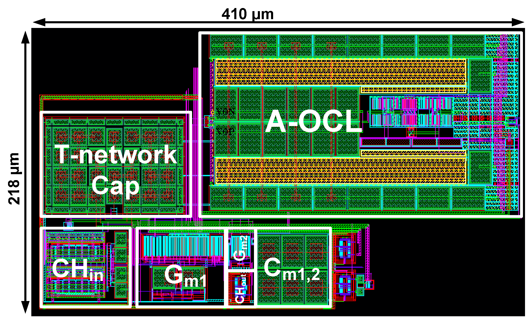
Figure 8 shows the CCIA layout using 180-nm CMOS technology, in which the core occupies an area of 0.09 mm
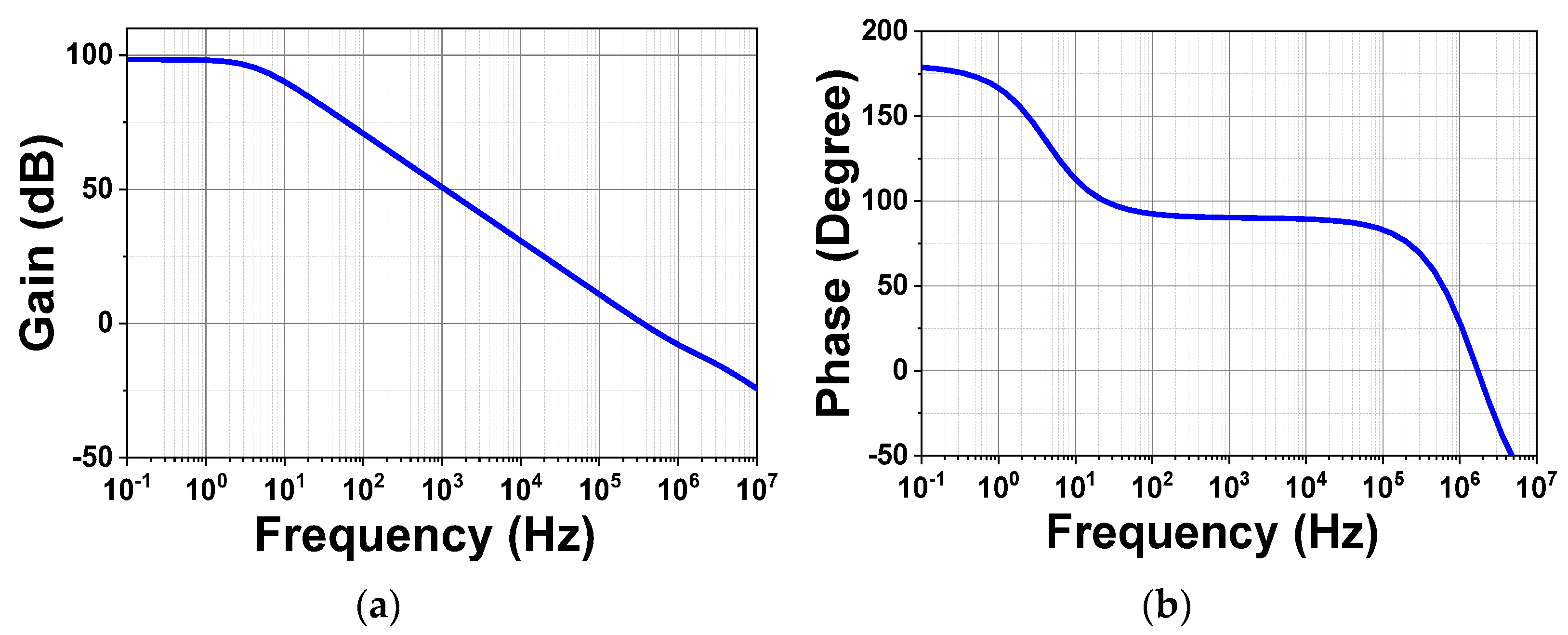
2. From this section onward, all post-simulation results, in a standard 0.18-µm CMOS technology, are carried out with a full extraction of parasite by choosing RCC option. Open-loop simulations are run to observe the gain bandwidth and the phase margin of the main path amplifier with active A-OCL. As shown in
Figure 9, the gain bandwidth is achieved at 300 kHz, corresponding to a phase margin of about 60 degrees. The frequency response of the CCIA in a closed loop is presented in
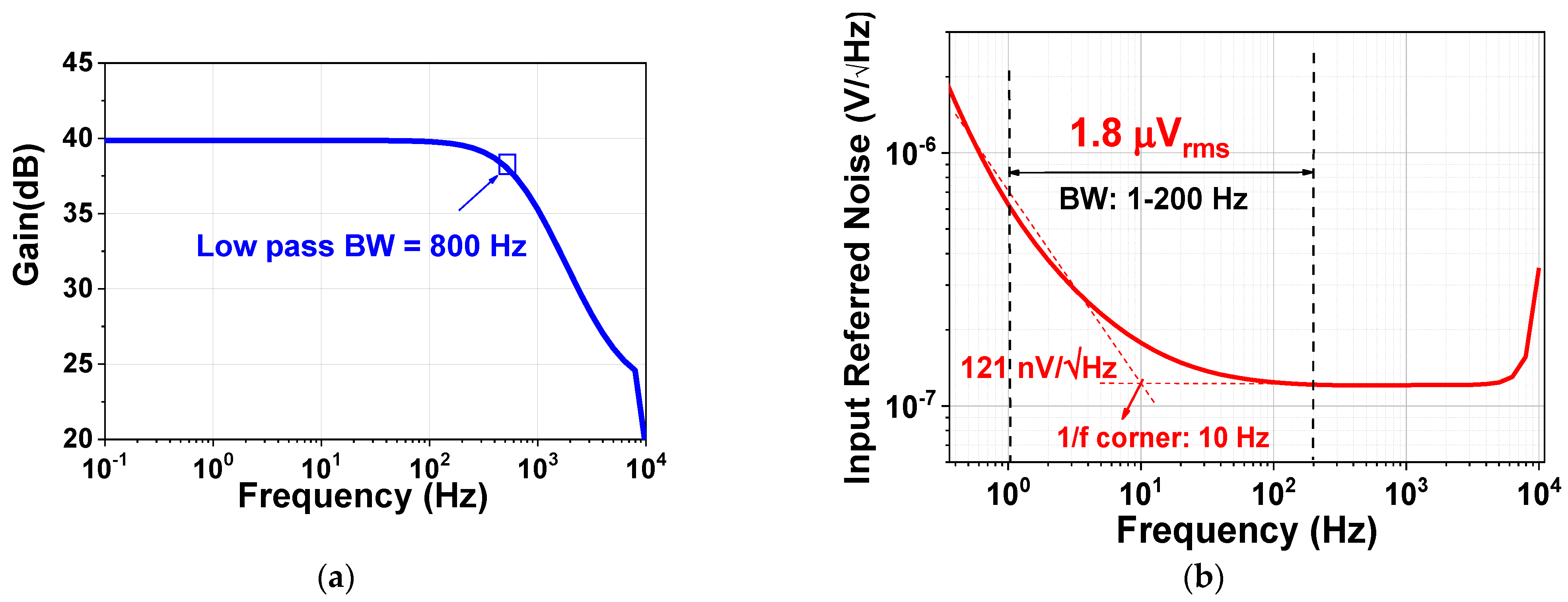
Figure 10. A closed-loop gain of 40 dB is observed with a low-pass cutoff frequency at 800 Hz (
Figure 10a). In addition, the integrated input referred noise (IRN) reaches 1.8 µV
rms over a bandwidth of 200 Hz at a thermal noise of 121 nV/√Hz and a 1/f corner of 10 Hz (
Figure 10b).
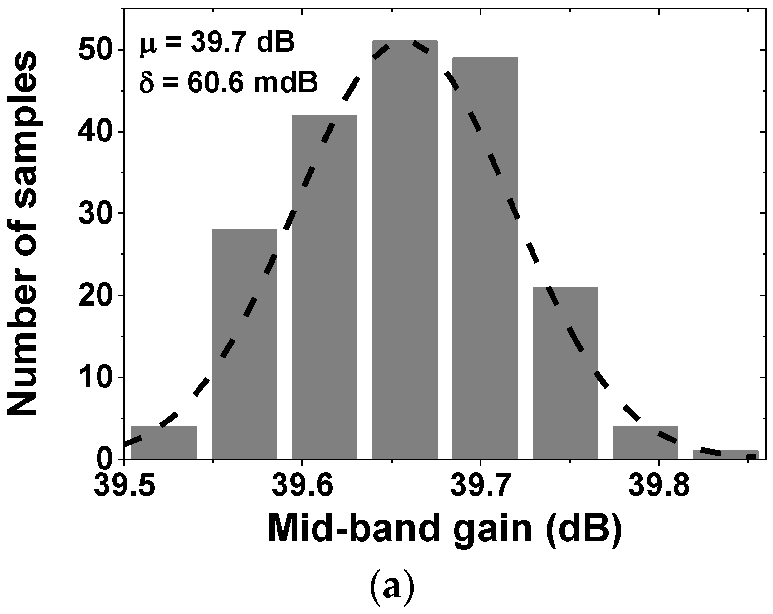
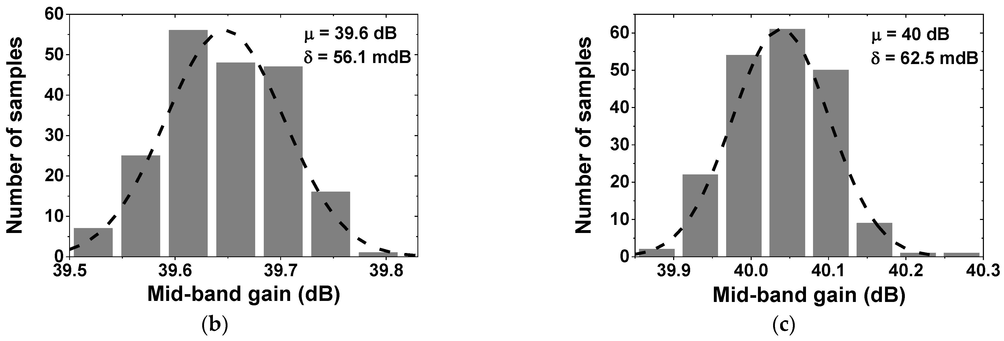
In order to verify the impact of variations in the fabrication process and power supply on the proposed CCIA, a Monte Carlo simulation was carried out by considering the local and global mismatches due to the process corner.
Figure 11 shows the Monte Carlo simulation results of the mid-band gain of the CCIA obtained using 200 samples. At V
DD = 1 V, as shown in
Figure 11a, the average mid-band gain is 39.7 dB, with a standard deviation of 60.6 mdB. V
DD varies by about 10% and the mid-band gain changes from 39.6 to 40 dB with corresponding standard deviations of 56.1 and 62.5 mdB, respectively.
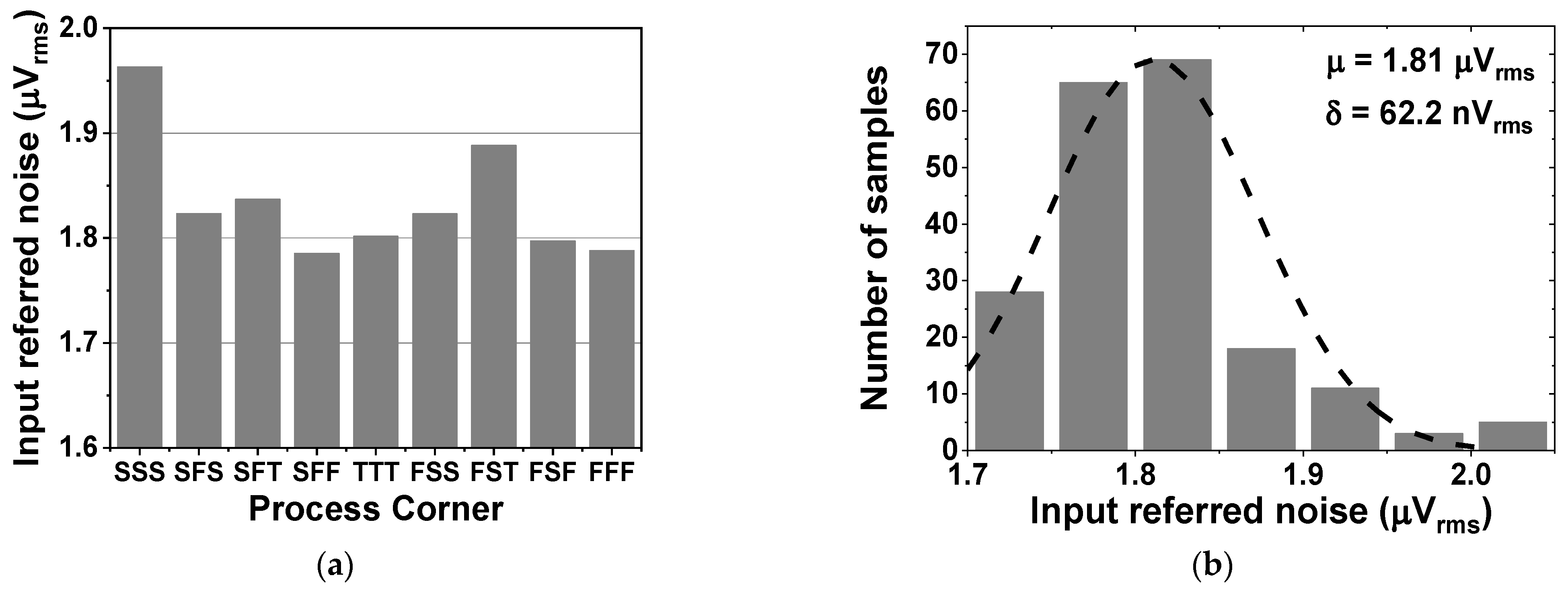
Monte Carlo simulations, with random device mismatches to investigate the effect of process corners on the noise, were realized.
Figure 12a shows that the input-referred noise of the proposed amplifier varied from 1.78 µV
rms to 1.96 µV
rms across different process corners.
Figure 12b shows that the average input-referred noise was 1.81 µV
rms, with a standard deviation of 62.2 nV
rms.
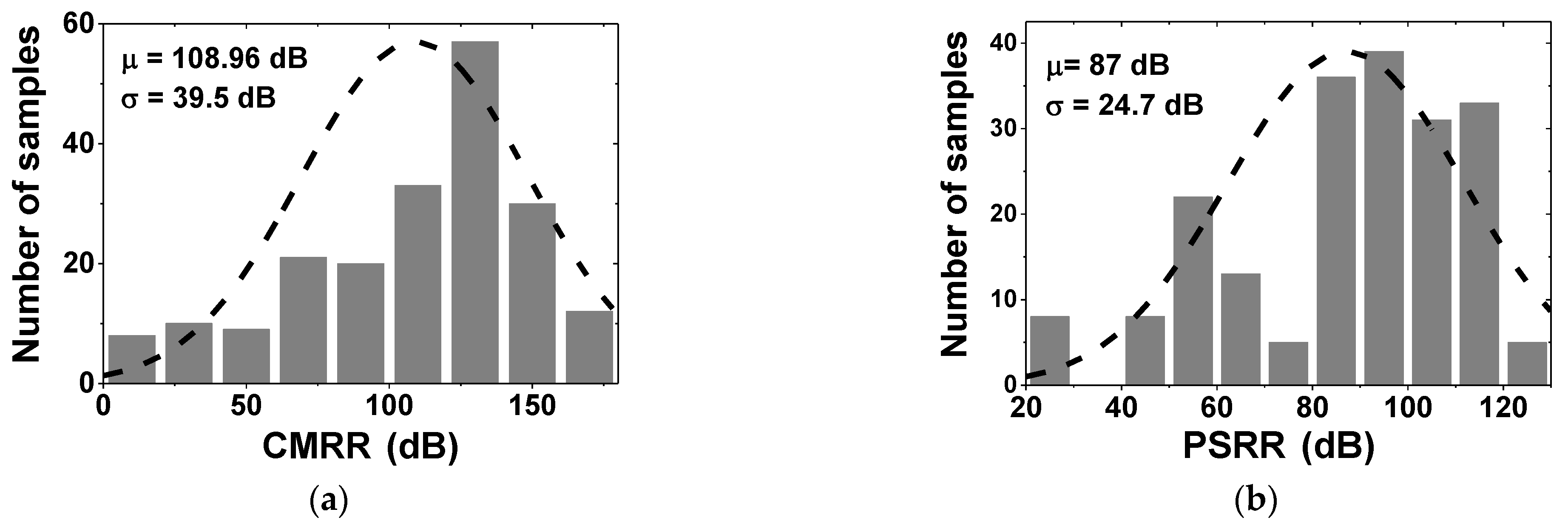
Figure 13 shows the Monte Carlo simulation results of the proposed CCIA, referring to the common mode rejection ratio (CMRR) and power supply rejection ratio (PSRR). By running 200 samples, the CCIA achieved a mean value of CMRR of 108.9 dB and PSRR of 87 dB with standard deviations of 39.5 and 24.7 dB, respectively. The CCIA’s input was set to be short-circuited during the simulation to measure the output spectrum. Both VOS1 and VOS3 were set to 5 mV.
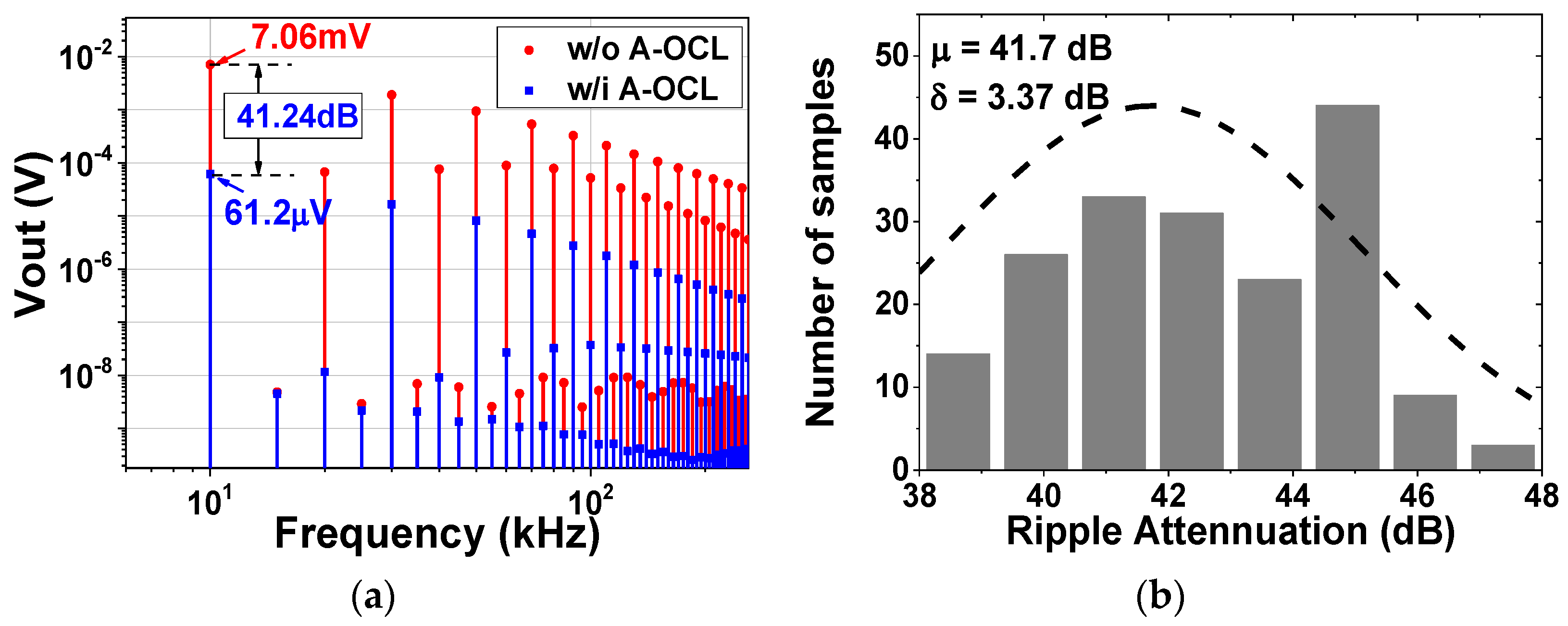
Figure 14 illustrates the output spectrum voltage and Monte Carlo simulation of the ripple attenuation factor (RAF). When A-OCL was disabled, the output spectrum at chopping frequency was around 7 mV. This spike in the CCIA was reduced to 61 µV when A-OCL was enabled, which allowed RAF to achieve a high value of 41 dB. The RAF was also double-checked by running 200 samples in the Monte Carlo simulation, considering local and global process variations, which obtained a mean value of RAF of 41.7 dB with a standard deviation of 3.37 dB. A significant reduction in the output ripple voltage was observed, which confirmed that the mismatches due to the PVT-generated offset voltage (VOS1, VOS3) can be compensated for by the proposed feedback loop.
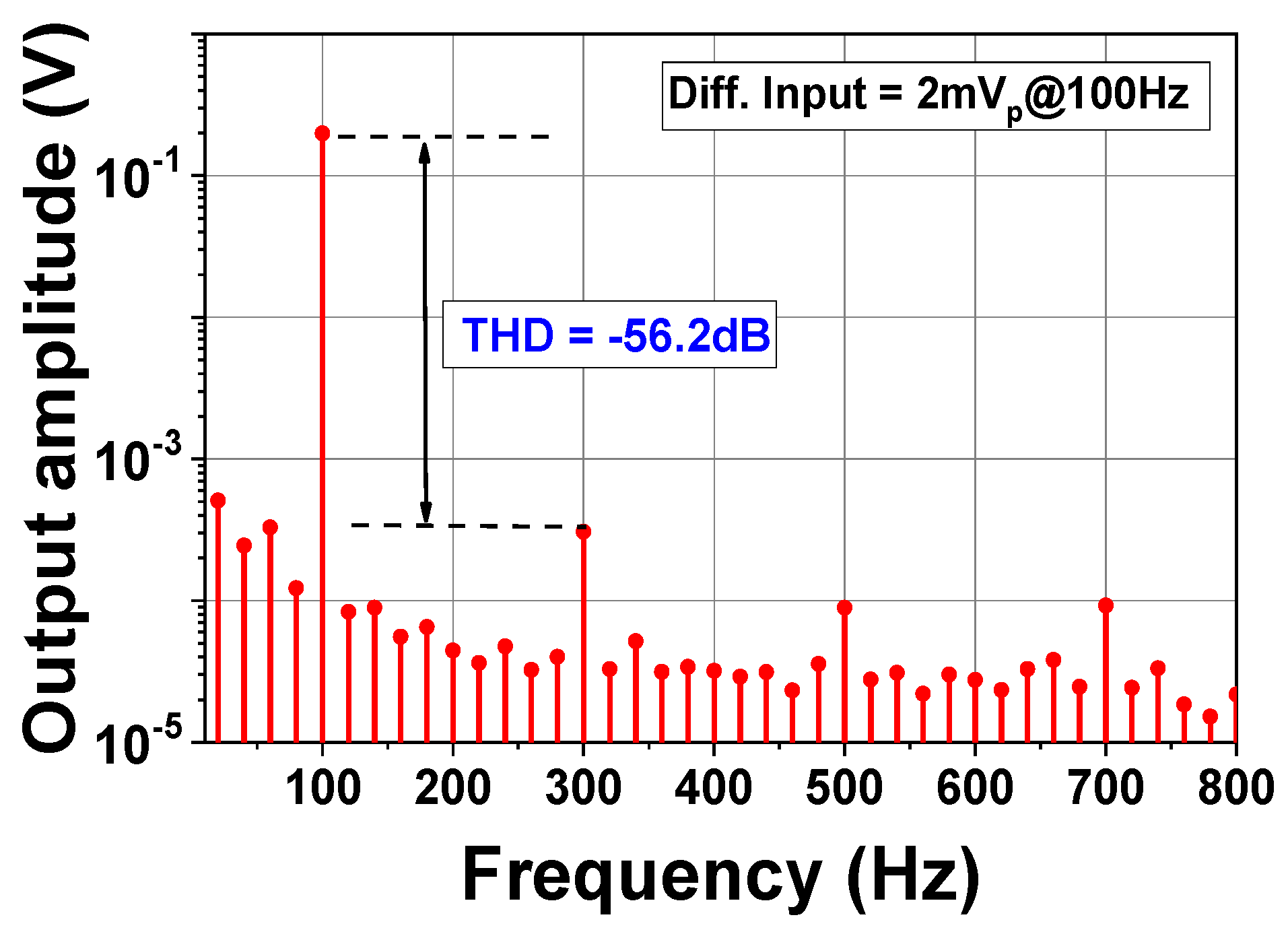
To verify the linearity of the amplifier, an FFT of output voltage is analyzed with a differential input of 2 mV and an input frequency of 100 Hz (
Figure 15). The total harmonic distortion was about −56.2 dB, which is determined by the ratio between the output amplitude at the input frequency and its third-order harmonic of 300 Hz, given that the fifth- and seventh-order harmonics are small enough to be ignored.
The power breakdown of the proposed CCIA is given in
Table 2. The power efficiency factor (PEF) is used to evaluate the tradeoff between noise and power efficiency for biopotential amplifiers. As in [
18], PEF is calculated as follows:
where V
ni,rms is the input-referred noise voltage, P
DC is the power consumption, and BW is the amplifier bandwidth. The performance of the proposed design, in comparison with state-of-art studies, is shown in
Table 3.


