This section is organized as follows.
Section 2.1 gives a brief introduction to our previous COM ASIP ISA (i.e., COM ASIP ISA V2).
Section 2.2 describes the details of a highly secure hashing algorithm, named GCM [
13,
14]. This algorithm is used by COM ASIP V3.
Section 2.3 describes details of a new concept, named two-layer security, that is used by our ASIP to increase the security of the original GCM [
13,
14].
Section 2.4 describes the changes needed in our ASIP components to support the hashing instructions.
Section 2.5 describes the additions that we made in the ISA of our ASIP to support these hashing instructions.
2.1. A Brief Introduction to COM ASIP ISA V2
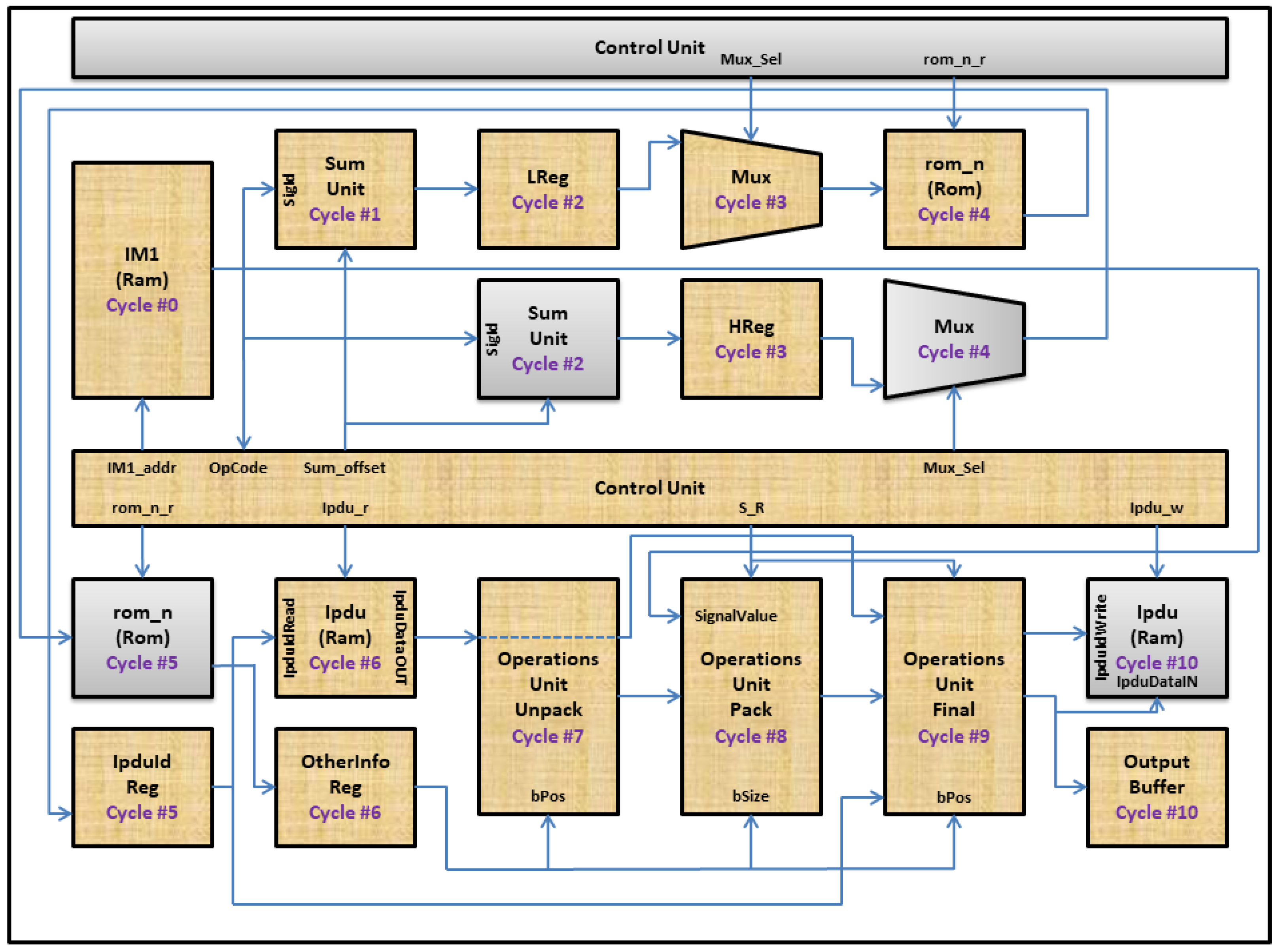
Our previous ISA consists of four phases. These phases are fetching, decoding, execution, and delivery. The execution phase consists of two sub phases (i.e., extraction and packing/unpacking). Our previous ISA supports four instructions (i.e., send signal, receive signal, send long signal, and receive long signal). Each instruction requires 12 cycles (i.e., cycle 0 to cycle 11) to complete its execution.
2.1.1. Actions in Cycle 0
The instruction memory component, named IM1, is activated by the control unit component to fetch a new instruction. The address of this instruction is specified by the IM1_addr control signal.
2.1.2. Actions in Cycle 1
The control unit component decodes an instruction fetched in the previous cycle (i.e., cycle 0) to get three pieces of information, as shown in
Figure 3. The first piece, named OpCode, is an instruction type that defines whether this instruction is a send signal, a receive signal, a send long signal, or a receive long signal instruction. The second piece, named SigId/Virtual Signal Id, is an identifier for a virtual signal that is currently processed by this instruction. The third piece, named SigValue/Virtual Signal Value, is a new value for a virtual signal that is currently processed by this instruction.
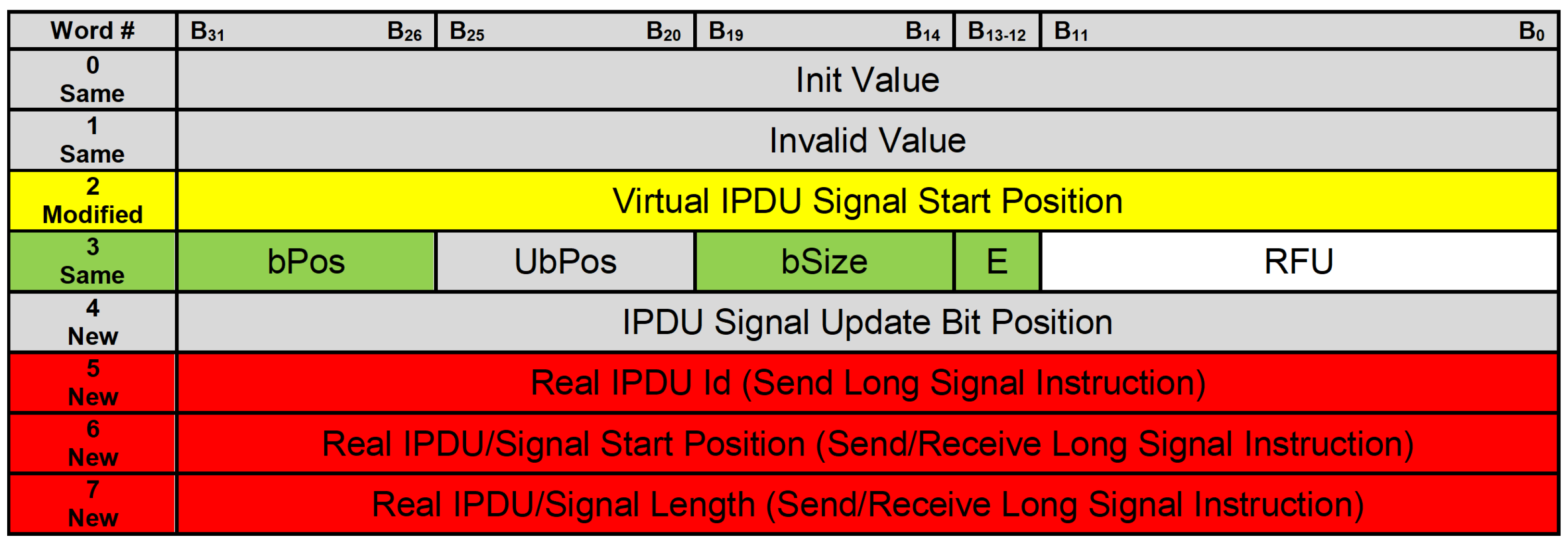
For each virtual signal, there are eight words related to this virtual signal that are saved in a read only memory (ROM) component, named rom_n. These words contain properties that represent which PDUs contain these virtual signals and how these virtual signals are placed inside their corresponding PDUs. The structure of the rom_n component is shown in
Figure 4.
Send Signal and Receive Signal Instructions
We are interested in two words, which are the third and the fourth words. The third word contains the virtual IPDU signal start position that represents the start position of an 8-byte window inside the PDU. This 8-byte window contains a currently processed virtual signal. The fourth word contains four properties that represent how a virtual signal is placed inside its corresponding 8-byte window inside the PDU. These properties are bPos (corresponds to ComBitPosition in the context of AUTOSAR Com [
8]), UbPos (corresponds to ComUpdateBitPosition in the context of AUTOSAR Com [
8]), bSize (corresponds to ComBitSize in the context of AUTOSAR Com [
8]), and E (i.e., Endianness).
Send Long Signal and Receive Long Signal Instructions
We are interested in three additional words, which are the sixth, seventh, and eighth words. The sixth word contains the real IPDU Id, which represents an identifier for a PDU that contains a currently processed virtual signal and its corresponding real signal as well. The seventh word contains either real IPDU start position or real signal start position. Real IPDU start position will be used in a send long signal instruction to give a position, inside the IPDU component, to lower SW layers to access PDUs after adding (i.e., packing) new values for virtual signals to them. Real signal start position will be used in a receive long signal instruction to give the application layer a position, inside the IPDU component, to access real signals that correspond to virtual signals that are being processed by currently executed instructions. The eighth word contains either real IPDU length or real signal length. Real IPDU length will be used in a send long signal instruction along with real IPDU start position to transfer data, as some of PDUs transmitted from the IPDU component to lower SW layers. Real signal length along with real signal start position will be used in a receive long signal instruction to transfer data from the IPDU component to the application layer.
In cycle 1, the control unit component multiplies SigId by 8 and adds a constant value (i.e., 2) to it to get address of the third word related to this virtual signal in the rom_n component.
2.1.3. Actions in Cycle 2
The control unit component multiplies SigId by 8 and adds a constant value (i.e., 3) to it to get address of the fourth word related to this virtual signal in the rom_n component.
In addition, the control unit component saves the processed SigId (i.e., (SigId * 8) + 2) from the previous cycle (i.e., cycle 1) in the low address register component, named LReg.
2.1.4. Actions in Cycle 3
The control unit component saves the processed SigId (i.e., (SigId * 8) + 3) from the previous cycle (i.e., cycle 2) in the high address register component named HReg.
The control unit component also activates a multiplexer, named Mux, to make its output come from the LReg component.
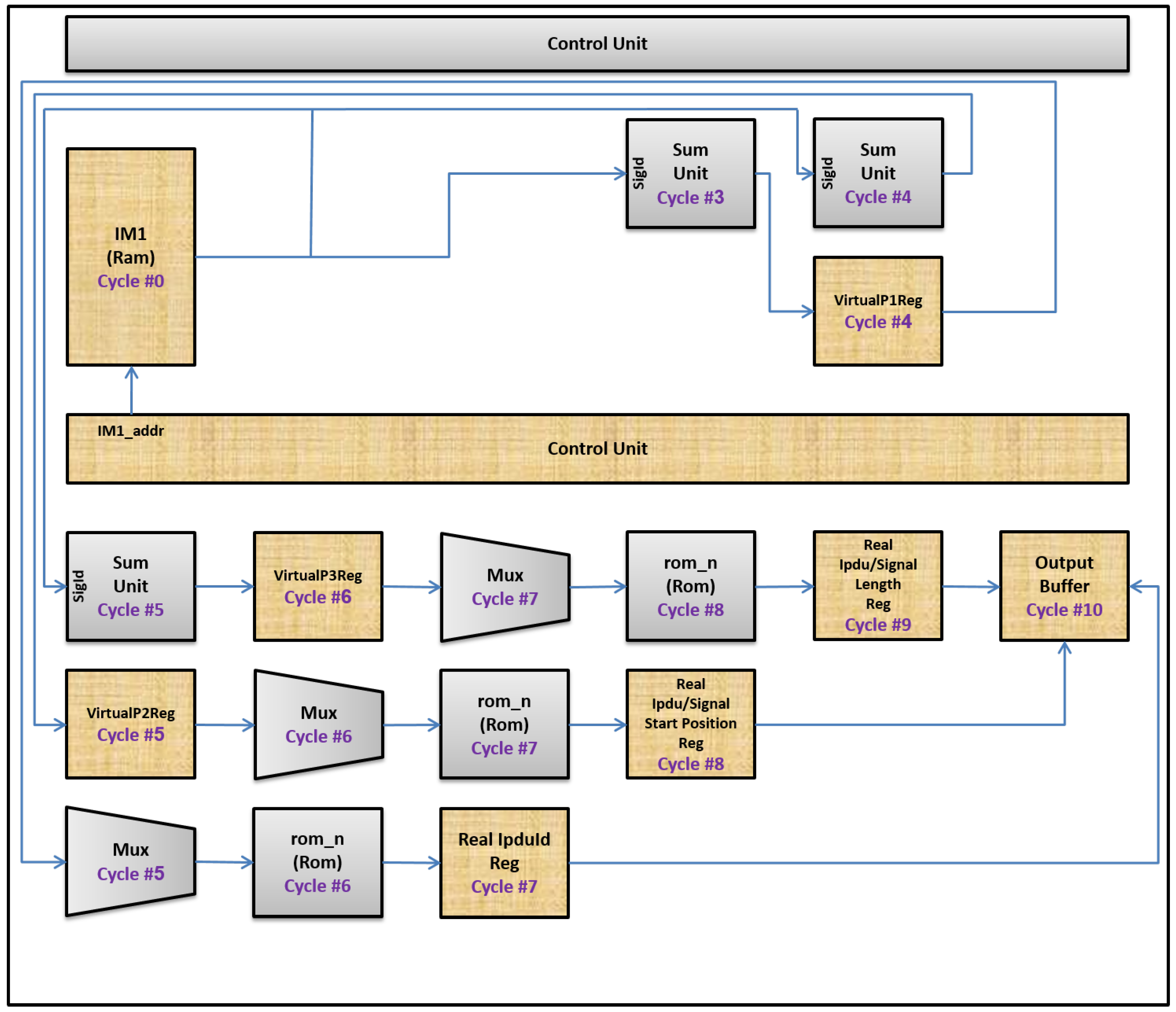
Only for Send Long Signal and Receive Long Signal Instructions
The control unit component multiplies SigId by 8 and adds a constant value (i.e., 5) to it to get address of the sixth word that corresponds to this virtual signal in the rom_n component.
2.1.5. Actions in Cycle 4
The control unit component activates the rom_n component to read a word from it. The address of this word comes from the LReg component. Data inside the rom_n component at this address contain a virtual IPDU signal start position for a PDU that corresponds to a currently processed virtual signal.
The control unit component also activates the Mux component to make its output come from the HReg component.
Only for Send Long Signal and Receive Long Signal Instructions
The processed SigId (i.e., (SigId * 8) + 5) from the previous cycle (i.e., cycle 3) is saved in the VirtualP1Reg register. In addition, the control unit component multiplies SigId by 8 and adds a constant value (i.e., 6) to it to get the address of the seventh word that corresponds to this virtual signal in the rom_n component.
2.1.6. Actions in Cycle 5
The virtual IPDU signal start position is saved in the IPDU Id Reg component.
The control unit component also activates the rom_n component to read another word from it. The address of this word comes from the HReg component. Data inside the rom_n component at this address contain those four properties that we mentioned above (i.e., bPos, UbPos, bSize, and E). Those properties represent how a virtual signal is placed inside its corresponding 8-byte window inside PDU.
Only for Send Long Signal and Receive Long Signal Instructions
The processed SigId (i.e., (SigId * 8) + 6) from the previous cycle (i.e., cycle 4) is saved in the VirtualP2Reg register. In addition, the control unit component multiplies SigId by 8 and adds a constant value (i.e., 7) to it to get the address of the eighth word that corresponds to this virtual signal in the rom_n component. In addition, the control unit component activates the Mux component to make its output come from the VirtualP1Reg register.
2.1.7. Actions in Cycle 6
The word that is read from the rom_n component in the previous cycle (i.e., cycle 5) is saved in the OtherInfo Reg component.
The control unit component also activates the IPDU component. The IPDU component contains current runtime values for PDUs, to read the current runtime value for an 8-byte window inside the PDU, named the original IPDU value, which corresponds to a currently processed virtual signal. The address used to access the IPDU component comes from the IPDU Id Reg component.
Only for Send Long Signal and Receive Long Signal Instructions
The processed SigId (i.e., (SigId * 8) + 7) from the previous cycle (i.e., cycle 5) is saved in the VirtualP3Reg register. In addition, the control unit component activates the Mux component to make its output come from the VirtualP3Reg register. It also reads a word from the rom_n component; the address of this word comes from the VirtualP1Reg register. This word represents Real IPDU Id. It will be saved in the real IPDU Id Reg component in the next cycle (i.e., cycle 7).
2.1.8. Actions in Cycle 7
The operations unit unpack component uses two inputs, which are bPos, of a currently processed virtual signal, and the original IPDU value. These inputs are used to extract a 32-bit shadow, named original shadow. In case of a send signal/send long signal instruction, this original shadow will be used to place a new value for this currently processed virtual signal in its corresponding 8-byte window inside PDU. In case of a receive signal/ receive long signal instruction, this original shadow will be used to extract current runtime value for this currently processed virtual signal from its corresponding 8-byte window inside PDU.
Only for Send Long Signal and Receive Long Signal Instructions
The control unit component activates the Mux component to make its output come from the VirtualP3Reg register. It also reads a word from the rom_n component, and address of this word comes from the VirtualP2Reg register. This word represents either the real IPDU start position, in case of a send long signal instruction, or real signal start position, in the case of a receive long signal instruction. This word will be saved in the real IPDU/signal start position Reg component in the next cycle (i.e., cycle 8).
2.1.9. Actions in Cycle 8
The operations unit pack component uses three inputs, which are bSize, of a currently processed virtual signal, original shadow, and SigValue. In case of a send signal/send long signal instruction, the operations unit pack component places SigValue—the SigValue extracted in cycle 1—in original shadow based on bSize to construct modified shadow A. In case of a receive signal/receive long signal instruction, the operations unit pack component constructs, based on bSize, modified shadow B that represents the current runtime value for this currently processed virtual signal.
Only for Send Long Signal and Receive Long Signal Instructions
The control unit component reads a word from the rom_n component, and address of this word comes from the VirtualP3Reg register. This word represents either real IPDU length, in case of a send long signal instruction, or real signal length, in case of a receive long signal instruction. This word will be saved in the real IPDU/signal length Reg component in the next cycle (i.e., cycle 9).
2.1.10. Actions in Cycle 9
The operations unit final component uses four inputs, which are modified shadow (i.e., modified shadow A in cases of send signal/send long signal instructions, and modified shadow B in cases of receive signal/receive long signal instructions), bPos, IPDU Id, and original IPDU value. In case of a send signal/send long signal instruction, modified shadow A is added, based on bPos, to the original IPDU value to construct a new value (i.e., final IPDU value). This final IPDU value represents the final value, after adding a new value for this currently processed virtual signal, for the 8-byte window inside PDU that corresponds to this currently processed virtual signal. In case of a receive signal/receive long signal instruction, modified shadow B is passed to the next cycle as it is.
Only for Send Long Signal and Receive Long Signal Instructions
The word read from the rom_n component will be saved in the real IPDU/signal length Reg component, as mentioned above.
2.1.11. Actions in Cycle 10
The output from the previous cycle (i.e., final IPDU value for a send signal/send long signal instruction and modified shadow B for a receive signal/receive long signal instruction) is passed to the output buffer component to be saved. In addition, the final IPDU value for a send signal/send long signal instruction is passed to the IPDU component to save a new value for an 8-byte window inside PDU that corresponds to a currently processed virtual signal.
Only for Send Long Signal and Receive Long Signal Instructions
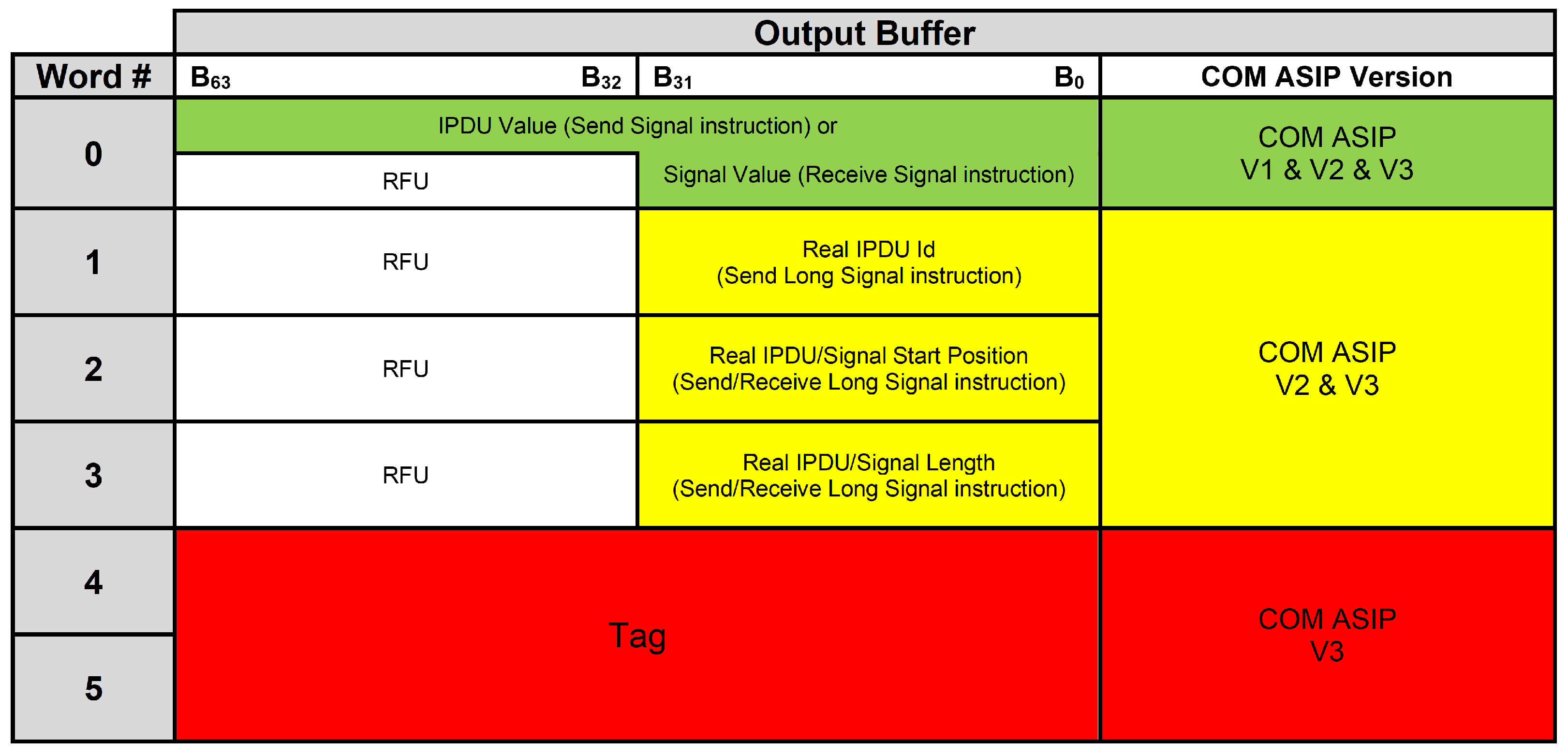
The output buffer component is activated to save outputs from the real IPDU Id Reg, the real IPDU/signal start position Reg, and the real IPDU/signal length Reg components.
2.1.12. Actions in Cycle 11
In cycle 11, a SW part of Com module can access the output buffer component. In case of a send signal/send long signal instruction, this SW part of the Com module can get, through the output buffer component, a final value for a PDU that corresponds to a currently processed virtual signal. In case of a receive signal/receive long signal instruction, this SW part can get, through the output buffer component, a current runtime value for a currently processed virtual signal from its corresponding PDU.
2.2. The GCM Hashing Algorithm
GCM [
13] is a highly secure algorithm that was published by the National Institute of Standards and Technology (NIST) in 2007 [
14]. It is currently implemented in many hardware security modules (HSMs) that are parts of many automotive micro-controller units (MCUs). Many papers have optimized implementations of GCM, increasing its throughput and the speed of its internal operations in application-specific integrated circuit (ASIC)-based architectures [
19,
20,
21,
22,
23] or field programmable gate array (FPGA)-based architectures [
24,
25,
26,
27,
28,
29,
30,
31]. GCM is also used in network-based systems to secure communication [
32,
33,
34,
35,
36,
37]. GCM has been used in automotive [
38] and IOT domains [
39,
40] as well.
GCM is used for authentication encryption with associated data. GCM provides three main features. The first feature is assurance of confidentiality of input data. This is achieved by encrypting input data using a variation of the counter mode operation of encryption [
41], which is a recommended block cipher mode of operation for an Advanced Encryption Standard (AES) [
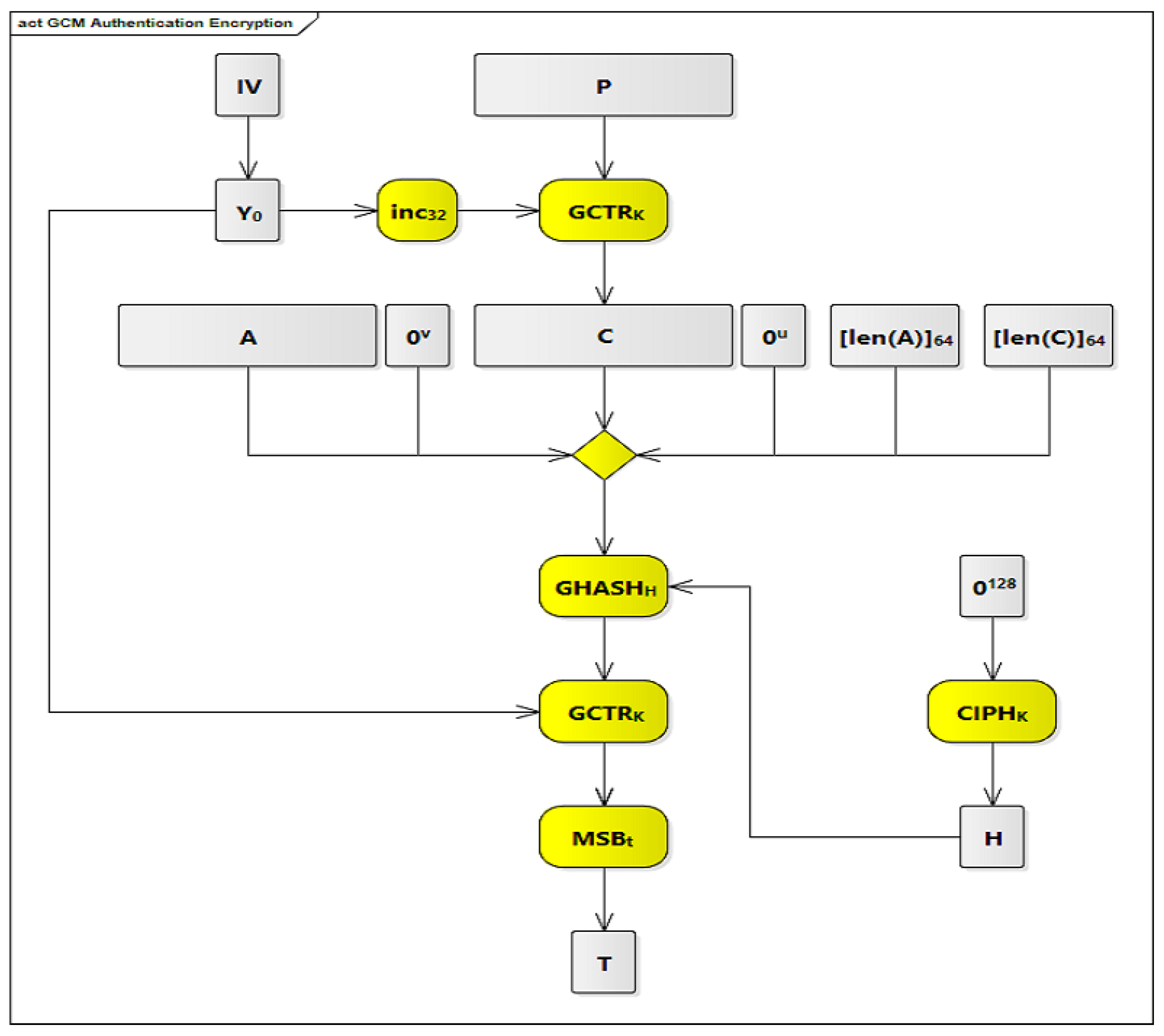
42]. The second feature is assurance of authenticity of confidential data from the previous feature. This is achieved by using a universal hashing function that is defined over a binary Galois (i.e., finite) field. The third feature is assurance of authenticity of additional data that are not encrypted. The GCM authentication encryption process is shown in
Figure 5 and
Figure 6. The symbols and processes shown in these figures are described in
Table 1.
In
Figure 5, there are 7 processes that are highlighted in yellow. The first process is the inc
function that is used to increment the pre-counter block (Y
) each time to generate a new counter block to be used with the GCTR
function.
The second process is the GCTR function near the top of the table. This process receives two inputs and produces one output. The two inputs are the plaintext P blocks and the counter blocks. The outputs are the ciphertext C blocks.
The third process is the CIPH function that is used to generate the hash subkey (H) from the zero block (0).
The fourth process is the yellow diamond in the middle of the table. This diamond is an aggregation function that aggregates six inputs. These inputs are the Additional Authenticated Data A; 0, which are 0 bits in length and appended to A; the ciphertext C blocks; 0, which are 0 bits in length u appended to C; [len(A)], which represents the length of A in bits; and [len(C)], which represents the length of C in bits.
The fifth process is the GHASH function that performs a multiplication operation between two inputs and produces one output. The first input is the aggregated data resulting from the fourth process (A 0 C 0 [len(A)] [len(C)]), and the second input is the hash subkey (H) resulting from the third process. The output from the fifth process is one of the inputs to the sixth process.
The sixth process is the GCTR function, shown near the bottom of the table. This process receives two inputs and produces one output. The first input is the output from the fifth process and the second input is the pre-counter block (Y). The output from the sixth process is the input to the seventh process.
The seventh process is MSB, which takes the most significant t bits of the provided input to produce the final tag T.
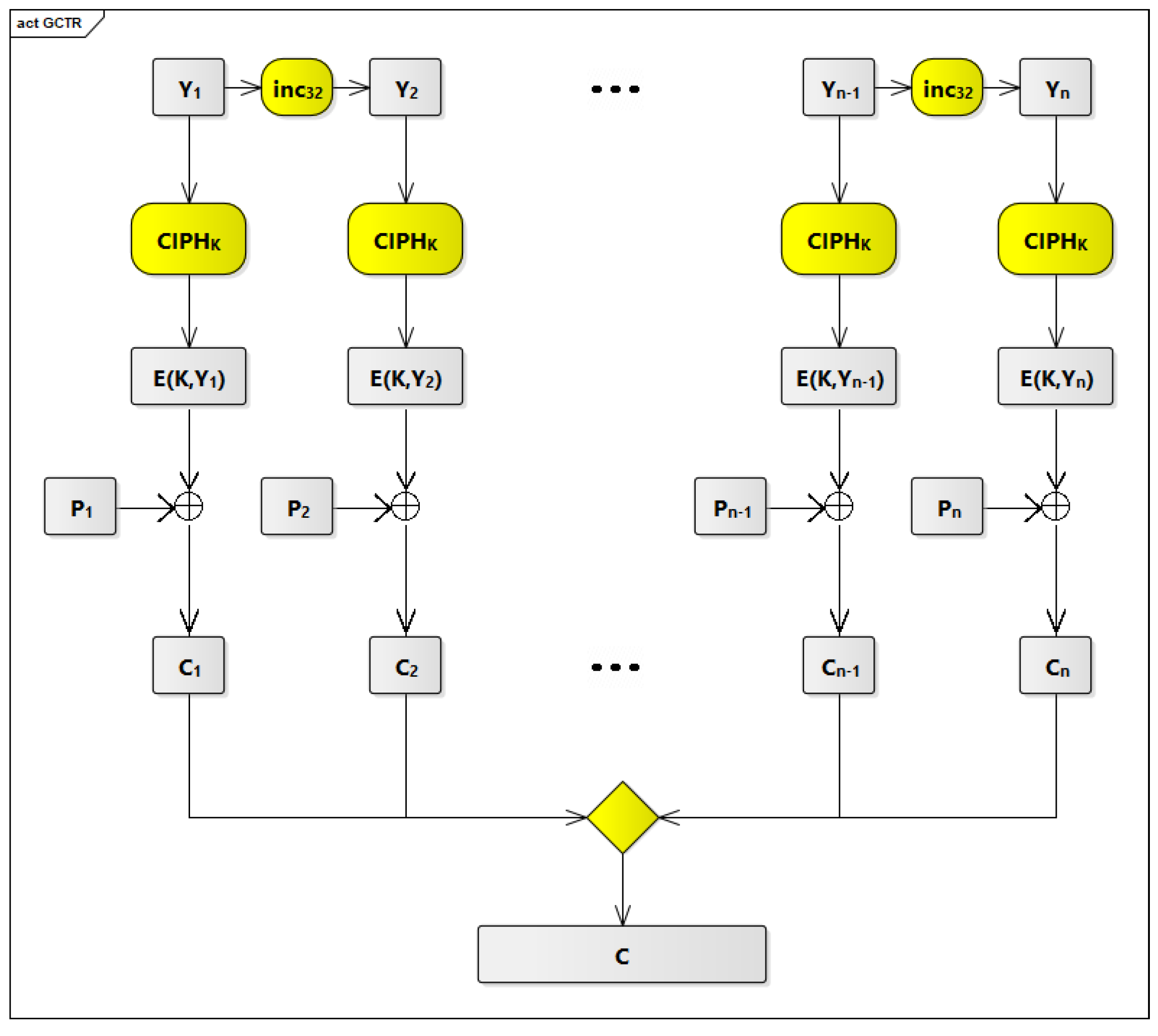
Figure 6 describes, in detail, the second process (i.e., GCTR
function on the top of
Figure 5). As described before, the GCTR
function receives two inputs and produces one output. The two inputs are the plaintext P blocks P
to P
and the counter blocks Y
to Y
. The GCTR
function applies the forward cipher function (CIPH
) to the second input (i.e., the counter blocks Y
to Y
) to produce the cipher counters E(K,Y
) to E(K,Y
). After that, the GCTR
function does exclusive-OR (XOR) operations between the cipher counters E(K,Y
) to E(K,Y
) and the plaintext P blocks P
to P
to produce the ciphertext C blocks C
to C
.
2.3. The Two-Layer Security Process Using GCM and COM ASIP
We introduced a two-layer process to increase the security of the GCM hashing algorithm. In order to use GCM with our COM ASIP, we analyzed three designs to construct plaintext. The first option is to consider each PDU as the plaintext that is an input to GCM. The second is to consider each signal as the plaintext that is an input to GCM. The third is the two-layer security process that is described in
Section 2.3.3 and
Section 2.3.4.
2.3.1. The First Design
For the first design, we need to divide each PDU into blocks of fixed length. The length of each block is 128 bits.
The First Difficulty
The first difficulty in this design comes from the fact that instructions supported by our COM ASIP work with signals but not with PDUs. Supporting this new design will require changing structure of our ASIP, introducing many new components and data paths, and changing the ISA of our ASIP completely, which will affect both the flexibility and performance of our ASIP.
The Second Difficulty
Another difficulty comes from the fact that signals differ from each other in their sizes and positions within PDUs. By dividing PDUs into 128-bit blocks, we might find that one signal, based on the position and size of this signal within its corresponding PDU, spans over two consecutive blocks, as shown in
Figure 7, where signal 3 spans over block 0 and block 1. This will also complicate our ASIP and affect its flexibility and performance. Based on the previous points, we discarded that design choice.
2.3.2. The Second Design
For the second design, we need to divide each signal into blocks of fixed length, where length of each block is 128 bits. A signal can fit into one block if its length is ≤128 bits. If the length of the signal is >128 bits, it is divided into more than one block. In both cases, padding is used, if it is necessary, to have complete blocks (i.e., length of input data is multiple of block length).
A Better Design
This design is better than the first design. The reason is that instructions supported by our COM ASIP already work with signals, so we do not need to introduce many changes in the structure of our ASIP. Although this design seems better than the first design, it has two main difficulties.
The First Difficulty
The first difficulty is that this design requires reserved bytes for each signal to contain its hash value, which will require transmitting much more data from sender ECUs to deliver hashes of such signals to receiver ECUs so receiver ECUs can verify such signals correctly. This will consume the bandwidth of communication buses that connect ECUs and will decrease the throughput of such communication buses to transmit actual data.
Table 2 shows the utilization percentage, to transmit actual data, of communication buses when we use different tag lengths. The original tag length is 128 bits, and truncated tag lengths can be smaller (16 bits, 32 bits, 64 bits, etc.). The red color indicates that the utilization percentage is less than 50%, the green color indicates utilization percentage is more than 50%, and the yellow color indicates utilization percentage is 50%. As we can see, the utilization percentage is less than 50% in most of cases, which impacts the throughput of the communication buses and affects the performance and usability of our design.
The Second Difficulty
The second difficulty is that we need to change the structure of the PDUs to have room to hold hash values for signals contained in these PDUs. We have two approaches. The first approach is to add these hash values to the ends of PDUs. The second approach is to allow each signal to have its own hash directly after its end, which requires shifting positions of the following signals in this PDU and changing the structure of this PDU completely. Both problems, as we can see, affect the performance and flexibility of this design choice, so we discarded this design choice as well.
2.3.3. The Third Design
The third designis similar to the first design. We consider each PDU as the plaintext that as an input to the GCM, and there is only one hash value for each PDU. The difference is that we do not divide each PDU into blocks of fixed length. Instead, we consider each virtual signal in these PDUs as one block, and padding is used to complete the block. The next signal in this PDU is considered as the next block in this plaintext, the third signal is considered as the third block in this plaintext, etc.
The First Layer of Security
The first layer of security in this design comes from GCM itself, as any attacker needs to know IV and K to bypass the authenticity of the transmitted data and alter them if needed.
The Second Layer of Security
The second layer of security comes from the fact that even if any attacker breaks the first layer of security by knowing IV and K, he will not be able to use them to alter a transmitted PDU. This is because he also needs to know how signals are placed inside these PDUs, which differs based on positions and sizes of signals inside these PDUs, from one PDU to another.
More Security
Based on the previous points, attackers also need to know positions and sizes of all signals inside ECUs to be able to break the second layer of security, which is much more complex than using only one layer of security.
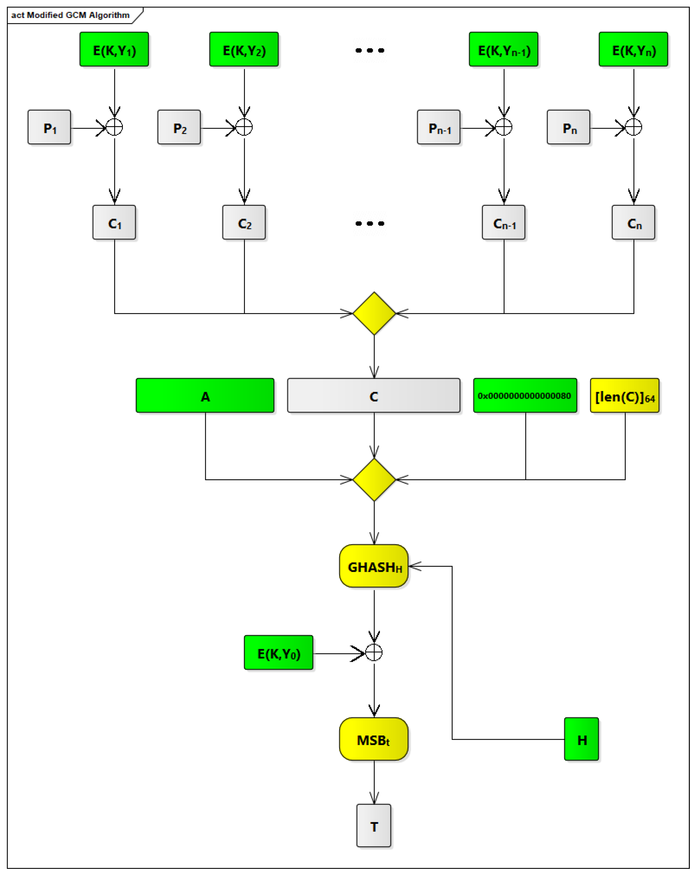
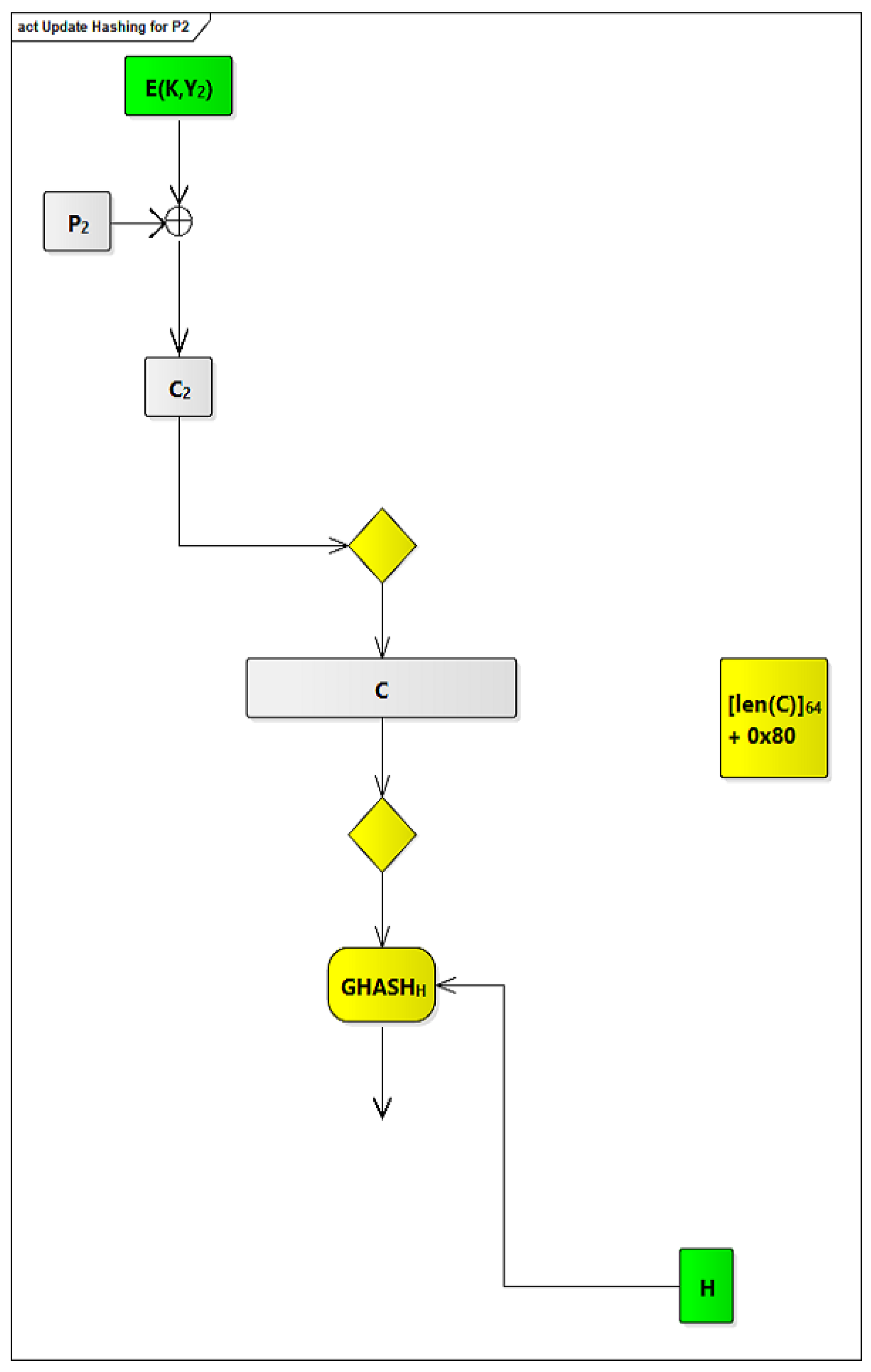
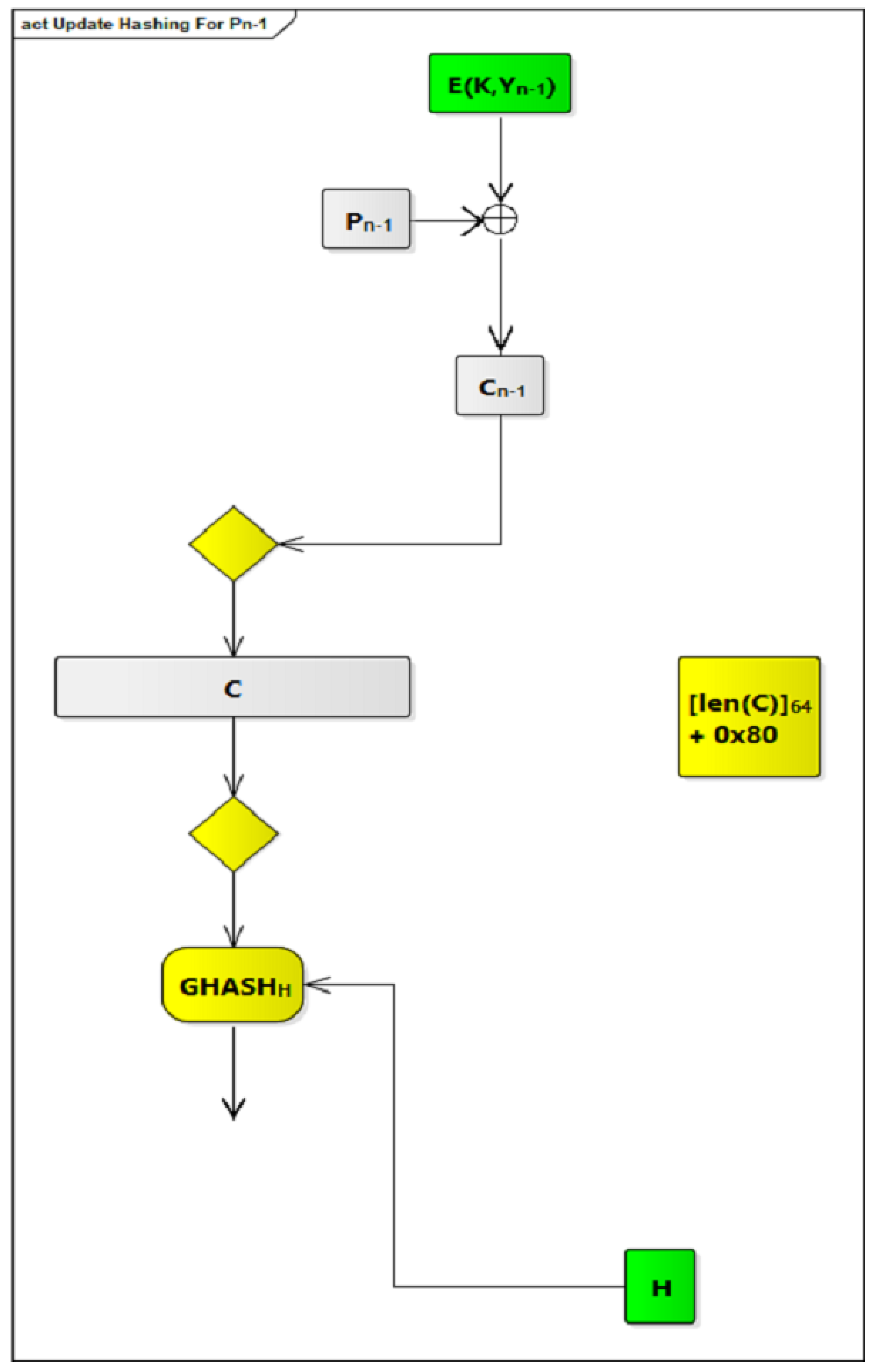
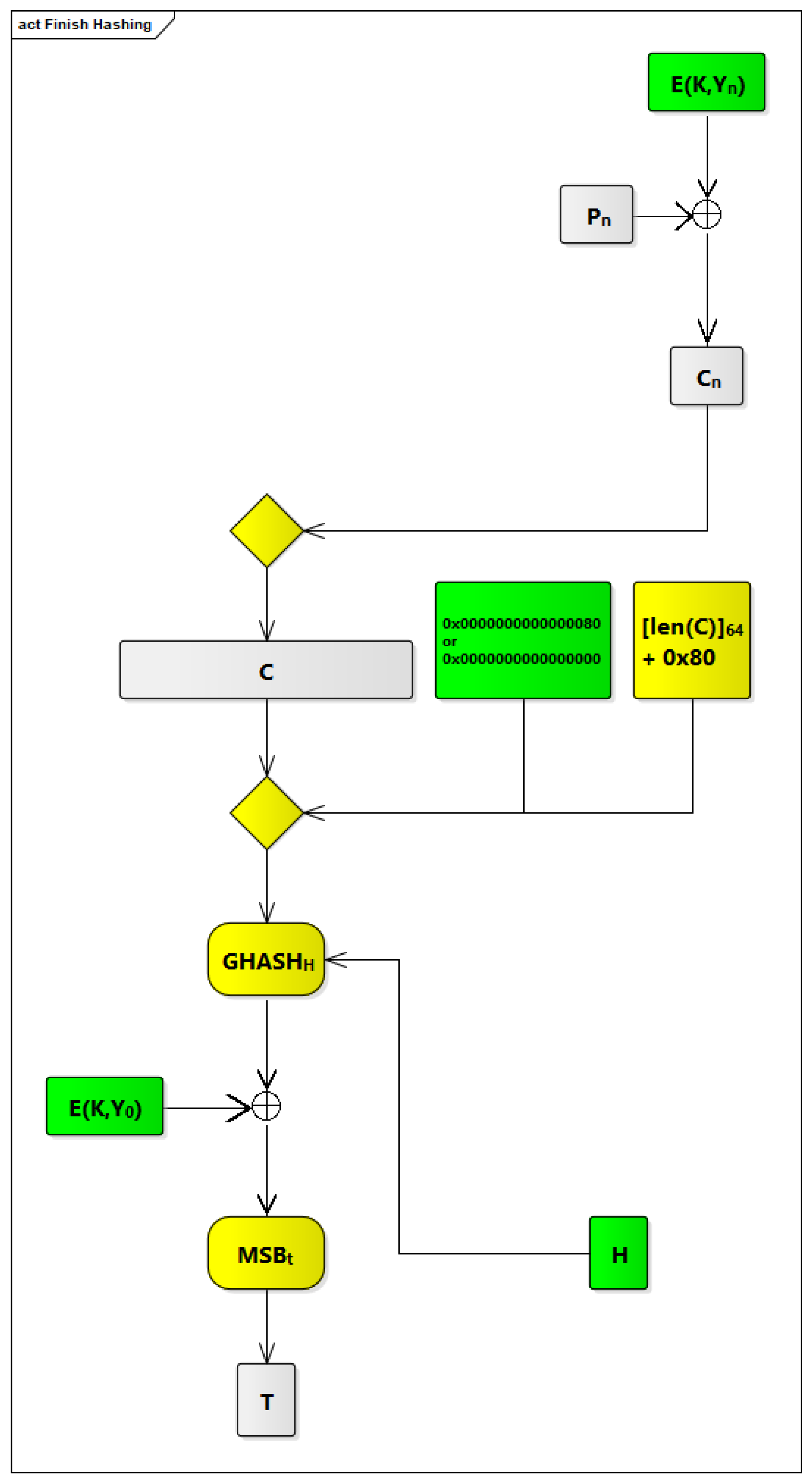
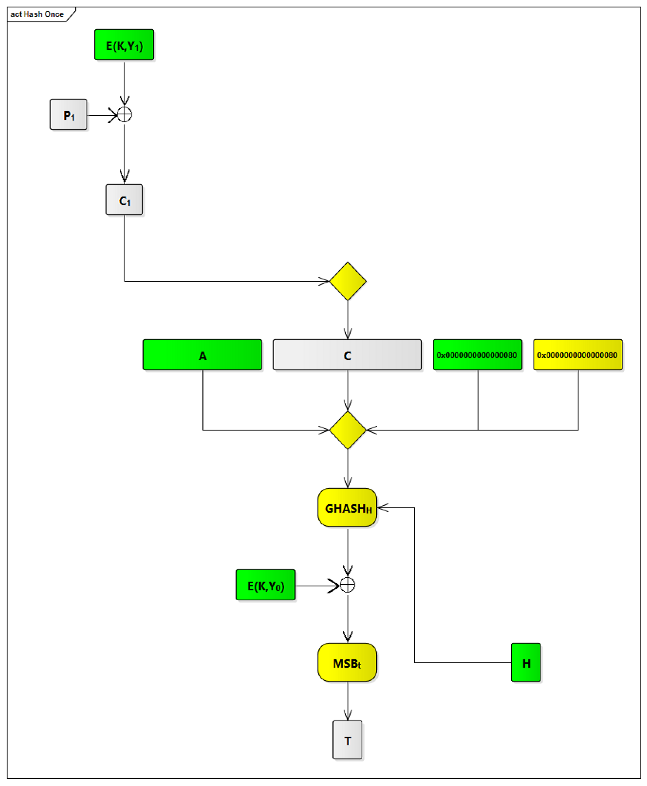
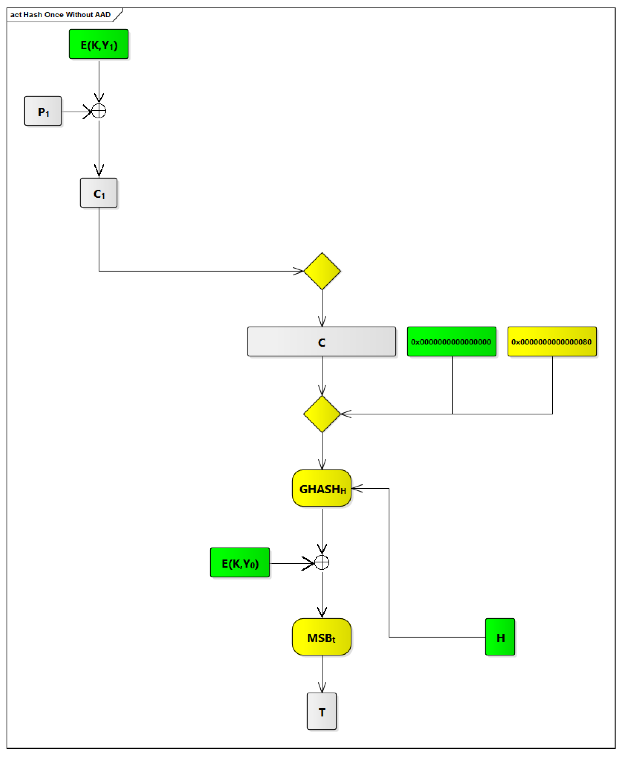
2.3.4. The Modified GCM Algorithm
In order to integrate GCM within our COM ASIP, we have made some modifications to the original GCM to make it faster. The modified GCM algorithm is shown in
Figure 9. The modifications that we have been made are based on identifying possible processes, in the original GCM algorithm, which can be done offline.
The First Offline Process (Generating Y from IV)
The first process is generating Y from IV. This process has to be done online in case IV can be changed. In the context of our COM ASIP, IV is static and has a fixed length, 96 bits, so converting IV to Y can be done offline, and Y is saved in a secure memory component that is part of our ASIP.
The Second Offline Process (Generating E(K,Y))
The second process applies CIPH
to Y
. This process (i.e., E(K,Y
)) is part of the GCTR
process that is applied to the output from the GHASH
process. In the context of our COM ASIP, Y
is static because IV is static, so E(K,Y
) is static as well and can be done offline. E(K,Y
) is saved in a secure memory component that is part of our ASIP. Based on the previous points, the GCTR
process that is applied to output from GHASH
process will turn out to be an XOR operation between E(K,Y
) and output from the GHASH
process. This is shown in
Figure 9.
The Third Offline Process (Incrementing Y and Generating Y to Y)
The third process is incrementing Y to generate counters, Y to Y, which is used as inputs to the GCTR process that is applied to plaintext blocks. This process can be done offline, and these counters, Y to Y, is saved in a secure memory component that is part of our COM ASIP.
The Fourth Offline Process (Generating E(K,Y) to E(K,Y))
The fourth process is applying CIPH
to counters Y
to Y
. This process (i.e., E(K,Y
) to E(K,Y
)) is part of the GCTR
process that is applied to plaintext blocks. In the context of our COM ASIP, Y
to Y
are static because Y
is static, so E(K,Y
) to E(K,Y
) are static and can be performed offline. E(K,Y
) to E(K,Y
) is saved in a secure memory component that is part of our ASIP. Based on the previous points, the GCTR
process that is applied to plaintext blocks will involve XOR operations between plaintext blocks (i.e., P
to P
) and E(K,Y
) to E(K,Y
). This is shown in
Figure 9. To simplify the design of our ASIP and increase its efficiency and operability, counters are limited to 64 counters, from Y
to Y
, to reduce the size of secure memories that is used to save these counters (i.e., Y
to Y
) and their corresponding cipher values (i.e., E(K,Y
) to E(K,Y
)).
The Fifth Offline Process (Calculating the Length of AAD)
The fifth process is calculating the length of AAD. In the context of our COM ASIP, AAD is only one block (i.e., its length is 128 bits), so it has a fixed length, and [len(A)
] can be replaced, as shown in
Figure 9, by a static value (i.e., 0x0000000000000080).
The Sixth Offline Process (Appending vs. Bits to AAD)
The sixth process is appending vs. bits to AAD. This process (i.e., 0) was eliminated, as the length of AAD is ma ultiple of block length (i.e., length of AAD is 128 bits, which corresponds to one block).
The Seventh Offline Process (Appending u Bits to C)
The seventh process is appending u bits to C. This process (i.e., 0
) was eliminated, as the length of C is a multiple of block length. We ensured this because, based on the third design in
Section 2.3.3 that we selected, each virtual signal is considered as one plaintext block, and each PDU contains a number of virtual signals, so we have a number of complete blocks that represents this PDU.
The Eighth Offline Process (Generating H)
The eighth process is generating H from the zero block. The zero block (i.e., 0) is static, so H (i.e., E(K,0)) is static as well. Thus, generating H from the zero block can be done offline, and H is saved in a secure memory component that is part of our COM ASIP.
The Modified GCM Algorithm
Based on the previous offline processes, we modified the original GCM algorithm, and our modified design, as shown in
Figure 9, is integrated within our COM ASIP. This modification is described in
Section 2.4. In
Figure 9, the components and processes that are done offline are highlighted in green, and those that are done online are highlighted in yellow.
Secure Memory Components Are Needed
Based on those offline processes, we concluded that we need secure memory components. These memory components are used to save Y
, E(K, Y
), and Y
to Y
; and E(K,Y
) to E(K,Y
) and H. Y
and Y
to Y
can be removed from these secure memory components because they will not be used directly, as shown in
Figure 9, in our modified GCM algorithm. The only secure memory components that are needed are those that are used to save E(K, Y
) and E(K,Y
) to E(K,Y
) and H.
2.5. The Additions to COM ASIP ISA to Support the Hashing Instructions
The additions to COM ASIP V2 to support the hashing instructions are shown in
Figure 18. For the previous send long signal and receive long signal instructions, no changes in instruction flow during the twelve execution cycles are needed. These instructions (i.e., the send long signal and the receive long signal instructions) work without any extra logic to handle them in COM ASIP V3. For the hashing instructions, the changes in instruction flow are illustrated below.
2.5.1. Changes in Cycles 0, 1, 2, 3, 4, and 5
In cycles 0, 1, 2, 3, 4, and 5, no changes are expected.
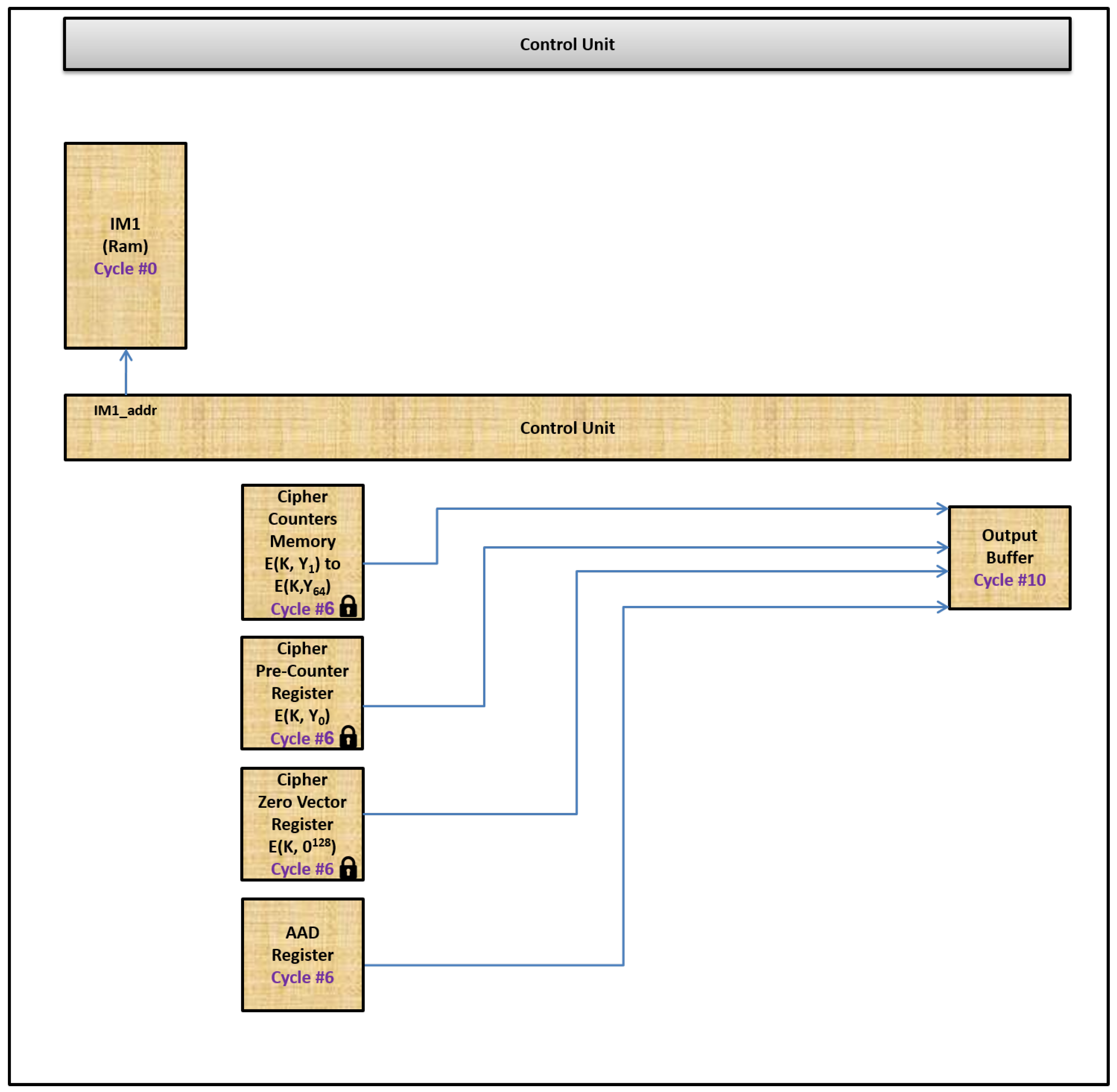
2.5.2. Changes in Cycle 6
In cycle 6, the control unit component checks which hashing instruction is currently being executed. It activates, based on the hashing instruction, the needed memory components to read a word from each of them.
Table 4 shows which memory components that will be activated.
2.5.3. Changes in Cycle 7, 8, and 9
In cycle 7, 8, and 9, no changes are expected.
2.5.4. Changes in Cycle 10
In cycle 10, the output buffer component is activated to apply the GHASH process, using the inputs received from cycle 6, to update a tag value that should be appended to a given PDU. Upon executing a finish hashing, hash once, or hash once without AAD instruction, a final tag value for a PDU that is currently processed is placed in the output buffer component.
2.5.5. Changes in Cycle 11
In cycle 11, no changes are expected.


