Article

A 3rd-Order FIR Filter Implementation Based on Time-Mode Signal Processing

by
Orfeas Panetas-Felouris
* and
Spyridon Vlassis
Electronics Laboratory, Physics Department, University of Patras, 26504 Patras, Greece
*
Author to whom correspondence should be addressed.
Electronics 2022, 11(6), 902; https://doi.org/10.3390/electronics11060902
Submission received: 28 January 2022 / Revised: 10 March 2022 / Accepted: 11 March 2022 / Published: 14 March 2022

Abstract

:
This paper presents the hardware implementation of a 3rd-order low-pass finite impulse response (FIR) filter based on time-mode signal processing circuits. The filter topology consists of a set of novel building blocks that perform the necessary functions in time-mode including z−1 operation, time addition and time multiplication. The proposed time-mode low-pass FIR filter was designed in a 28 nm Samsung fully-depleted silicon-on-insulator FD-SOI process under 1 V supply voltage with 5 MHz sampling frequency. Simulation results validate the theoretical analysis. The FIR filter achieves a signal-to-noise-plus-distortion ratio (SNDR) of 38.6 dB at the input frequency of 50 KHz consuming around 200 μW.

1. Introduction

In many modern integrated circuit applications, better speed and lower power consumption are important criteria. Because of the reducing device sizes and low voltage supply, these criteria are met utilizing cutting-edge complementary metal-oxide-semiconductor (CMOS) technologies. Unfortunately, due to smaller device sizes and low power supply, many prior analog circuit architectures, such as analog-to-digital converters, are more difficult to overcome the lower voltage headroom and the lower dynamic range
The time-domain technique is a relatively recent method of processing time that utilizes time delay, time difference or pulse width rather than voltage or current, as in traditional processing methods. As a result, in time-domain circuits and systems, time is the quantity of interest [1,2,3]. Even for such a scaled technology, time-domain design is a very promising design method since it offers a better trade-off between dynamic range and power consumption. The advantage of time-domain systems is that they use high-speed MOS devices, which means they have a shorter time delay and so process time with more precision [4,5,6].
The main advantages of the time-domain design approach are improved dynamic range and time resolution when compared to analog voltage or current mode circuits under the same low-supply environment [4,5,6] and better power efficiency for high-speed performance because they are primarily composed of CMOS digital building blocks (gates, etc.) [1].
Signal filtering is one of the most important functions in many state-of-the-art applications, such as biomedical sensor interfacing, image processing, wireless receivers, etc. Signal filtering, which is based on finite/infinite impulse response filter implementation (FIR/IIR), belongs among the basic signal processing operations in traditional discrete-time digital signal processing (DT-DSP).
FIR/IIR implementations require some fundamental operators, such as z−1 operators and signal adders, along with signal multipliers, for the implementations of the filter coefficients. Traditional FIR/IIR implementations are mainly based on pure digital design approach and, therefore, can be categorized as discrete-time/discrete-signal processing systems. The circuit realization of the basic operators is achieved using flip-flops as delay element and digital logic gates for the implementation of the digital logic adders and multipliers.
The FIR/IIR counterpart implementations in time-mode require the basic operators to work in time domain which means that z−1, adders [4,7,8] and multipliers [9,10] must be able to handle time-mode quantities [11]. These systems are categorized as discrete-time/continuous signal processing (DT-CSP) systems [12].
Few works about time-mode FIR/IIR or other time-mode filter implementations have been reported in the literature. A 2nd-order Butterworth and Chebyshev Type I time-mode filters have been presented in [13]. These implementations are based on time-mode signal processing circuits, which, unfortunately, cannot be used as separate modules leading to complicate configurations. A set of time-mode building blocks used to build a sampled-data 2nd-order low-pass IIR filter along with the methodology for the construction of higher-order systems are presented in [14]. A 3-tap FIR filter and a new way of analog computation using novel time-mode operator circuitries are presented in [12].
Our work proposes the implementation of a 3rd order sampled-data low pass time-mode FIR filter which is based on the novel time-mode multiplier and time-mode adder. Both circuits are based on the modification of a simple time register topology [15,16]. A 3rd order low-pass topology offers a satisfactory trade off between high-frequency rejection, chip area and current consumption. The proposed time-mode operators feature several advantages leading to robust FIR filter implementation: (a) low circuit complexity including few transistors, (b) high accuracy in time storing (c) synchronization with the reference sampling clock and (d) modular design. The main advantage of the proposed time-mode FIR compared with aforementioned state-of-the-art works is that it can be easily realized based on the topological diagram of the traditional FIR approach in voltage mode and substituting one-by-one the voltage-mode operators with the time-mode counterpart modular operators.
The paper is organized as follows. A brief presentation about time-mode signal processing and the definition of the time-mode operators presented in Section 2. The circuit modifications of the time register in order to build the multiplier and adder operators are described in Section 3. In Section 4, the proposed time-mode modules are presented and analyzed, while the FIR filter is analyzed in Section 5. The simulation results are reported in Section 6.

2. Time-Mode Signal Processing

The time-mode circuits and systems process the time difference between two consecutives pulses or the time width of a constant frequency pulse. This work will focus on the time processing approach that handles the pulse width of a constant frequency pulse. In 
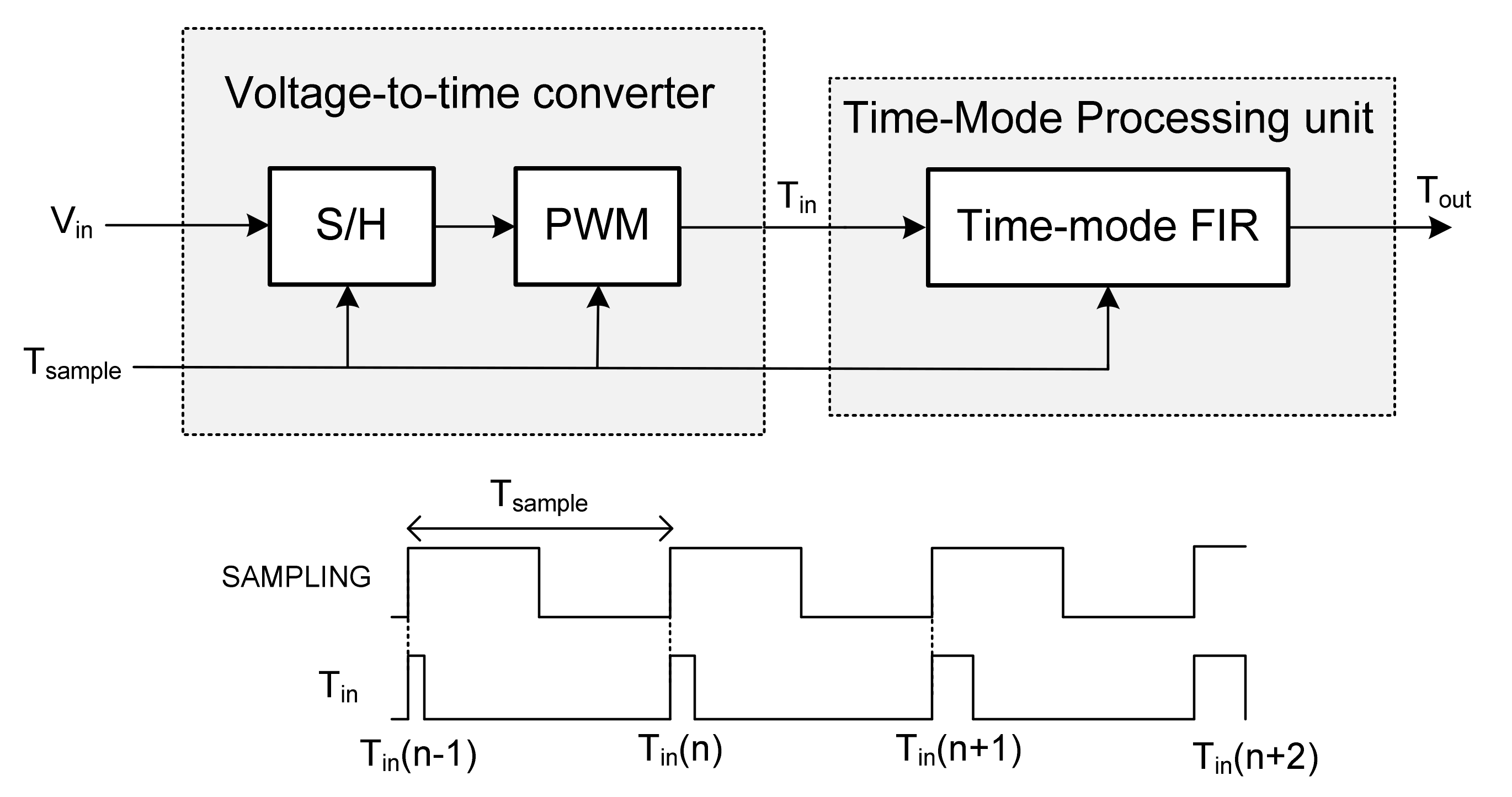
Figure 1, a conceptual block diagram is presented.
The input signal Vin is converted to time-mode by using a sample/hold stage (S/H) and pulse width modulator (PWM). S/H is necessary for high-frequency input bandwidth and can be omitted for low-frequency input signals (e.g., signal which comes from sensor interfacing circuit). Based on the PWM technique, input voltage Vin will correspond to an input pulse width Tin of a constant frequency pulse [2,17] according to the next equation:
T i n n = k V T V i n n
where kVT is the voltage-to-time conversion factor, and n is the number of sample, while the constant frequency is assumed the sampling frequency fsampling. It is clear that Tin can take continuous values according to Equation (1), but the time is discrete by mean of sampling time, and the corresponding system is considered a DT-CSP system [12]. Afterward, the signal is processed by the main time-mode systems, which is capable of handling the pulse widths of a pulse train.
One of the major building blocks embedded in continuous or discrete signal processing is the filters: analog filters or FIR/IIR filters. Despite implementation, filters must be capable of filtering out all the unwanted signals/components, which are corrupted with the signal or bandwidth of interest. From the time-mode point of view, any filter implementation is similar to FIR/IIR discrete filters mainly due the use of discrete sampling time.
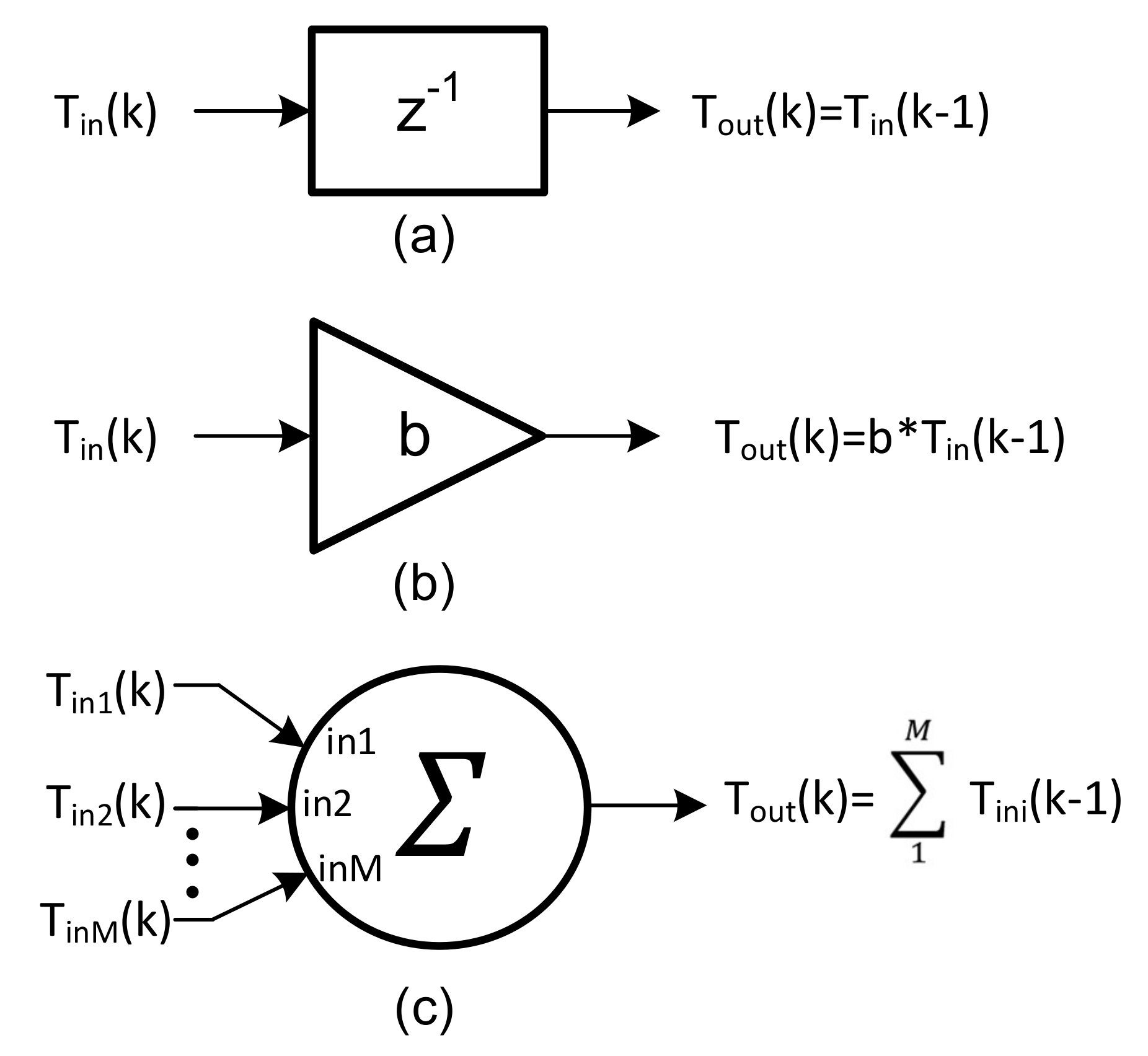
This study will concentrate on the implementation of time-domain FIR filters. A FIR filter is a signal processing filter whose impulse response (or response to any finite length input) has a limited duration since it settles to zero in a finite time. Each value in the output sequence for a causal discrete-time time-mode FIR filter of order N is a weighted sum of the most recent input values [18]:
T O U T n = b o T i n n + b 1 T i n n 1 + + b N T i n n N = i = 0 N b i T i n n i
where
  • Tin[n] is the input pulse width;
  • Tout[n] is the output pulse width;
  • N is the filter order;
  • bi is the filter’s coefficient at the i-th instant for 0 ≤ iN of an Nth-order FIR filter.
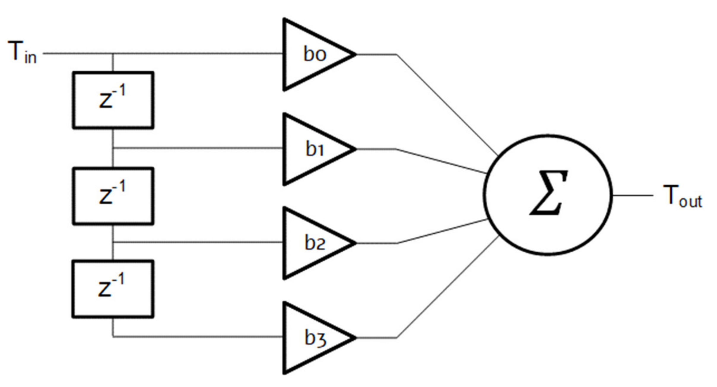
Therefore, the most important operators in the corresponding time-mode FIR filters will be the time-mode z−1 operators, time-mode multiplier and the time-mode adders. The block diagram of these operators in the time-mode are presented in Figure 2. The circuit implementations of the aforementioned operators will be described in the next sections.

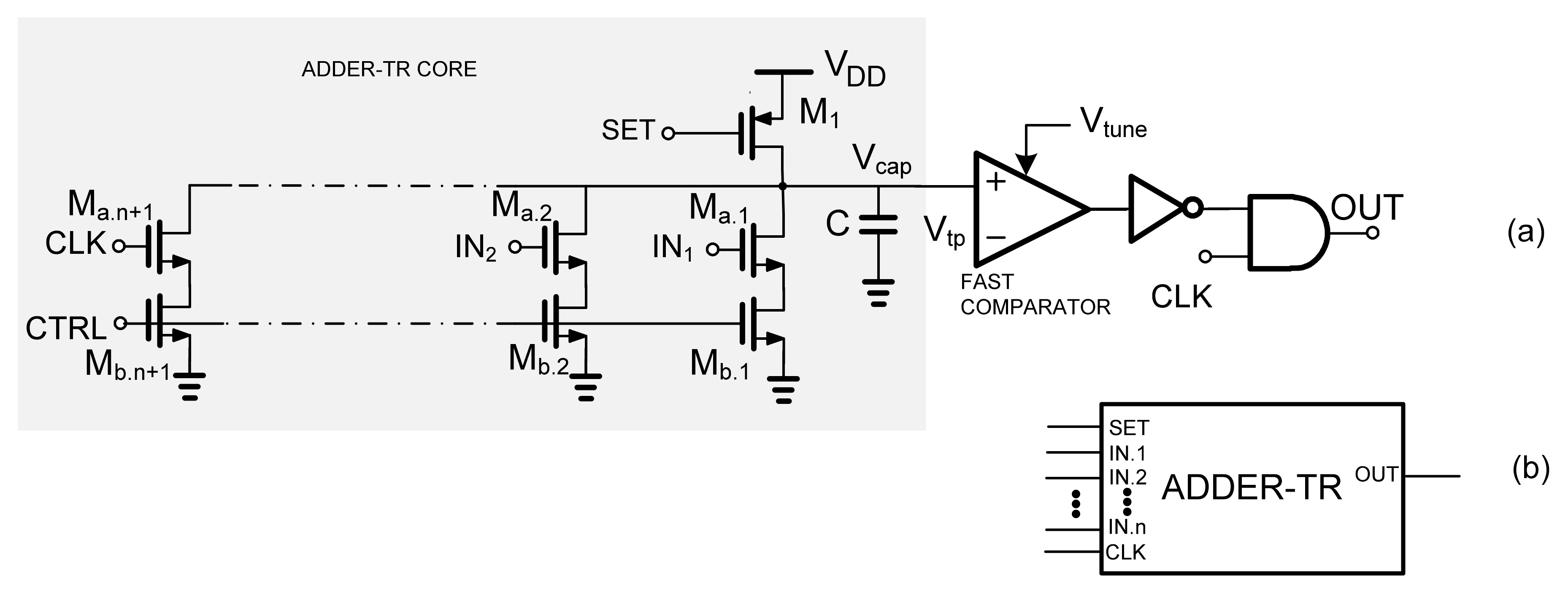
3. Multiplying and Adding Operations of the Time Register

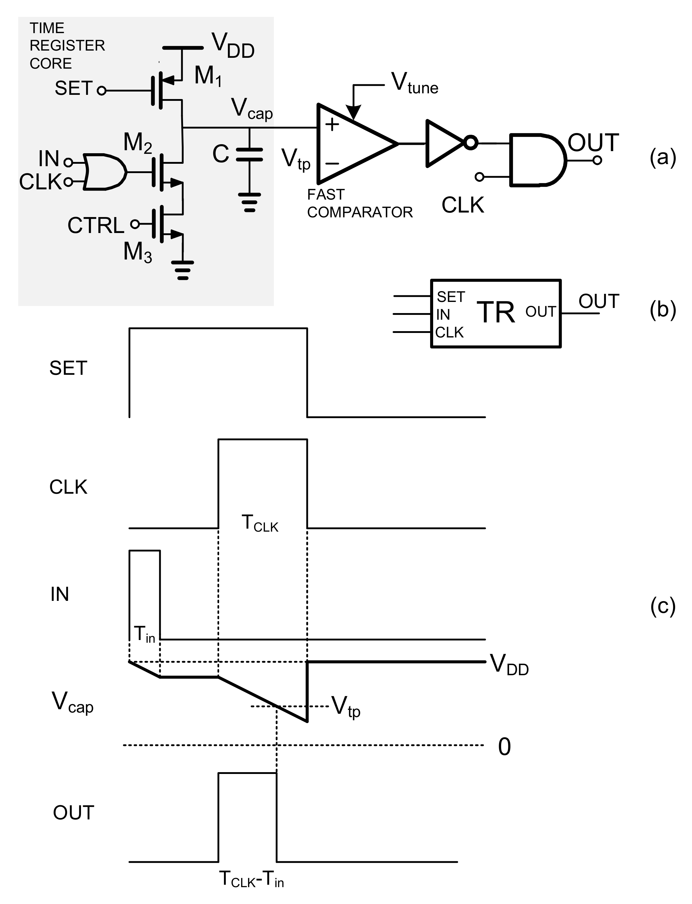
Figure 3a shows the time register (TR), and Figure 3b shows its symbol. When SET = 0, transistor M1 is turned on, and the capacitor voltage is set to VDD (supply voltage). Τhe capacitor discharges when transistor M2 is ON, which is controlled by the OR gate. Through a digital calibration loop, the M3′s gate voltage CTRL may be utilized to calibrate the variance of the discharging slope [16]. To synchronize the output with CLK, the synchronization circuitry consists of an AND gate, a fast comparator [16] and an inverter. The comparator is designed to provide quick transient response, and its triple point voltage Vtp is set to match VDD/2 [16].
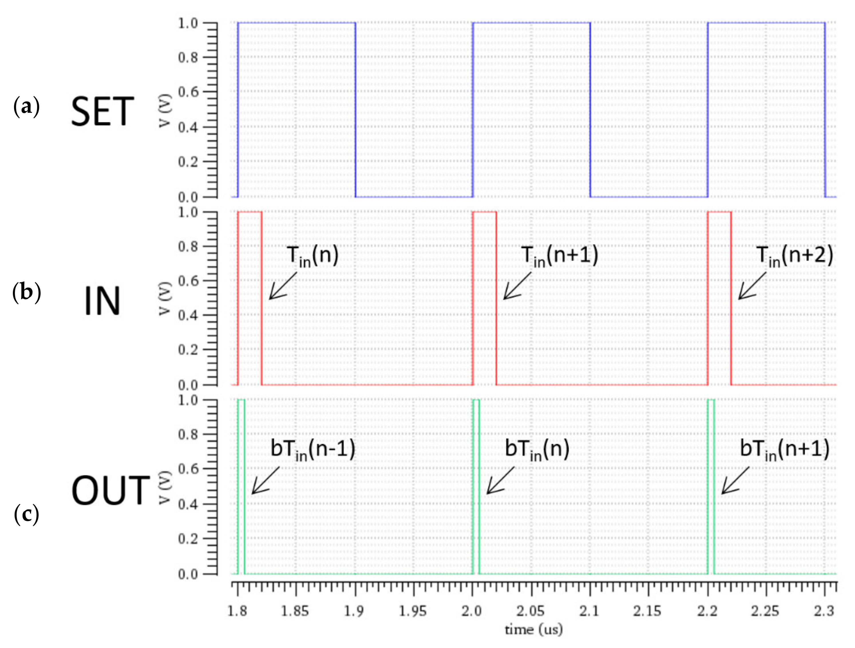
Figure 3c shows a time diagram of a time register that describes the synchronization procedure. The SET signal’s time interval TCLK is a pulse with a fixed pulse width and a 25% duty cycle. The capacitor voltage remained constant when both IN and CLK are 0. The larger the pulse width Tin of the IN signal, the more discharging time due to Tin appeared, considering that the discharging time due to CLK stays the same.
The output is a pulse with width equal to TCLKTin, allowing the value of Tin to be stored, while the output pulse is synchronized with the CLK signal.
Using the aforementioned time register circuit, the circuit can store the time interval of an input pulse and amplify the pulse width by a gain factor. The new circuit is called time amplifier and is presented in Figure 4. In this configuration, the operation of the OR gate is performed by the two-transistor branches Ma1Mb1 and Ma2Mb2. Transistors Ma1 and Ma2 have the same aspect ratio acting as switches. The aspect ratios of Mb1, Mb2 are different, featuring a different discharging slope. Assuming that the channel widths of Mb2 and Mb1 are Wb.2 and Wb.1, respectively, while both transistors have the same channel length. Then, intuitively, using Figure 3c, the discharging slope between Tin and TCLK will be different. The discharging slopein that corresponds to Tin will be given by
s l o p e i n = a s l o p e c l k
where a is the time gain and is given by
a = W b .2 W b .1
and slopeclk is the discharging reference slope caused by TCLK. Therefore, the output pulse width will be equal to
T O U T = T C L K W b .2 W b .1 T i n
A time adder circuit, which is based on the time register, is presented in Figure 5. A time adder simply adds the pulse widths Tin.1, Tin.2, …, Tin.n of n number input pulses. Transistors Mb.1, Mb.2 …, Mb.n, Mb.n+1 have the same aspect ratio. Therefore, the discharging slope caused by Tin.1, Tin.2, …, Tin.n will be given by
s l o p e i n .1 , i n .2 , , i n . n = s l o p e i n .1 + s l o p e i n .2 + s l o p e i n . n
and the output pulse width will be
T O U T = T C L K ( T i n .1   + T i n .2   +   T i n . n )
The main problem of the time register is the strong impact of the technology process (P) variations and chip temperature (T) variation (PT variations). The discharging slope of the capacitor voltage discharging shows variation over PT variations because of its dependency by the discharging drain current of a MOS device and the value on-chip capacitor. A digital calibration loop can be used in order to calibrate the discharging slope achieving better performance stability [16].

4. Time-Domain Modules

4.1. Time-Domain z−1 Circuit

The operation of the z−1 is to generate an output pulse with pulse width equal to Tin, which is synchronized with the sampling [16]. As discussed in the previous section, unfortunately a TR circuit can store the pulse width Tin of the input (IN)signal in the form of output pulses with pulse width equal to TCLKTin, which is synchronized with CLK.
The proposed z−1 circuit is presented in Figure 6a, and the basic waveforms that explain its operation are illustrated in Figure 6b,c. A combination of four TR circuits in series realizes a z−1 circuit. The SAMPLING signal is assumed to be the SET1 signal of the TR1 circuit, and the input signal IN is equal to the input IN1 of TR1, while the final output signal OUT is the output of OUT4 of TR4.
To be synchronized with the SET2 pulse, the OUT1 pulse is generated at the rising edge of CLK1. After that, the OUT1 was used as the TR’s input. OUT2 is synchronized with CLK2, and TOUT2 = TCLK − TOUT1 = TCLK − (TCLK + Tin) = Tin. Therefore, OUT2 is delayed by TSAMPLING/2 in relation to the sampling signal. Based on the previous characteristic, the OUT4 pulse is delayed by TSAMPLING and its width value is Tin. Taking this into account, the z−1 operator is produced by utilizing four TR in a cascade placement.

4.2. Time-Mode z−1 Multiplier

The operation of a time-mode z−1 multiplier is to produce an output pulse with pulse Tout width equal to bTin, where Tin is the input pulse and a is the multiplication coefficient, and the output pulses will be synchronised with the sampling signal and delayed by one clock cycle.
The proposed time-mode z−1 multiplier is presented in Figure 7a. The pulses timing diagram that explains its operation is illustrated in Figure 7b. Moreover, the clock’s timing diagram is the same as that of time-mode z−1 circuit as it is illustrated in Figure 6. The combination of two AMP-TR and two TR circuits series realizes a time-mode z−1 multiplier. The SAMPLING signal is assumed to be the SET1 signal of the AMP-TR1 circuit, and the input signal IN is equal to the input IN1 of AMP-TR2, while the final output signal OUT is the output of OUT4 of TR2. AMP-TR1 and AMP-TR2 generate time amplification equal to a1 and a2, respectively.
The OUT1 pulse is generated at the rising edge of CLK1 in order to be synchronized with the SET2 pulse. Afterwards the OUT1 was used as input for the TR1. So, TOUT2 = TCLKTOUT1 = TCLK − (TCLKa1Tin) = a1Tin, and OUT2 is synchronized with CLK2. Therefore, OUT2 is delayed by TSAMPLING/2 in relation to the sampling signal. Expanding on the previous characteristic, OUT4 is delayed by TSAMPLE, and the synchronized output pulse features a pulse width that is given by
T O U T = b T i n
where the multiplication coefficient will be equal to b = a1a2.
It should be mentioned here that the use of two-time amplification operations through the standard time-mode z−1 multiplier operation is very important. We have more degrees of freedom for the approximation of the FIR filter coefficient by using the product of two amplifications a1.a2, compared with the single amplification a1 or a2.

4.3. Time-Mode z−1 Adder

The time-domain z−1 adder can add the pulse width of several input signals and produce an output that is the sum of all the input time intervals. As an example, a two inputs time-domain z−1 adder is depicted in Figure 8a. The z−1 adder consists of ADDER-TR1 and three time registers (TR) in series. The pulses timing diagram that explains its operation is illustrated in Figure 8b. Again, the clock’s timing diagram is the same as that of the time-mode z−1 circuit as it is illustrated in Figure 6c.
The OUT1 pulse is generated at the rising edge of CLK1 in order to be synchronized with the SET2 pulse and has the value of TOUT1 = TCLK − (Tin1 + Tin2). Afterwards, the OUT1 was used as input for the next TR. So, TOUT2 = TCLKTOUT2 = TCLK −(TCLK − (Tin1 + Tin2) = Tin1 + Tin2, and OUT2 is synchronized with CLK2. Therefore, OUT2 is delayed by TSAMPLING/2 in relation to the sampling signal. Then, the signal just passes through the next two TRs in order to acquire a delay of one cycle. The pulse width of the output pulse will be given by
T O U T = T i n 1 + T i n 2
and, therefore, the adding function is realized.

5. Time-Domain 3rd Order FIR Filter

In this work, a rectangular 3rd-order FIR filter had been designed in order to prove the concept of time-mode filtering using the proposed time-domain z−1 multiplier and adder. The realization follows the topology of Figure 9, which uses three z−1 operators, four z−1 multipliers and one 4-input z−1 adder. Table 1 shows the ideal filter coefficients, the approximation values and the final coefficient realizations. As was already mentioned, the use of two amplification operations can help in the better approximation of the filter coefficients. Only three gain amplifier factors are necessary, 0.3, 0.4 and 0.7, in order to approximate the exact coefficient values of b0, b1, b2 and b3. The worst-case approximation error is less than 10%.

6. Results

In the following section, the performance of the proposed circuits is presented. All circuits are designed and verified by simulation in Samsung 28 nm FD-SOI CMOS technology with a supply voltage VDD = 1 V. The voltage triple point of comparator was adjusted to be 0.5 V using an appropriate triple-point compensation circuitry [15]. Considering that the input pulse width Tin is varied as a sinusoid, the maximum allowable peak-to-peak amplitude Tin.pp.aval can theoretically be equal to TCLK, which is equal to 50 ns in our implementation. As long as Tin.pp is close to TCLK then shorter pulses are generated inside z−1 circuit increasing the signal distortion. Therefore, a maximum peak-to-peak input amplitude Tin.pp.max of 40 ns is satisfactory, covering 80% of the maximum available range of 50 ns.

6.1. Time-Mode z−1 Multiplier

The operation of the z−1 multiplier is shown in Figure 10. Timing waveforms for a z−1 multiplier for a multiplying coefficient are equal to 0.28, (a) synchronization clock, (b) input pulses width with Tin = 20 ns and (c) output pulses with pulse width Tout = 5.55 ns. In Figure 10a, the synchronization clock is presented. In Figure 10b,c, the input and output pulses are presented, respectively. The input pulse width Tin is 20 ns, while the multiplier coefficient is chosen to be equal to 0.28. As a result, the circuit generates output pulses with a pulse width of Tout = 5.55 ns, as expected. In 
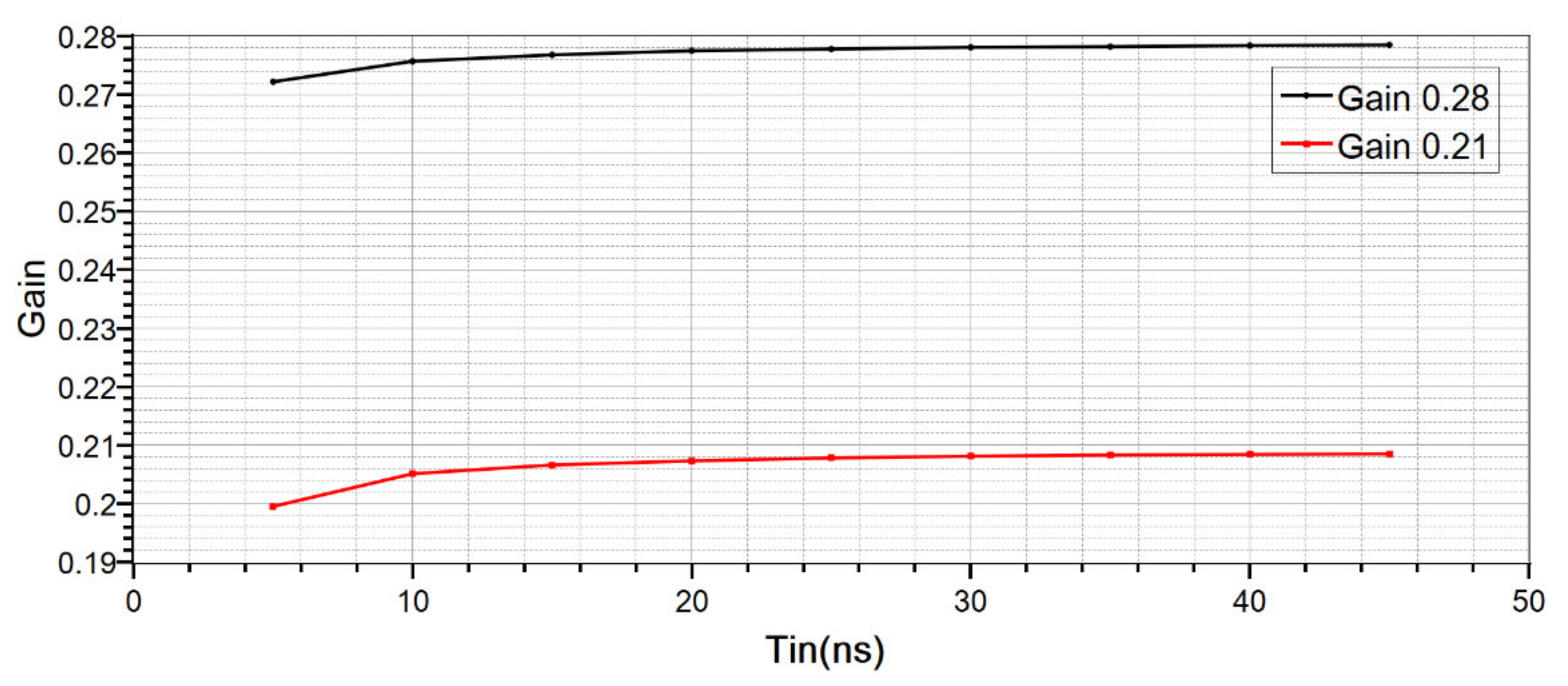
Figure 11, two cases of multiplication coefficient, with nominal values of 0.28 and 0.21, are presented in relation to the input pulse width. In the worst-case scenario of Tin.pp = 40 ns, the relative inaccuracy of the multiplication coefficient is less than 5%.

6.2. Time-Mode z−1 Adder

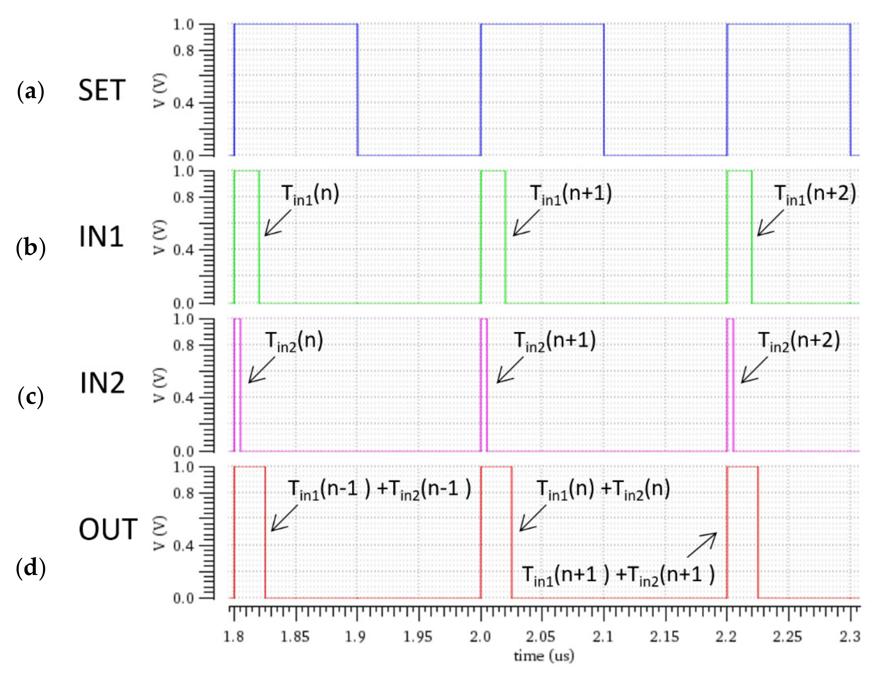
Figure 12 depicts the operation of a 2-input z−1 adder. The input pulse widths are 20 ns and 5 ns, respectively. The adder generates output pulses with pulse width Tout, which is the sum of the two preceding and equal to 25.08 ns. 
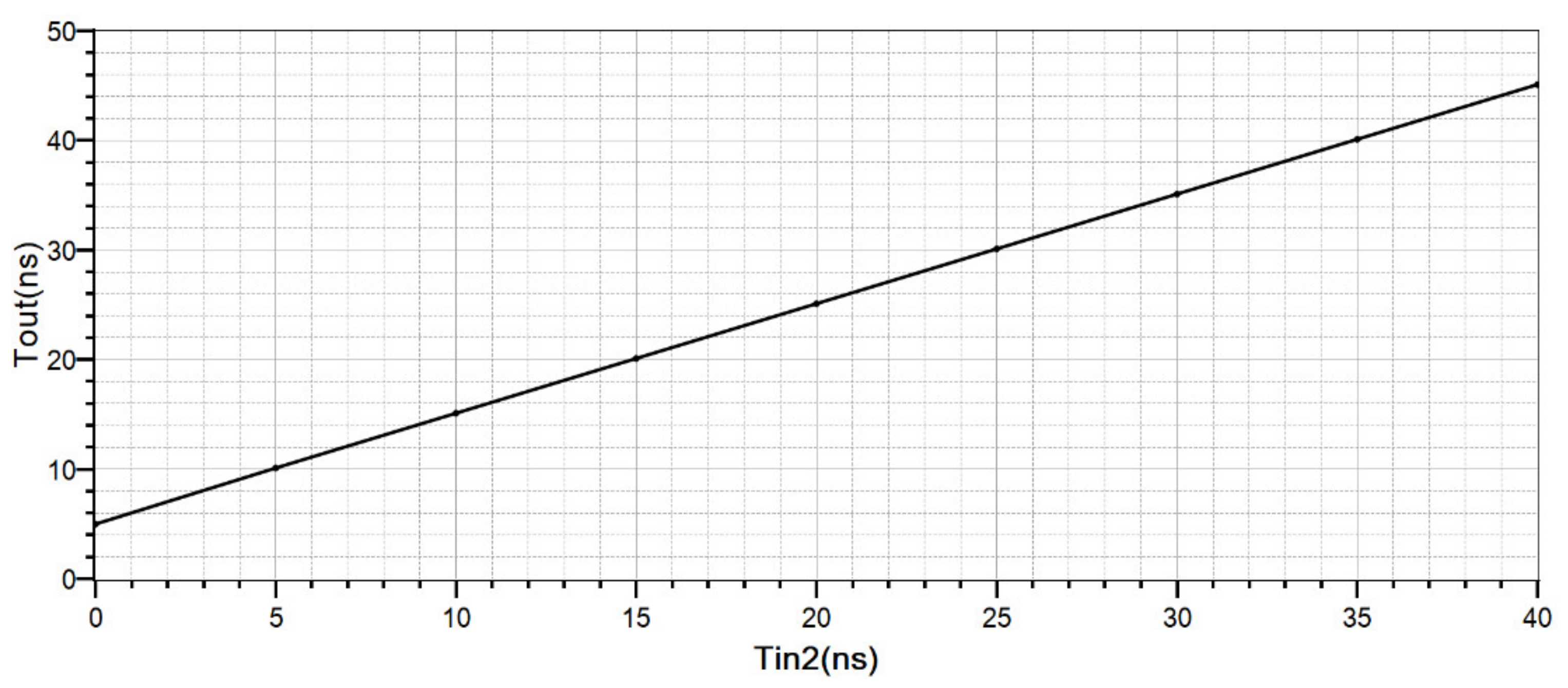
Figure 13 demonstrates the output pulse width of the Adder using a stable Tin1 at 5 ns at one input, while at the second input Tin2 ranges between 0 ns and 40 ns. It is obvious that the proposed adder can add linearly all values of the dynamic range of 40 ns.

6.3. Time-Mode FIR Filter

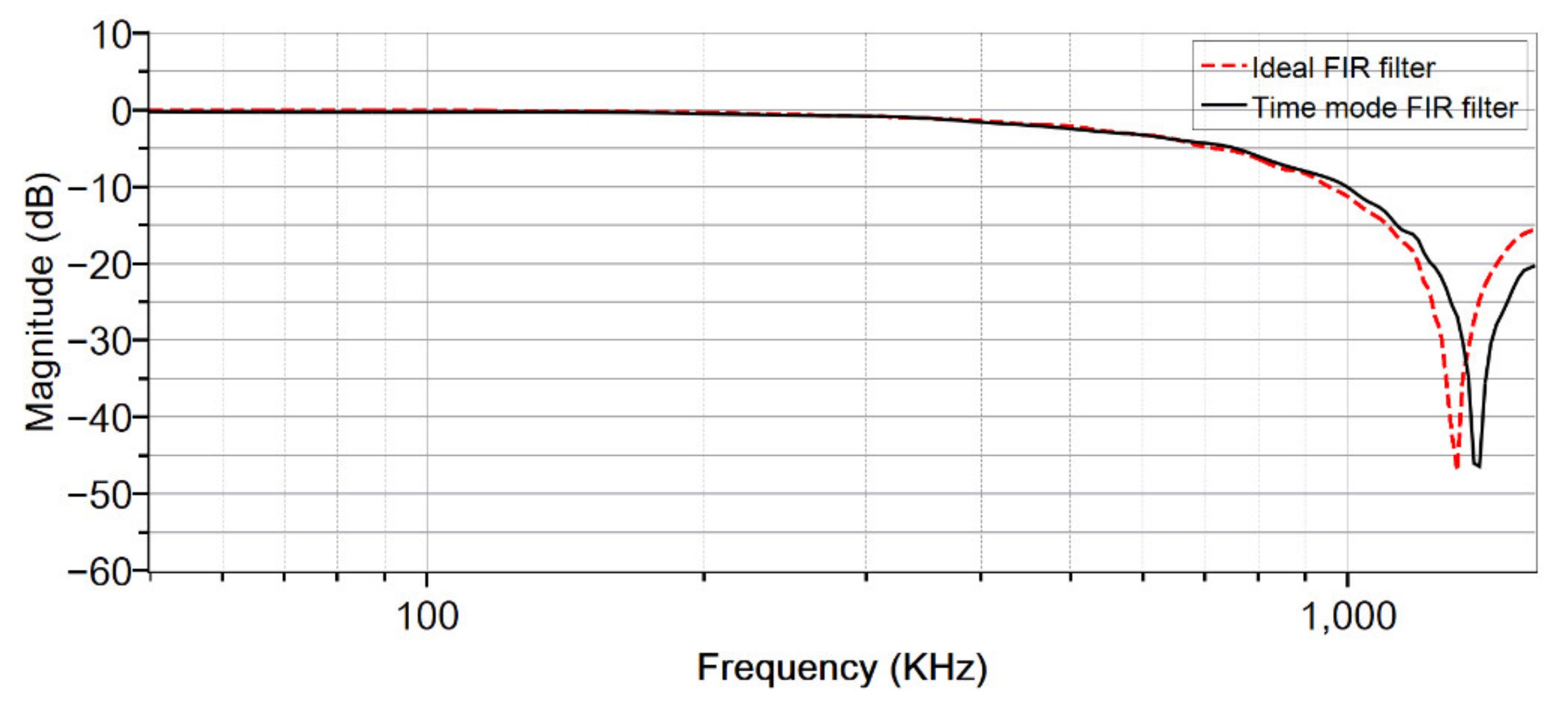
The simulated magnitude response of the ideal and the implemented time-mode 3rd-order FIR filter is presented in Figure 14. The sampling frequency was 5 MHz. The average power consumption is 200 μA, which includes the consumption of both actual filter circuit and digital calibration. The approximated filter coefficient values are presented in Table 1. The notch frequency of the ideal filter is selected to be around 1.31 MHz, which is close to the 1.38 MHz notch frequency of the implemented FIR filter. There is a frequency shift of 70 KHz. These frequency response discrepancies can be mainly attributed to the approximation error of the filter coefficients.
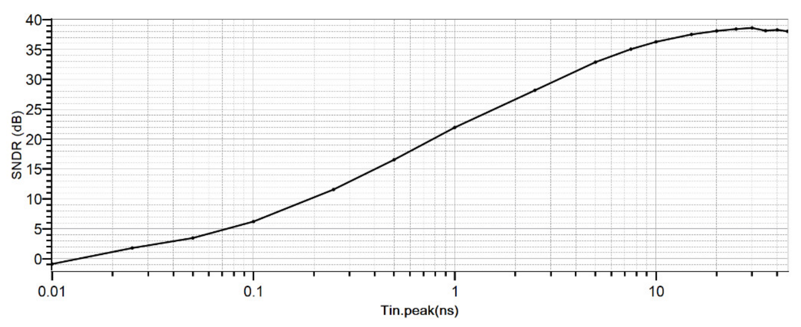
The SNDR simulated results versus Tin.peak are reported in Figure 15, where Tin.peak is the amplitude of a sinusoidal signal of 50 kHz. The SNDR peak is at around 38.6 dB.
The maximum input Tin is defined by the upper limit of the input signal of the z−1 structure, which is a bit less than 50 ns. The lower limit is mainly limited by the noise contribution of the MOS devices, which appeared as clock jitter, charge injection and leakage. Based on Figure 15, the noise level is around 10 ps.
Table 2 compares the proposed filter implementation to the state-of-the-art time-mode filters. Our implementation operates under the lowest power supply; it has relatively low power consumption for a 3rd order filter topology also using the highest sampling frequency.

7. Discussion

The proposed time-domain 3rd-order FIR rectangular filter is based on time-mode signal processing circuits such as the z−1 delay, z−1 multiplier and z−1 adder. The time register from [16] is used as a building component in all time-mode circuits in this work. The peak SNRR of the filter for a signal with frequency of 50 KHz is 38.6 dB. The average current consumption is 200 μA for a 5 MHz sampling frequency. This filter design offers numerous inherent advantages in time-mode signal processing. First, its outputs are synchronized with the sampling frequency. Second, because the topology is modular, filters of higher order may be created by simply increasing the number of delays and multipliers on the same complexity. Finally, the compatibility with the digital circuits makes it a perfect candidate for all-digital topologies that are widely used in state-of-the art topologies.
This technology can be utilized to produce other types of filters in the future, such as higher-order FIR or IIR filters. Time-mode controllers are also possible using this technique. The fabrication and the experimental verification of the proposed topology will be part of a future work.

Author Contributions

Conceptualization, O.P.-F. and S.V.; methodology, S.V.; validation, O.P.-F.; formal analysis, O.P.-F. and S.V.; investigation, O.P.-F. and S.V.; resources, S.V.; data curation, O.P.-F.; writing—original draft preparation, O.P.-F.; writing—review and editing, S.V.; visualization, O.P.-F. and S.V.; supervision, S.V.; project administration, S.V.; funding acquisition, O.P.-F. and S.V. All authors have read and agreed to the published version of the manuscript.

Funding

This research has been co-financed by the European regional development fund of the European union and Greek national funds through operational program competitiveness, entrepreneurship and innovation, under the call RESEARCH–CREATE–INNOVATE (project code: T1EDK-02551).

Conflicts of Interest

The authors declare no conflict of interest.

References

  1. Staszewski, R.; Muhammad, K.; Leipold, D.; Hung, C.-M.; Ho, Y.-C.; Wallberg, J.; Fernando, C.; Maggio, K.; Jung, T.; Koh, J.; et al. All-digital TX frequency synthesizer and discrete-time receiver for Bluetooth radio in 130-nm CMOS. IEEE J. Solid-State Circuits 2004, 39, 2278–2291. [Google Scholar] [CrossRef]
  2. Yuan, F. CMOS Time-Mode Circuits and Systems; CRC Press: Boca Raton, FL, USA, 2015. [Google Scholar]
  3. Asada, K.; Nakura, T.; Iizuka, T.; Ikeda, M. Time-domain approach for analog circuits in deep sub-micron LSI. IEICE Electron. Express 2018, 15, 20182001. [Google Scholar] [CrossRef] [Green Version]
  4. Park, Y.J.; Jarrett-Amor, D.; Yuan, F. Time integrator for mixed-mode signal processing. In Proceedings of the 2016 IEEE International Symposium on Circuits and Systems (ISCAS), Montreal, QC, Canada, 22–25 May 2016; pp. 826–829. [Google Scholar]
  5. Kim, N.; Kim, K.S.; Yu, W.; Cho, S.H. A Second-Order ΔΣ Time-to-Digital Converter Using Highly Digital Time-Domain Arithmetic Circuits. IEEE Trans. Circuits Syst. II Express Briefs 2019, 66, 1643–1647. [Google Scholar] [CrossRef]
  6. Leene, L.B.; Constandinou, T.G. Time Domain Processing Techniques Using Ring Oscillator-Based Filter Structures. IEEE Trans. Circuits Syst. I Regul. Pap. 2017, 64, 3003–3012. [Google Scholar] [CrossRef]
  7. Zhu, K.; Feng, J.; Lyu, Y.; He, A. High-precision differential time integrator based on time adder. Electron. Lett. 2018, 54, 1268–1270. [Google Scholar] [CrossRef]
  8. Karmakar, A.; De Smedt, V.; Leroux, P. Pseudo-Differential Time-Domain Integrator Using Charge-Based Time-Domain Circuits. In Proceedings of the 2021 IEEE 12th Latin America Symposium on Circuits and System (LASCAS), Arequipa, Peru, 21–24 February 2021; pp. 1–4. [Google Scholar] [CrossRef]
  9. Kwon, H.-J.; Lee, J.-S.; Sim, J.-Y.; Park, H.-J. A high-gain wide-input-range time amplifier with an open-loop architecture and a gain equal to current bias ratio. In Proceedings of the IEEE Asian Solid-State Circuits Conference 2011, Jeju, Korea, 14–16 November 2011; pp. 325–328. [Google Scholar] [CrossRef]
  10. Oulmane, M.; Roberts, G.W. CMOS Digital Time Amplifiers for High Resolution Timing Measurement. Analog Integr. Circuits Signal Process. 2005, 43, 269–280. [Google Scholar] [CrossRef]
  11. Li, Y.; Shepard, K.; Tsividis, Y. A Continuous-Time Programmable Digital FIR Filter. IEEE J. Solid-State Circuits 2006, 41, 2512–2520. [Google Scholar] [CrossRef] [Green Version]
  12. Ravinuthula, V.; Garg, V.; Harris, J.G.; Fortes, J.A.B. Time-mode circuits for analog computation. Int. J. Circuit Theory Appl. 2009, 37, 631–659. [Google Scholar] [CrossRef]
  13. Abdelfattah, M.; Roberts, G.W. All-Digital Time-Mode Direct-Form All-Pole Biquadratic Filter Realization. IEEE Trans. Circuits Syst. II Express Briefs 2017, 64, 1262–1266. [Google Scholar] [CrossRef]
  14. Guttman, M.M.; Roberts, G.W. Sampled-data IIR filtering using time-mode signal processing circuits. In Proceedings of the 2009 IEEE International Symposium on Circuits and Systems, Taipei, Taiwan, 24–27 May 2009; pp. 2285–2288. [Google Scholar]
  15. Orfeas, P.-F.; Vlassis, S. A novel time register with process and temperature calibration. In Proceedings of the 2021 10th International Conference on Modern Circuits and Systems Technologies (MOCAST), Thessaloniki, Greece, 5–7 July 2021; pp. 1–4. [Google Scholar]
  16. Panetas-Felouris, O.; Vlassis, S. A Time-Domain z−1 Circuit with Digital Calibration. J. Low Power Electron. Appl. 2022, 12, 3. [Google Scholar] [CrossRef]
  17. Sun, J. Pulse-Width Modulation. Pneum. Servo Syst. Anal. 2012, 2, 25–61. [Google Scholar]
  18. Finite Impulse Response (FIR) Filters. In Nonuniform Sampling; Springer: Berlin/Heidelberg, Germany, 2006; pp. 179–220.
Figure 1. Block diagram of the voltage-to-time conversion followed by a time-mode processing unit.
Electronics 11 00902 g001
Figure 2. Time-mode operators (a) z−1, (b) z−1 multiplier and (c) adder.
Electronics 11 00902 g002
Figure 3. (a) Time register circuit, (b) symbol and (c) timing diagram.
Electronics 11 00902 g003
Figure 4. (a) Time amplifier based on time register circuit and (b) symbol.
Electronics 11 00902 g004
Figure 5. (a) Time adder based on time register and (b) symbol.
Electronics 11 00902 g005
Figure 6. (a) Time-domain z−1 circuit, (b) clocks timing diagram and (c) pulses timing diagram.
Electronics 11 00902 g006
Figure 7. (a) Time-mode z−1 multiplier circuit, (b) pulses timing diagram.
Electronics 11 00902 g007
Figure 8. (a) Example of two inputs time-mode z−1 adder and a (b) pulses timing diagram.
Electronics 11 00902 g008
Figure 9. Implementation of 3rd order FIR filter with time-mode processing units.
Electronics 11 00902 g009
Figure 10. Timing waveforms for the z−1 multiplier for a multiplication coefficient equal to 0.28, (a) synchronization clock, (b) input pulses width with Tin = 20 ns and (c) output pulses with pulse width Tout = 5.55 ns.
Electronics 11 00902 g010
Figure 11. Two cases of multiplication coefficients with nominal values of 0.28 and 0.21 in relation to input pulse width Tin.
Electronics 11 00902 g011
Figure 12. Timing waveforms for a 2-input z−1 adder, (a) synchronization clock, (b) first input pulses with pulse width Tin1 = 20 ns, (c) second input pulses with pulse width Tin2 = 5 ns and (d) output pulses with pulse width Tout = 25.08 ns.
Electronics 11 00902 g012
Figure 13. Input-output of a 2-input adder for a constant Tin1 = 5 ns, while Tin2 ranges between 0 and 40 ns.
Electronics 11 00902 g013
Figure 14. Ideal and time-mode FIR frequency response.
Electronics 11 00902 g014
Figure 15. SNDR as function of Tin.peak for 50 KHz.
Electronics 11 00902 g015
Table 1. FIR filter coefficient values.
CoefficientExact
Value
Approximate
Value
Realization
α 1 × α 2
b00.23300.210.3 × 0.7
b10.26690.280.4 × 0.7
b20.26690.280.4 × 0.7
b30.23300.210.3 × 0.7
Table 2. Performance comparison with the state-of-the-art time-mode low-pass filters.
This Work[13][14][12]
Technology28 nm130 nm180 nm180 nm
Supply Voltage1 V1.2 V1.8 V5 V
Sampling Frequency5 MHz130 kHz5 MHz100 kHz
Filter Order3rd2nd2nd3rd
TypeFIR rectangularButterworthChebyshevIIR ChebyshevFIR
Peak SNDR38.6 dB47 dB37 dB44.1 dB-
Peak SNR---63.6 dB64 dB
Power Cons.200 μW152 μW187 μW760 μW89.45 μW
Publisher’s Note: MDPI stays neutral with regard to jurisdictional claims in published maps and institutional affiliations.

