Article

A New Fully Closed-Loop, High-Precision, Class-AB CCII for Differential Capacitive Sensor Interfaces

by
Gianluca Barile
1,
Francesco Centurelli
2,
Giuseppe Ferri
1,*,
Pietro Monsurrò
2,
Leonardo Pantoli
1,
Vincenzo Stornelli
1,
Pasquale Tommasino
2 and
Alessandro Trifiletti
2
1
Department of Industrial and Information Engineering and Economics, University of L’Aquila, 67100 L’Aquila, Italy
2
Department of Information, Electronics and Telecommunications Engineering, Sapienza University, 00184 Roma, Italy
*
Author to whom correspondence should be addressed.
Electronics 2022, 11(6), 903; https://doi.org/10.3390/electronics11060903
Submission received: 10 February 2022 / Revised: 11 March 2022 / Accepted: 14 March 2022 / Published: 15 March 2022
(This article belongs to the Special Issue Feature Papers in Circuit and Signal Processing)

Abstract

:
The use of capacitive sensors has advantages in different industrial applications due to their low cost and low-temperature dependence. In this sense, the current-mode approach by means of second-generation current conveyors (CCIIs) allows for improvements in key features, such as sensitivity and resolution. In this paper, a novel architecture of CCII for differential capacitive sensor interfaces is presented. The proposed topology shows a closed-loop configuration for both the voltage and the current buffer, thus leading to better interface impedances at terminals X and Z. Moreover, a low power consumption of 600 µW was obtained due to class-AB biasing of both buffers, and the inherent drawbacks in terms of linearity under the mismatch of class-AB buffering are overcome by its closed-loop configuration. The advantages of the novel architecture are demonstrated by circuit analysis and simulations; in particular, very good robustness under process, supply voltage and temperature variations and mismatches were obtained due to the closed-loop approach. The CCII was also used to design a capacitive sensor interface in integrated CMOS technology, where it was possible to achieve a sensitivity of 2.34 nA/fF, with a full-scale sensor variation of 8 pF and a minimum detectable capacitance difference of 40 fF.

1. Introduction

Nowadays, capacitive sensors can be considered a leading technology since they show inherent benefits for different kinds of measurements [1,2]. They are extremely versatile and can be realized in different ways, allowing their use in many applications [3,4,5,6,7]. In fact, capacitance variation can be obtained either by changing the capacitor geometry acting on the surface of the plates, or by shifting them, changing the overlapping area, or modifying the plates’ distance. Another solution may rely on the modification of the permittivity of the considered dielectric material, and this, for instance, also allows chemical changes in material compositions or physical parameters to be sensed [8].
Further advantages are the integration capability, the low-temperature dependance and the low cost, which make these kinds of sensors suitable for different industrial applications and uses. They can be employed, for instance, as accelerometers [9,10], pressure or moisture sensors [11,12], movement sensors [13] and concentration sensors [14]. Furthermore, no particular constraints can be found on sensor dimensions since, in principle, custom geometries and structures can be used for each application. However, miniaturization is a straightforward alternative, especially in many modern systems, in the form of integrated on-chip solutions. Moreover, capacitance variation, and so the dynamics of the sensor, can be easily defined and managed for the considered applications without particular criticism.
Among capacitive sensors, it is important to consider the differential ones, which are of particular interest since they show improved performance when used for the detection of low capacitance variations or in critical systems with interferences, providing even more robust sensing [15,16,17,18].
It is evident that, in this context, a critical role is played by the sensor interface, which should be easily integrated with the capacitive sensor and should be able to exploit sensor performance [19,20,21,22,23,24,25,26,27,28]. Different solutions have been provided in the literature, especially in recent years. Two main categories can be defined among capacitive sensor interfaces: the first one is represented by standard interfaces, without any compensation, which simply transduce the sensing parameter [19,20,21,25,26,28], while the second one collects interfaces that are able to compensate for parasitics by reducing the measurement error [22,23,24,27]. Moreover, an additional classification can be defined by considering the design approach, and, in particular, we can take into account both current-mode (CM) [23,25,27,28] and voltage-mode (VM) solutions [19,20,21,22,24,26,29].
One of the main drawbacks when considering a VM approach is that, especially in highly integrated low-pitch technologies, it is difficult to achieve good sensitivity, resolution and signal-to-noise ratios due to the narrow supply voltage rail, hence the intrinsically reduced voltage swing per variation that is to be measured. However, the current-mode approach could easily overcome this limitation; therefore, it represents an increasingly attractive methodology. One of the most famous CM active building blocks (ABBs) is the second-generation current conveyor (CCII), which inherits and expands the functionalities of its predecessor, the first-generation current conveyor (CCI) [30,31,32,33,34,35,36,37,38,39].
In this paper, we propose a completely novel architecture that implements a CCII especially designed for sensor interfacing applications. Favorably, the ABB uses a double IC-level feedback path, both for the voltage and the current subsections of the CCII, which allows for an improvement in the performance of the current buffer section and its robustness to process, supply voltage and temperature (PVT) variations and mismatches. In particular, the closed-loop configuration desensitizes circuit behavior from variations in component parameters, allowing stable performance under the variations, and mitigates the inherent drawbacks in terms of the linearity of the class-AB current buffer, allowing both low power and good linearity even under device mismatches. The proposed CCII was tested in a differential capacitive sensor exploiting the CM approach, and a sensitivity of 2.34 nA/fF with a full-scale sensor variation of 8 pF was achieved.
This manuscript is structured as follows: Section 2 introduces the proposed topology and shows its high-level working principle. Section 3 shows the IC-level in-depth analysis of the circuit, offering specific considerations for the differential capacitive sensor application. Section 4 presents the main simulation results and a comparison with the literature. In Section 5, conclusions are drawn.

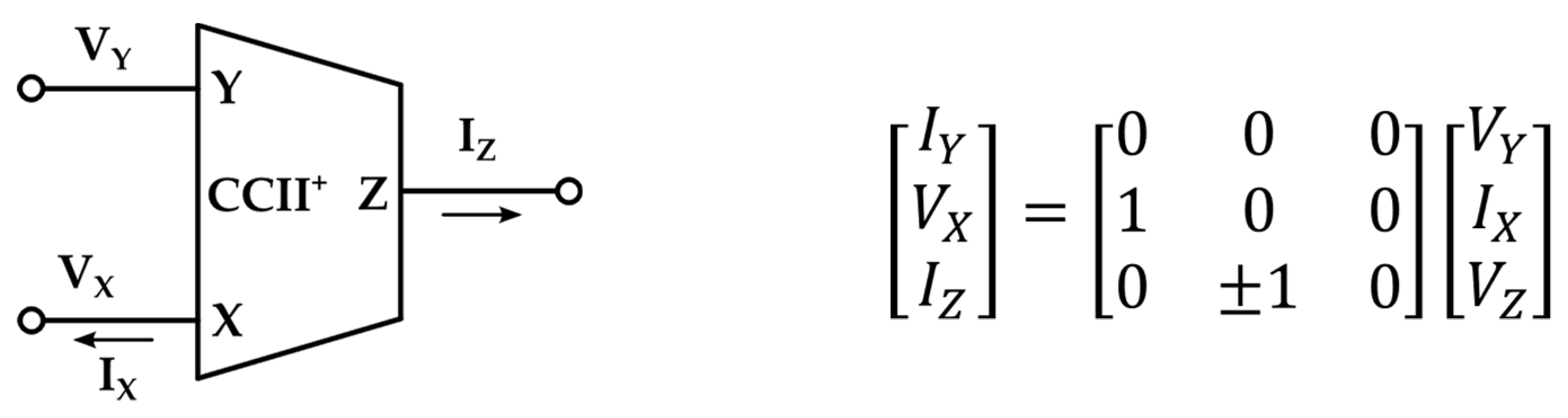
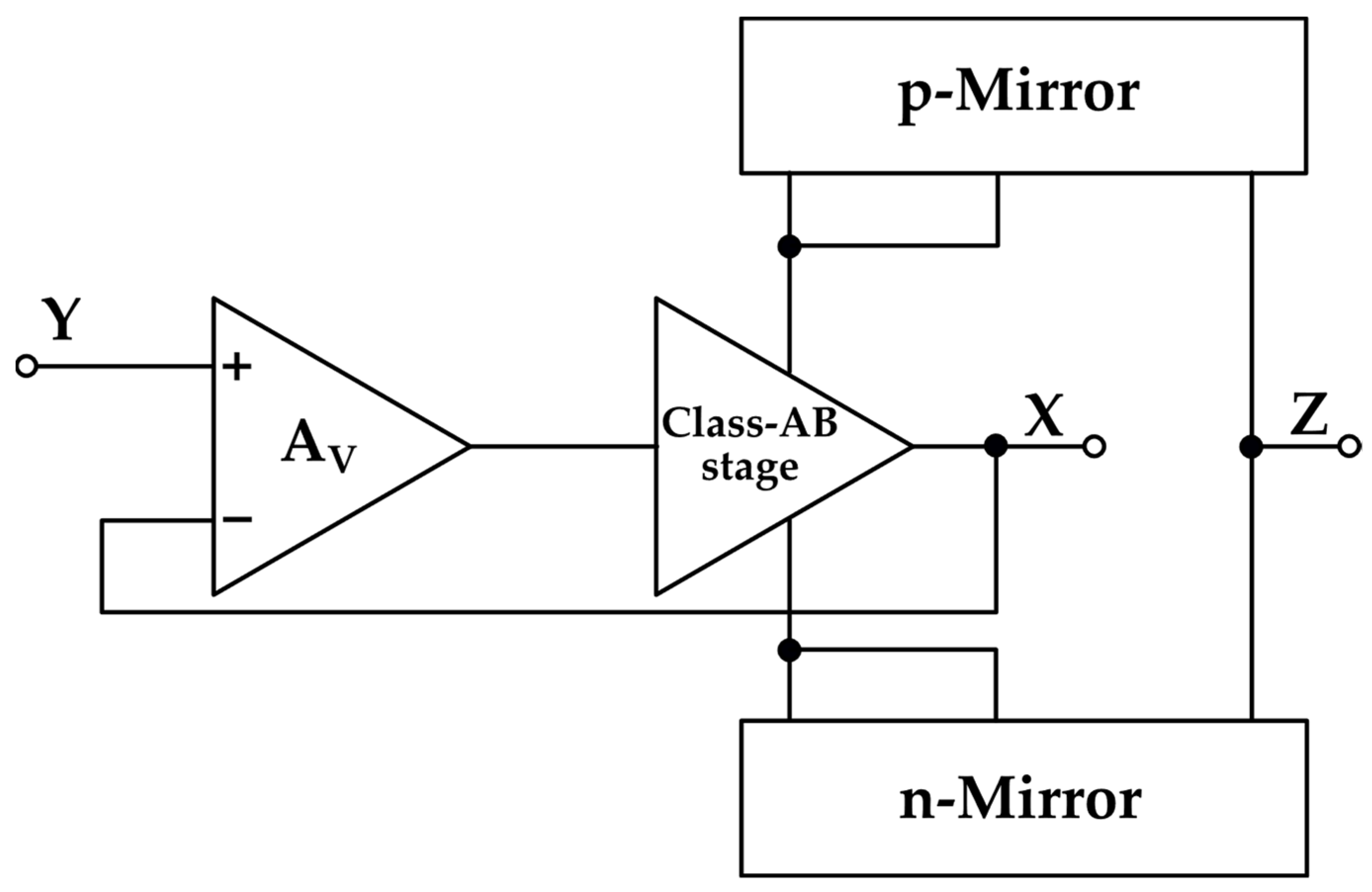
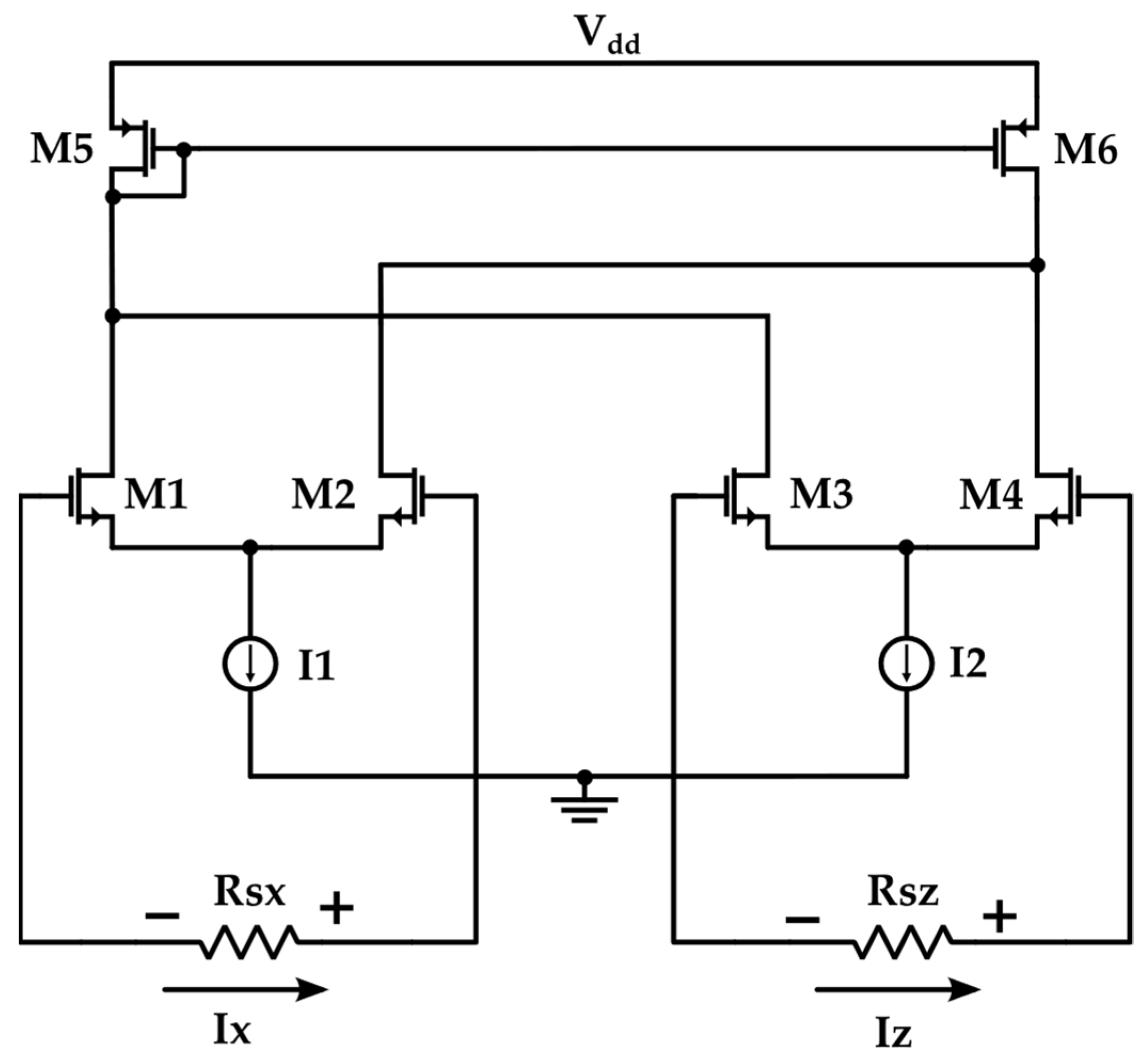
2. The Proposed Topology

The CCII is a three-port network, as shown in Figure 1, and in the ideal case, it is characterized by the equations VX = α VY, with α = 1, and Iz = β Ix, with β = 1; i.e., it is ideally composed of a voltage buffer between terminals Y and X and a current buffer between terminals X and Z. Closed-loop architectures are usually employed for the former, resulting in an accurate voltage gain α, wide bandwidth and low distortion, whereas a current mirror is typically employed for the current buffer since it naturally provides a wide bandwidth [30]. This, however, results in gain error on the current gain β, especially in low-voltage designs with deep submicron devices that present a low-output resistance, and in some nonlinearity in the current buffering action.
To deal with this problem, we implemented the proposed CCII topology, which exploits closed-loop architectures for both the voltage buffer and the current buffer, improving gain precision even under PVT variations. Moreover, the linearizing effect of the feedback allows class-AB topologies to also be used for the current buffer, resulting in a fully class-AB CCII topology, which can be useful in low-power applications.
The proposed CCII topology is shown in Figure 2 for the case of a non-inverting CCII (CCII+). The inverting topology (CCII) only requires the way in which R S X is connected to the left differential difference amplifier (DDA) inputs to be inverted. We provide a detailed analysis of this topology in Section 3, while in this section, we provide insights into its operation.
The voltage transfer function from node Y to node X must have an ideal unitary voltage gain, and this is ensured by voltage feedback, which also provides a high impedance at node Y and a low impedance at node X, thus amplifying the input error voltage V Y V X of the operational amplifier ( A V ), which drives a class-AB output stage with low-output impedance. Hence, the system inherently has high-input impedance and low-output impedance, while voltage feedback additionally improves both impedances. Furthermore, the output class-AB stage allows high power efficiency by providing large output currents at node X with a limited quiescent current. Linearity in the voltage transfer function is finally improved by feedback. The open-loop gain of the stage mostly depends on the operational amplifier A V . The input common-mode signal swing of the operational amplifier and the output signal swing of the output stage set the maximum and minimum voltages at nodes X and Y, respectively, as V X = V Y when the system operates correctly. Hence, large voltage swing operation is possible if the output stage and operational amplifiers are suitably designed, whereas the output current is limited by the (class-AB) output stage so that low-impedance high-current loads at node X can also be efficiently driven.
The operation of the voltage transfer function is straightforward, as its topology, composed of an operational amplifier and a class-AB output stage, is conventional. The only difference is the presence of the resistor R S X , which has some impact on the open-loop frequency response of the stage (as shown in Section 3). This resistor is necessary to sense the current flowing at node X and, thus, to obtain R S X = R S Z , the unity-gain current transfer function between nodes X and Z. The current transfer function is achieved by a novel class-AB architecture, which ensures high linearity and improved input and output impedances due to feedback. This is unlike conventional class-AB CCIIs, where a P-type current source, in parallel with an N-type current source, mirrors the push and pull currents at node X toward the output node Z, with an output impedance dependent on the topology of the current mirror (which is usually cascoded, if not gain-boosted, to maximize the output impedance).
The conventional approach (shown in Figure 3) to class-AB current buffering has a significant disadvantage in terms of linearity under mismatch variations. In fact, let us assume that the P-type current mirror has current gain A I P 1 and that the N-type current mirror has current gain A I N 1 . When both gains are unitary, no problem occurs; when a current enters node X, the P-type current mirror provides less current, and the N-type provides more current. In ideal class-AB operation, the positive (inflowing) current at node X would be mirrored to node Z by the N-type mirror, and the negative (outflowing) current would be mirrored by the P-type mirror. Both the N-type and P-type mirrors would amplify the input current by A I P = A I N = 1 in the ideal case. However, especially under mismatch variations, both A I P and A I N will not be unitary, and, above all, they will change differently, because mismatches among P devices will be mostly uncorrelated to mismatches among N devices. Hence, linearity will be greatly reduced under mismatches, because the positive output current will be amplified by a factor other than the negative output current. In an ideal class-AB current mirror, where the positive and negative parts of the signal are separately amplified by the N-type and P-type current mirrors, we have the following: I Z = I Z P + I Z N = A I P I X P + A I N I X N = A I P ( I X + | I X | ) 2 + A I N ( I X | I X | ) 2 = A I P + A I N 2 I X + A I P A I N 2 | I X | . Of course, the term A I P A I N 2 | I X | is heavily nonlinear and will be significant if large mismatches occur.
Because of this problem, in this work, we propose the closed-loop class-AB current mirror shown in Figure 2. The input current I X is sensed by the resistor R S X , so the left input of the DDA is fed by the input differential voltage R S X I X . However, the output current I Z is sensed by the resistor R S Z , so the right input of the DDA sees the differential input voltage R S Z I Z . The feedback loop provided by the DDA and the class-AB output stage copies the current at node X to node Z by enforcing R S Z I Z R S X I X . It also provides high output impedance at node Z, as the current at node Z is set by the current at node X, and, thus, node Z must have large impedance, as the current is insensitive to voltage variations. In order to prove this point, we consider Figure 4, where ideal current generators and current mirrors are assumed, so the equilibrium can only be reached when the currents of the output node are matched. Calling IDi, i = 1, 2, 3, 4, the drain currents of the four NMOS devices of the differential pairs, counted from left to right, we have
I D 1 = I B + g m R S X I X 2 ,   I D 2 = I B g m R S X I X 2
I D 3 = I B + g m R S Z I Z 2 ,     I D 4 = I B g m R S Z I Z 2 .
The equilibrium at the output node is given by
I D 1 + I D 3 = I D 2 + I D 4 2 I B + g m R S X I X + g m R S Z I Z 2 = 2 I B g m R S X I X + g m R S Z I Z 2
Hence, in this ideal case,
g m R S X I X + g m R S Z I Z = 0 I Z = R S X R S Z I X = I X .
under the hypothesis of R S X = R S Z = R s e n s e .
The class-AB output stage ensures that a large output current can be provided at node Z. However, when the input current at node X is large, the input differential voltages at the two inputs of the DDA become large, as they are R S X I X R S Z I Z , so it may happen that the DDA saturates with large input differential voltages. In order to avoid deep saturation, the maximum voltage across R S X = R S Z must not be much larger than the linear range of the inputs of the DDA. Thus, the value of the sensing resistors must be set by taking into account the maximum currents at terminals X and Z. However, a linear voltage-to-current transfer function in the DDA is not required for linearity to the extent that the DDA ensures that R S Z I Z is close to R S X I X ; however, when close to saturation, the two differential pairs of the DDA will show a limited gain, thus reducing the effectiveness of the feedback loop in ensuring good linearity.
The values of the sensing resistors RSX and RSZ have to be chosen by carefully weighing the trade-off among the maximum current, terminal impedances and noise, as shown by the simulations in Section 4.

3. Circuit Analysis

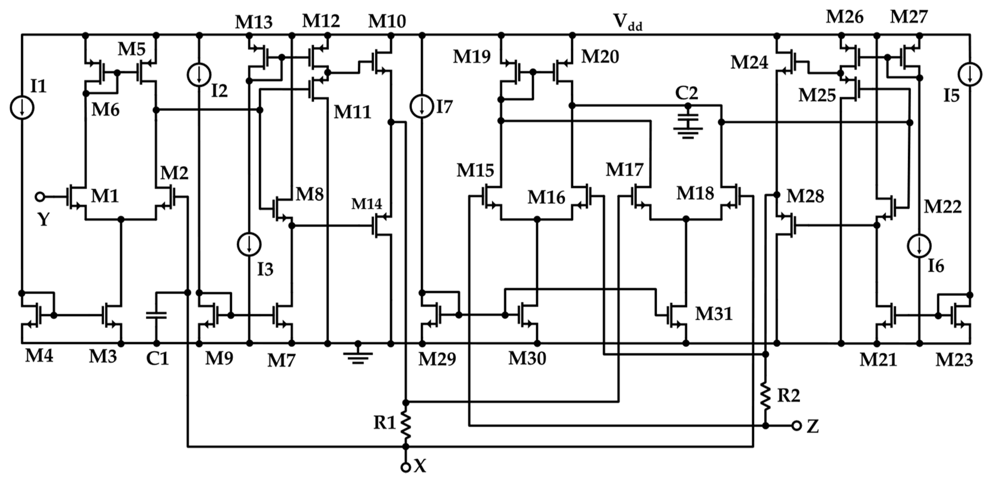
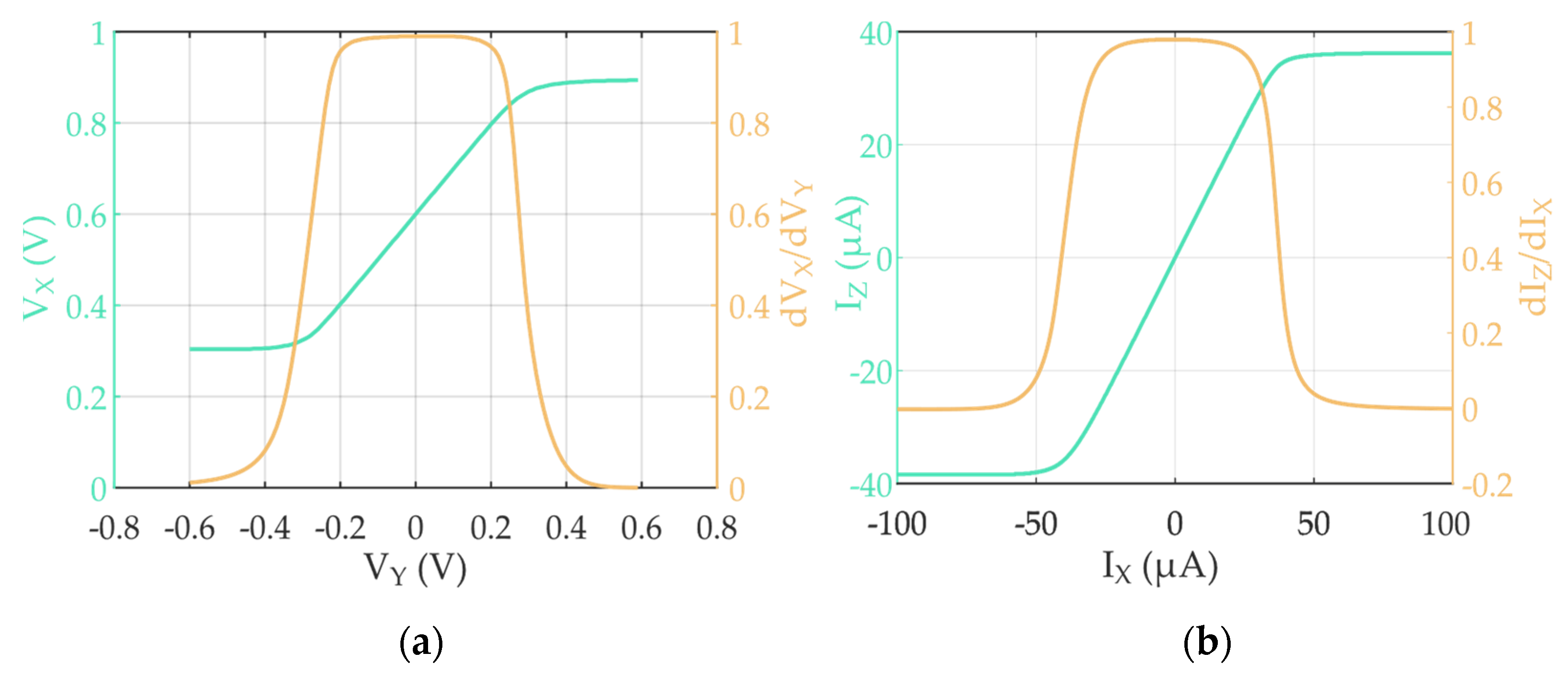
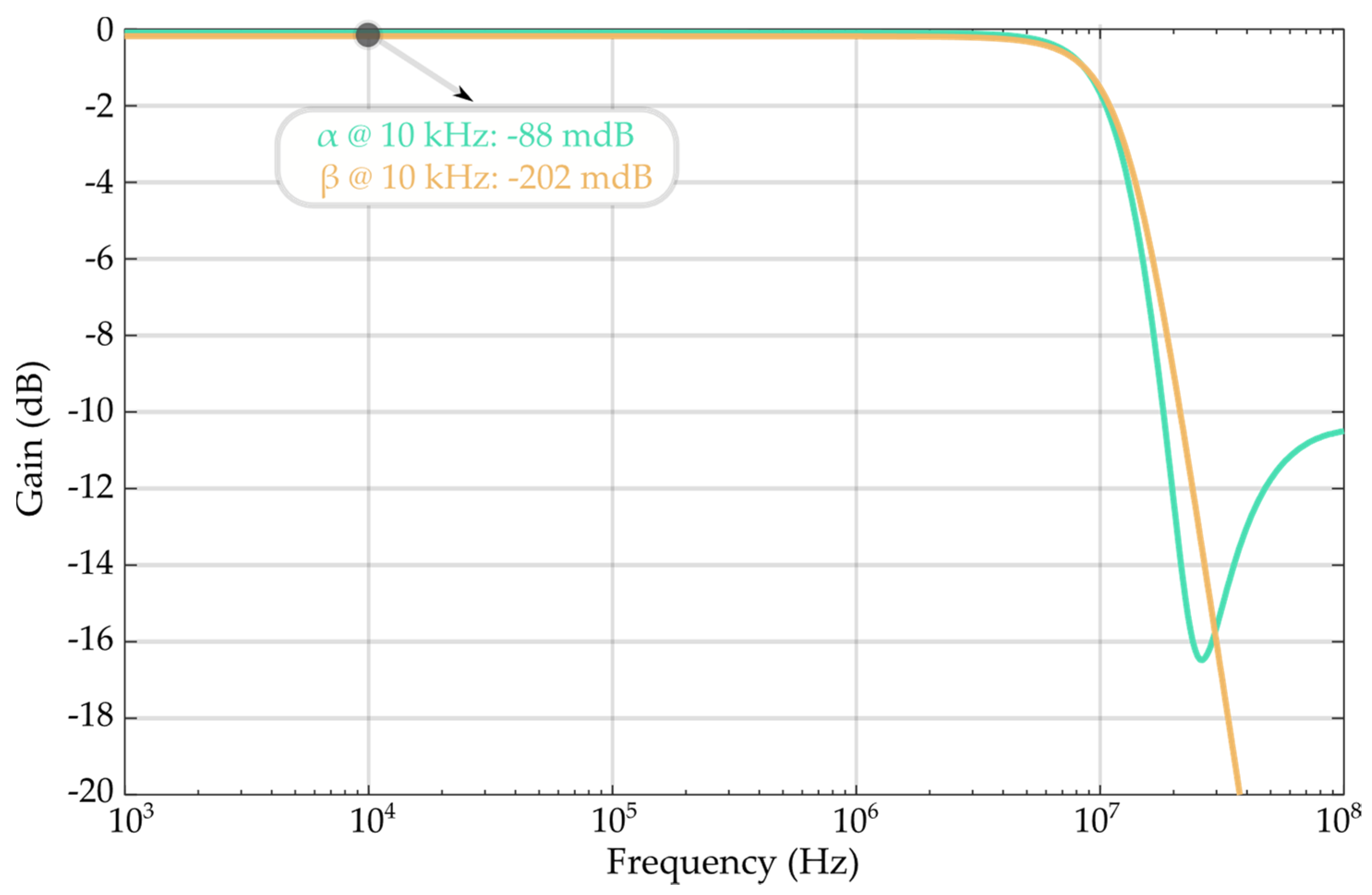
3.1. Analysis of the Proposed CCII

The proposed architecture of the current conveyor shown in Figure 2 has to be designed, at transistor level, by considering the ideal properties of a current conveyor; the negative feedback from both the Z and X outputs allows voltage gain α and current gain β to be obtained close to 1. If the same class-AB stage, showing voltage gain AVbuf and output resistance 1/gm, is used to design both the voltage buffer AI and the transconductance stage Gm in Figure 2, the following expressions for α and β are found:
α = A V · A V b u f 1 + A V · A V b u f ,
β = ± A D D A · A V b u f · g m R s e n s e 1 + g m R s e n s e 1 + A D D A · A V b u f · g m R s e n s e 1 + g m R s e n s e .
As can be seen from Equation (6), a sufficiently high value for Rsense has to be chosen in order not to degrade the gain of the current feedback loop too much.
At the same time, the feedback allows us to lower the impedance at the X node (RX) and to enhance the one at the Z node (RZ), as required, so that a very high RZ/RX ratio can be obtained:
R X = R s e n s e + 1 / g m 1 + A V · A V b u f ,
R Z = ( R s e n s e + 1 / g m ) · ( 1 + A D D A · A V b u f · g m R s e n s e 1 + g m R s e n s e ) ,
R Z R X = ( 1 + A V · A V b u f ) · ( 1 + A D D A · A V b u f · g m R s e n s e 1 + g m R s e n s e ) .
The presence of the Rsense resistor allows the open-loop impedance at node Z to be enhanced, but, unfortunately, it also increases the open-loop impedance at node X; if a given closed-loop RX is specified, the gain of the voltage feedback loop and the value of Rsense have to be jointly designed in order obtain the required RX value according to Equation (7). Then, the gain of both feedback loops (in terms of AV, ADDA, AVbuf and 1/gm) must be designed to be sufficiently high and, at the same time, to permit the desired RZ/RX ratio (>1000 in most practical cases). It has to be noted that the value of Rsense also affects the noise and linear range of the CCII, as shown in the simulation Section, thus making the choice of the most appropriate value even more critical.

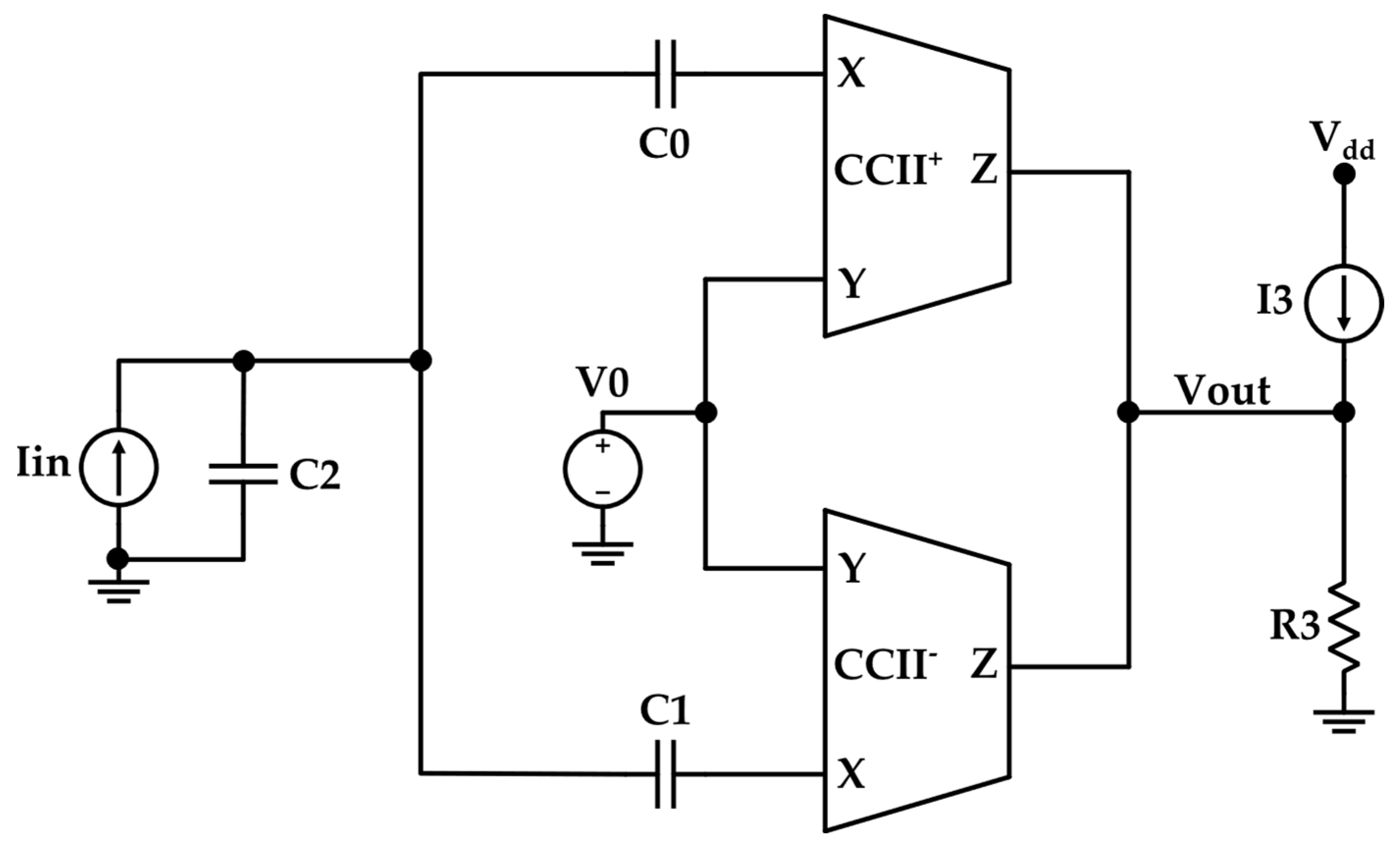
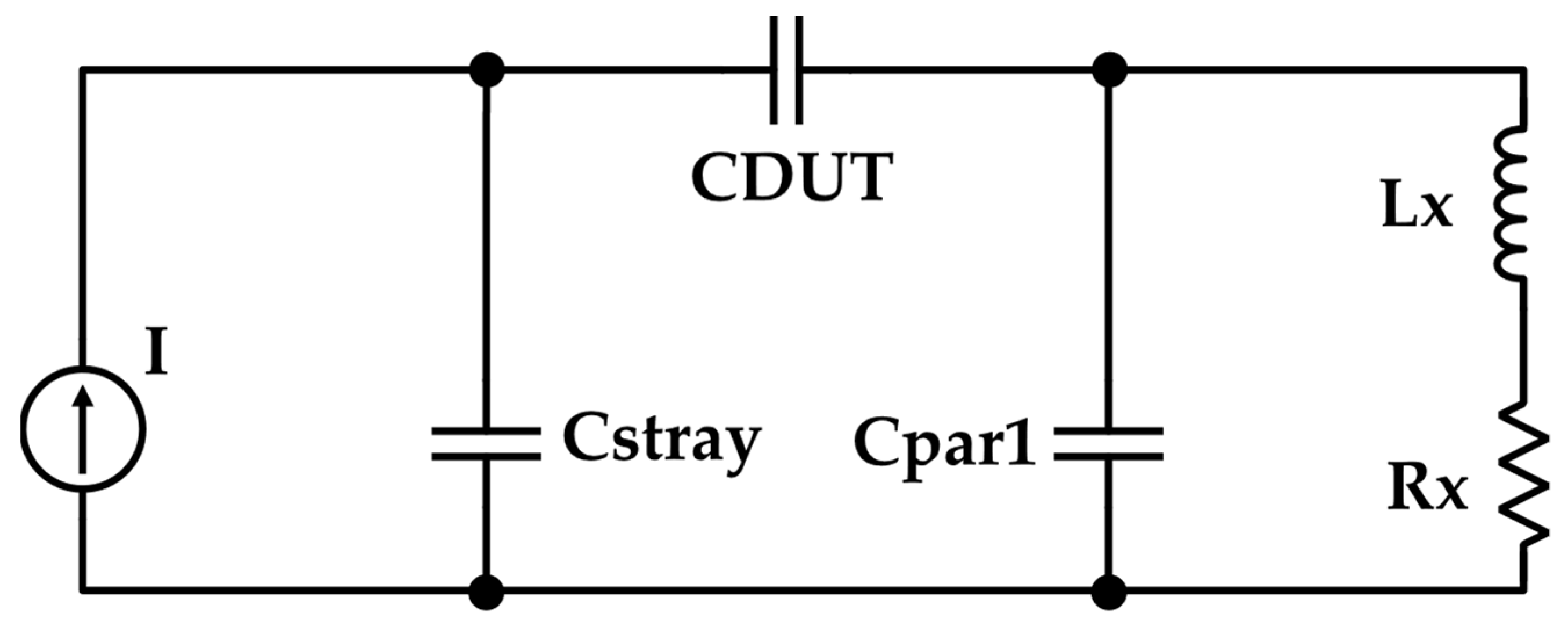
3.2. Application as Differential Capacitive Sensor Interface

The proposed CCII can be applied in a differential capacitive sensor, whose architecture is shown in Figure 5. Two CCIIs, one inverting and the other non-inverting, were employed to sense the differential current passing through two capacitors, namely, C0 and C1, whose difference has to be measured. An input current generator provides a square wave with period T and amplitude IREF, which is fed to the two capacitors (C2 in Figure 6 represents parasitic capacitance at the input node). The input node voltage increases and decreases linearly with slope Iin/(C0 + C1 + C2); thus, there is a trade-off between the input current amplitude, the square wave period—related to the speed of the variation in the capacitance difference—and the average value of the capacitances C0 and C1 due to there being a limit on the maximum value that the input voltage can assume. The CCIIs buffer the currents through the capacitors, and their output currents are summed on resistor R3, providing the output voltage Vout. The output voltage during the positive cycle of the square wave is thus dependent on the capacitance difference C1C0, provided that the circuit operates in the linear region. As an alternative, current-mode processing can be adopted, with the output current read by some current input block (e.g., a current amplifier or a transimpedance amplifier); in this case, I3 and R3 in Figure 5 model the input of such a block. Techniques to compensate for the stray capacitance C2 are discussed in [27] and are outside the scope of this paper.
The use of the proposed CCII scheme as a current-mode interface for capacitive sensors therefore also requires a more accurate analysis of parasitic capacitance at input node X. It can be seen that a parasitic capacitance Cpar1 at node X is found, given by the sum of the parasitic capacitance at the AV- input and the parasitic capacitance at the negative ADDA input. Moreover, a parasitic capacitance Cpar2 (<Cpar1) is found at the positive ADDA input. The expression for the overall input impedance at node X, ZX, is the following:
Z X = 1 s C p a r 1   | |   Z X 1 s C p a r 1   | |   R X ,
where
Z X = R X · ( 1 + s · C p a r 2 R s e n s e 1 + g m R s e n s e ) = R X + s · L X R X ,
and
L X = C p a r 2 R s e n s e R X 1 + g m R s e n s e .
The parasitic capacitance Cpar2 creates a zero in the ZX′ expression, and an equivalent inductance can be considered to account for its frequency behavior; particular care has to be paid during the design of the CCII, so the zero of ZX′ is placed outside the range of the input frequencies used as a stimulus for the sensor interface. Under the previous hypothesis, the approximate expression in Equations (10) and (11) can be adopted.
In the general case, the model in Figure 6 has to be considered for the input terminal of the current-mode sensor interface. The stray capacitance CStray of the sensor (equivalent to half C2 in Figure 5) has to be estimated in order to calibrate the measurement and improve accuracy. The following partition function αSENS is found between the current stimulus I and the current IDUT entering the sensor:
α S E N S = C D U T C D U T + C S t r a y · 1 + s · C p a r 1 R X ( 1 + s · L X / R X ) 1 + s · ( C p a r 1 + C D U T C S t r a y C D U T + C S t r a y ) R X ( 1 + s · L X / R X ) .
A second condition, concerning the time constant τ 1 = L X / R X , has to be fulfilled in order to set the input bandwidth of the interface. Moreover, the time constant τ2, given by
τ 2 = R X · ( C p a r 1 + C D U T C S t r a y C D U T + C S t r a y )
has to be suitably chosen in order to avoid limits in the input bandwidth of the sensor interface.

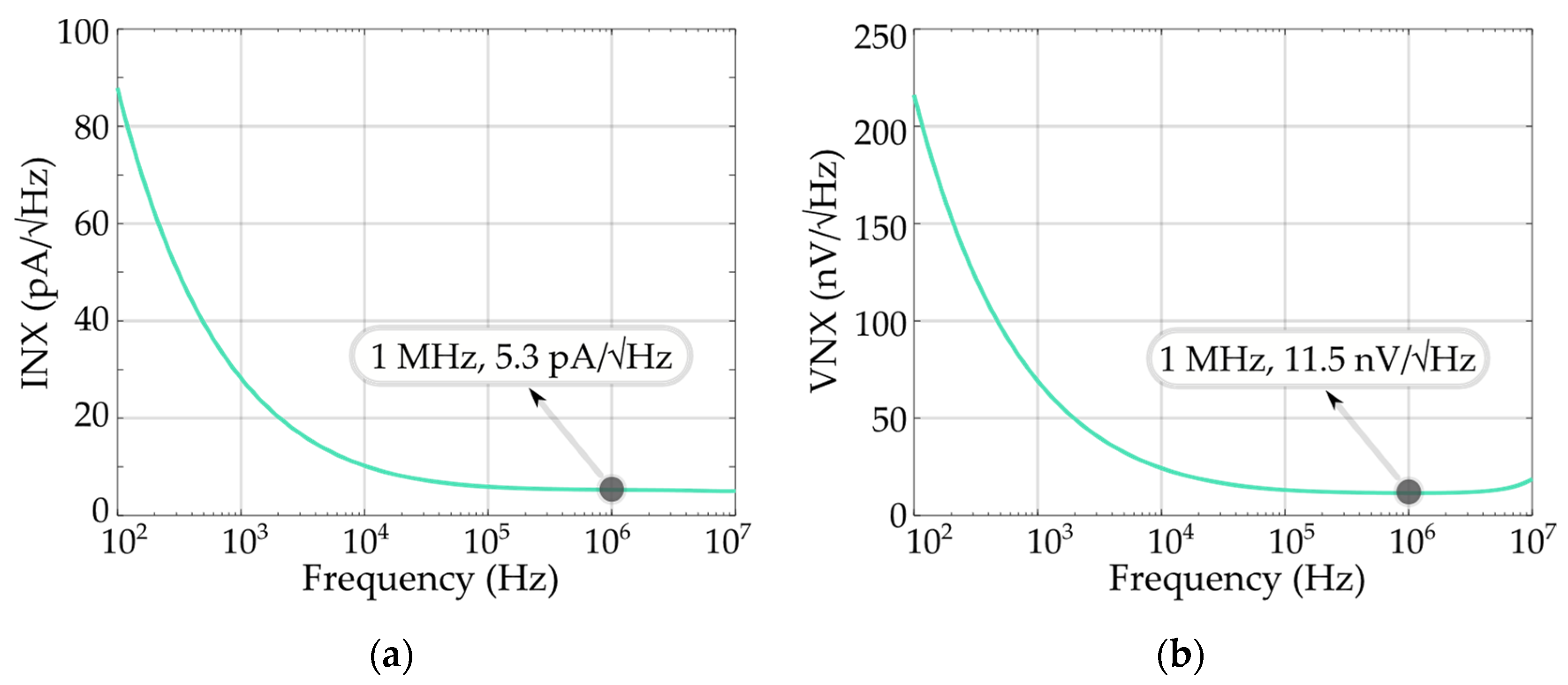
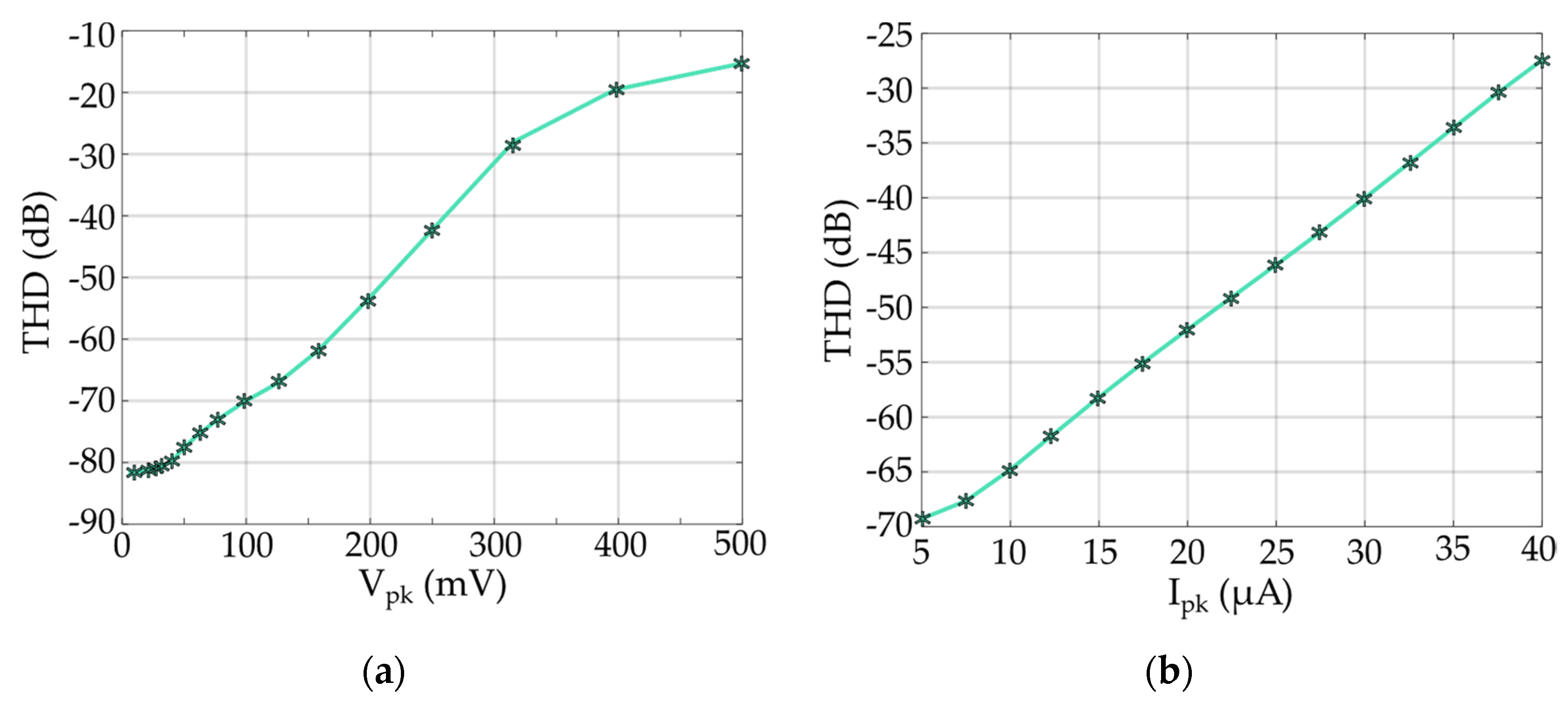
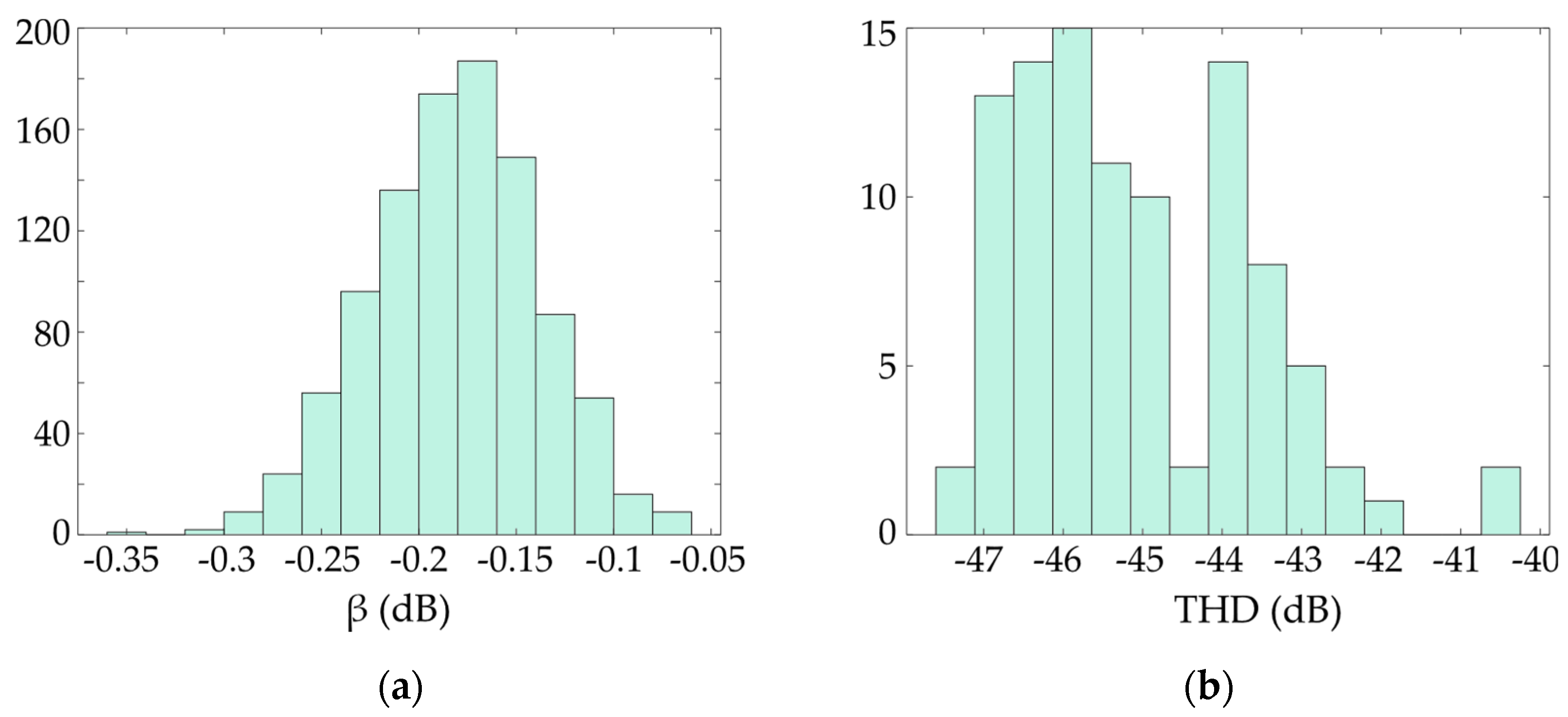
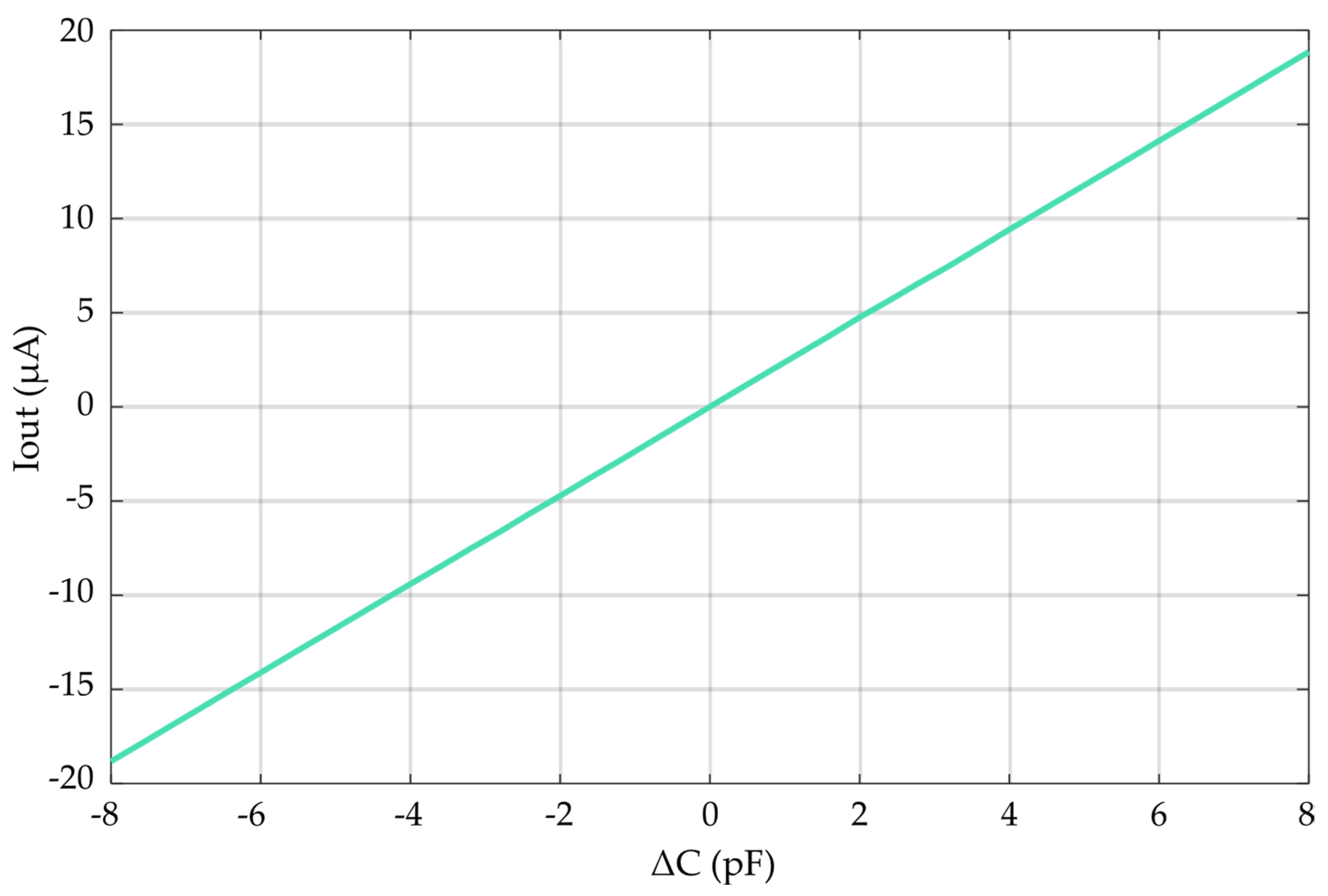
4. Simulation Results of a Sensor Design Case Study

Both inverting and non-inverting CCIIs based on the proposed approach were designed and simulated using the Cadence software suite, in a 130 nm CMOS technology from STMicroelectronics, in order to develop a current-based sensor interface for differential capacitance [25] based on the architecture described in Section 3.2 [28]. The two feedback loops were designed with an overall voltage gain of about 40 dB for the cascade of the block AV (or DDA) and buffer. In Figure 7, the transistor implementation of the CCII+ stage is shown. The current mirrors were designed to bias the AV stage with a 29.9 µA tail current (M3), the DDA stage with a 14.9 µA tail current (M30, M31) and the class-AB stages with 68.8 µA (M7, M21) and 39.7 µA (M13, M26) tail currents. The overall power consumption from a 1.2 V supply voltage is about 600 µW. The transistor sizes are reported in Table 1.
To evaluate the effect of the sensing resistor on CCII performance, simulations for two different values of Rsense are reported. When Rsense is set to 5 kΩ, the DC transfer functions shown in Figure 8 are achieved. The input range at terminal Y is about ±250 mV, and the current range is about ±30 μA, limited by the input voltage range of the DDA. The corresponding small-signal performance is reported in Figure 9, and it shows small gain errors with bandwidths of 12 MHz and 12.8 MHz for the voltage and current buffers, respectively. In particular, the value of Rsense allows a loop gain of 47.5 dB to be achieved, resulting in a closed-loop current gain of about −0.2 dB. Figure 10 reports the impedances at the terminals of the CCII, highlighting a ratio of impedances at Z and X terminals larger than 1000 and up to 100 kHz.
The modeling inductor LX defined in Section 3.2 is equal to 99.7 μH. Capacitive behavior can be seen at high frequencies for ZX; from the graph in Figure 10, the value CX = 0.9 pF is evaluated. Finally, analysis of the ZZ graph allows the definition of a modeling capacitance CZ = 3.5 pF.
In Figure 11, the input equivalent noise current at terminal X and the noise voltage at terminal Y are reported: an input equivalent noise voltage VNY = 11.5 nV/√Hz at terminal Y and an input equivalent noise current INX = 5.3 pA/√Hz at terminal X can be observed at 1 MHz.
Linearity was evaluated by testing both the voltage buffer and the current buffer with a 100 kHz sinusoidal input, and Figure 12 reports the total harmonic distortion (THD) versus the input amplitude. The relatively large value of Rsense leads to significant distortions of the current buffer for currents in the range of tenths of μA, with −40 dB THD achieved at 30 μA. From this point of view, this choice of sensing resistor seems appropriate when a relatively large load resistance at the X terminal is used.
The simulations were repeated in the case Rsense = 500 Ω, and the main performance parameters for both of the designs are reported in Table 2. Scaling the sense resistors obviously directly impacts the terminal impedances; in particular, a lower sense resistor results in a lower RX, which is an advantage in many applications, but also a lower RZ. The ratio of terminal resistances remains approximately constant. The loop gain of the feedback in the current buffer reduces to 31.5 dB, allowing a closed-loop gain β of about −0.27 dB.
A lower series resistance results in a wider linear range for the current buffer, as shown by the DC transfer curve in Figure 13a, but also in a higher equivalent noise current at terminal X (about 48.4 pA/√Hz at 1 MHz). The plot of THD versus peak input current for a 100 kHz sinusoidal input is reported in Figure 13b. The voltage buffer results were practically unaffected by the value of Rsense, apart from the value of the resistance at node X.
Analysis of the CCII+ performance under process, voltage supply and temperature (PVT) variations was carried out, together with a Monte Carlo analysis involving process variations and mismatches at 27 °C and nominal voltage supply. Table 3 and Table 4 report the results for the case of Rsense = 5 kΩ (similar results were obtained at 500 Ω). Table 3 shows a very low variation in the current gain under PVT variations: this good result is due to the use of a closed-loop approach for the current buffer, where feedback is employed to desensitize the performance from variations in the open-loop gain. Analogously, the Monte Carlo results reported in Table 4 show a very good stability of the gain and distortion. This is in contrast with the results typically achieved in class-AB CCIIs with an open-loop current buffer, where distortion under mismatch is much worse than that obtained in typical conditions [39]. Histograms for the current gain and the THD of the current buffer for a peak input current of 25 μA are reported in Figure 14 to better highlight the advantage of the proposed approach.
The proposed CCII was also used to simulate the differential capacitive sensor in Figure 5. Given the 3 dB bandwidth of the CCII, we chose a frequency of 2 MHz for the input square wave current. The peak value of such a current has to be determined according to the average value CDUT of the capacitances; for CDUT = 4 pF, limited by stability considerations, a peak current of 20 μA was chosen. The CCII was sized with sensing resistors Rsense = 500 Ω as a trade-off between speed, terminal impedances and noise.
Figure 15 reports the resulting characteristic of the sensor (output current in the positive period of the square wave vs. capacitance difference), which shows very good linearity for the whole range of variations in the capacitance (C0, C1 = CDUT ± ΔC/2, with CDUT = 4 pF) and allows a sensitivity of about 2.34 nA/fF to be estimated. Transient noise simulations allow us to estimate an output noise current of 94 nA rms, corresponding to a minimum detectable ΔC of 40 fF.
Table 5 reports the main performance parameters of the sensor and compares them with similar reports in the literature. To allow an easy comparison between different implementations, the following figure of merit is defined:
F O M = B W P d Δ C m a x Δ C m i n
where the bandwidth BW is calculated as half of the clock frequency and the minimum ΔC is obtained from noise and sensitivity values, if not explicitly declared in the papers. While the best FOM is achieved by the sensor in [27], which uses very simple circuits for the readout, the proposed sensor, which has not been optimized for noise, shows interesting results regardless, allowing a large bandwidth and a large CDUT at the same time.

5. Conclusions

A novel architecture of a second-generation current conveyor, which also exploits a closed-loop feedback approach for the current buffer, was presented, thus combining the advantages of class-AB biasing with the linearizing and desensitizing effects of feedback. In addition to good linearity, very robust performance was in fact achieved under PVT variations and device mismatches due to the use of a unity-gain feedback loop for the X-Z transfer. Inverting and non-inverting CCIIs can be easily obtained by simply changing the sign of the differential voltage, thus maximizing the symmetry in applications where both conveyors are needed and have to be matched. Sensing resistors were employed to implement the current feedback loop, and their values can be optimized according to the required application by finding the desired trade-off between gain precision, bandwidth, linearity and noise.
A CCII was designed in a 130 nm CMOS technology by STMicroelectronics, and it was characterized for different values of the sensing resistors to highlight the trade-offs. PVT and Monte Carlo simulations showed very good robustness of the performance for both the voltage and current buffers. An inverting and a non-inverting CCII were employed to design and simulate a differential capacitive sensor interface that allows a high operating frequency with large capacitive values and good linearity for a 100% variation in the capacitance.

Author Contributions

Conceptualization: P.M.; methodology: F.C., P.T., A.T.; software: P.T., G.B.; validation: F.C., P.M., G.F., V.S.; formal analysis: P.T.; investigation: F.C., P.M., P.T.; writing—original draft preparation: P.M., P.T., G.B., L.P.; writing—review and editing: F.C., G.F., L.P.; supervision: F.C., G.F., V.S. All authors have read and agreed to the published version of the manuscript.

Funding

This research received no external funding.

Conflicts of Interest

The authors declare no conflict of interests.

References

  1. Capacitive Sensors: Design and Applications; Wiley-IEEE Press: Hoboken, NJ, USA, 1997; Available online: https://ieeexplore.ieee.org/book/5264832 (accessed on 18 January 2022).
  2. Puers, R. Capacitive sensors: When and how to use them. Sens. Actuators A Phys. 1993, 37–38, 93–105. [Google Scholar] [CrossRef]
  3. Dong, T.; Gu, Y.; Liu, T.; Pecht, M. Resistive and capacitive strain sensors based on customized compliant electrode: Comparison and their wearable applications. Sens. Actuators A Phys. 2021, 326, 112720. [Google Scholar] [CrossRef]
  4. Qian, H.; Hrnjak, P. Characterization of R134a two-phase flow regimes in horizontal and vertical smooth tubes with capacitive sensors. Int. J. Refrig. 2021, 125, 90–103. [Google Scholar] [CrossRef]
  5. Wang, W.; Zhao, K.; Zhang, P.; Bao, J.; Xue, S. Application of three self-developed ECT sensors for monitoring the moisture content in sand and mortar. Constr. Build. Mater. 2021, 267, 121008. [Google Scholar] [CrossRef]
  6. Zeng, T.; Lu, Y.; Liu, Y.; Yang, H.; Bai, Y.; Hu, P.; Li, Z.; Zhang, Z.; Tan, J. A Capacitive Sensor for the Measurement of Departure From the Vertical Movement. IEEE Trans. Instrum. Meas. 2015, 65, 458–466. [Google Scholar] [CrossRef]
  7. Ferlito, U.; Grasso, A.; Vaiana, M.; Bruno, G. A Time-Based Electronic Front-End for a Capacitive Particle Matter Detector. Sensors 2021, 21, 1840. [Google Scholar] [CrossRef]
  8. Andrés, M.A.; Vijjapu, M.T.; Surya, S.G.; Shekhah, O.; Salama, K.N.; Serre, C.; Eddaoudi, M.; Roubeau, O.; Gascón, I. Methanol and Humidity Capacitive Sensors Based on Thin Films of MOF Nanoparticles. ACS Appl. Mater. Interfaces 2020, 12, 4155–4162. [Google Scholar] [CrossRef]
  9. Ramakrishnan, J.; Gaurav, P.T.R.; Chandar, N.S.; Sudharsan, N.M. Structural design, analysis and DOE of MEMS-based capacitive accelerometer for automotive airbag application. Microsyst. Technol. 2020, 27, 763–777. [Google Scholar] [CrossRef]
  10. Martínez, J.; Asiain, D.; Beltrán, J. Lightweight Thermal Compensation Technique for MEMS Capacitive Accelerometer Oriented to Quasi-Static Measurements. Sensors 2021, 21, 3117. [Google Scholar] [CrossRef]
  11. Li, R.; Zhou, Q.; Bi, Y.; Cao, S.; Xia, X.; Yang, A.; Li, S.; Xiao, X. Research progress of flexible capacitive pressure sensor for sensitivity enhancement approaches. Sens. Actuators A Phys. 2021, 321, 112425. [Google Scholar] [CrossRef]
  12. Okasha, A.; Ibrahim, H.; Elmetwalli, A.; Khedher, K.; Yaseen, Z.; Elsayed, S. Designing Low-Cost Capacitive-Based Soil Moisture Sensor and Smart Monitoring Unit Operated by Solar Cells for Greenhouse Irrigation Management. Sensors 2021, 21, 5387. [Google Scholar] [CrossRef] [PubMed]
  13. Shiah, J.; Rashtian, H.; Mirabbasi, S. A Low-Noise Parasitic-Insensitive Switched-Capacitor CMOS Interface Circuit for MEMS Capacitive Sensors. In Proceedings of the 2011 IEEE 9th International New Circuits and Systems Conference, Bordeaux, France, 26–29 June 2011; pp. 470–473. [Google Scholar]
  14. Litvinov, A.; Samotaev, N.; Etrekova, M.; Ivanova, A.; Filipchuk, D. Hydrogen Concentration Control in Oil-Filled Power Transformers Using Field Effect Capacitive Gas Sensors. J. Electrochem. Soc. 2021, 168, 017503. [Google Scholar] [CrossRef]
  15. Gupta, N.; Dutta, S.; Panchal, A.; Yadav, I.; Kumar, S.; Parmar, Y.; Vanjari, S.R.K.; Jain, K.K.; Bhattacharya, D.K. Design and Fabrication of SOI Technology Based MEMS Differential Capacitive Accelerometer Structure. J. Mater. Sci. 2019, 30, 15705–15714. Available online: https://www.springerprofessional.de/en/design-and-fabrication-of-soi-technology-based-mems-differential/17036044 (accessed on 13 March 2022). [CrossRef]
  16. Eswaran, P.; Malarvizhi, S. Design Analysis of MEMS Capacitive Differential Pressure Sensor for Aircraft Altimeter. Int. J. Appl. Phys. Math. 2012, 2, 14–20. [Google Scholar] [CrossRef] [Green Version]
  17. Li, R.; Mohammed, Z.; Rasras, M.; Elfadel, I.; Abe, M.; Choi, D. Design, modelling and characterization of comb drive MEMS gap-changeable differential capacitive accelerometer. Measurement 2021, 169, 108377. [Google Scholar] [CrossRef]
  18. Aydemir, A.; Terzioglu, Y.; Akin, T. A new design and a fabrication approach to realize a high performance three axes capacitive MEMS accelerometer. Sens. Actuators A Phys. 2016, 244, 324–333. [Google Scholar] [CrossRef]
  19. Depari, A.; Sisinni, E.; Flammini, A.; Ferri, G.; Stornelli, V.; Barile, G.; Parente, F.R. Autobalancing Analog Front End for Full-Range Differential Capacitive Sensing. IEEE Trans. Instrum. Meas. 2018, 67, 885–893. [Google Scholar] [CrossRef]
  20. Barile, G.; Ferri, G.; Parente, F.R.; Stornelli, V.; Depari, A.; Flammini, A.; Sisinni, E. A Standard CMOS Bridge-Based Analog Interface for Differential Capacitive Sensors. In Proceedings of the 2017 13th Conference on Ph.D. Research in Microelectronics and Electronics (PRIME), Giardini Naxos-Taormina, Italy, 12–15 June 2017; pp. 281–284. [Google Scholar]
  21. Li, X.; Hu, J.; Liu, X. A High-Performance Digital Interface Circuit for a High-Q Micro-Electromechanical System Accelerometer. Micromachines 2018, 9, 675. [Google Scholar] [CrossRef] [Green Version]
  22. Depari, A.; Sisinni, E.; Bellagente, P.; Ferrari, P.; Flammini, A.; Rinaldi, S. Simple and robust microcontroller-based acquisition system for differential capacitive sensors. In Proceedings of the 2021 IEEE International Instrumentation and Measurement Technology Conference (I2MTC), Glasgow, UK, 17–20 May 2021; pp. 1–6. [Google Scholar]
  23. Barile, G.; Safari, L.; Ferri, G.; Stornelli, V. A VCII-Based Stray Insensitive Analog Interface for Differential Capacitance Sensors. Sensors 2019, 19, 3545. [Google Scholar] [CrossRef] [Green Version]
  24. Sisinni, E.; Depari, A.; Flammini, A.; Ferri, G.; Stornelli, V.; Barile, G. Full-Analog Parasitic Capacitance Compensation for AC-Excited Differential Sensors. IEEE Trans. Instrum. Meas. 2020, 69, 5890–5899. [Google Scholar] [CrossRef]
  25. Pennisi, S. High-performance and simple CMOS interface circuit for differential capacitive sensors. IEEE Trans. Circuits Syst. II Express Briefs 2005, 52, 327–330. [Google Scholar] [CrossRef]
  26. Singh, T.; Saether, T.; Ytterdal, T. Current-Mode Capacitive Sensor Interface Circuit With Single-Ended to Differential Output Capability. IEEE Trans. Instrum. Meas. 2009, 58, 3914–3920. [Google Scholar] [CrossRef]
  27. Scotti, G.; Pennisi, S.; Monsurro, P.; Trifiletti, A. 88-μ A 1-MHz Stray-Insensitive CMOS Current-Mode Interface IC for Differential Capacitive Sensors. IEEE Trans. Circuits Syst. I 2014, 61, 1905–1916. [Google Scholar] [CrossRef]
  28. Ghallab, Y.H.; Badawy, W. A New Design of a Current-mode Wheatstone Bridge Using Operational Floating Current Conveyor. In Proceedings of the 2006 International Conference on MEMS, NANO, and Smart Systems, Cairo, Egypt, 27–29 December 2006; pp. 41–44. [Google Scholar]
  29. Zhong, L.; Shang, P.; Cao, W.; Zhu, Z.; Liu, S. Capacitance-to-voltage converter employing parallel-series passive charge integrator for low noise power efficient MEMS capacitive sensor. Microelectron. J. 2022, 121, 105369. [Google Scholar] [CrossRef]
  30. Sedra, A.; Smith, K. A second-generation current conveyor and its applications. IEEE Trans. Circuit Theory 1970, 17, 132–134. [Google Scholar] [CrossRef]
  31. Ferri, G.; De Marcellis, A.; Di Carlo, C.; Stornelli, V.; Flammini, A.; Depari, A.; Marioli, D.; Sisinni, E. A CCII-Based Low-Voltage Low-Power Read-Out Circuit for DC-Excited Resistive Gas Sensors. IEEE Sens. J. 2009, 9, 2035–2041. [Google Scholar] [CrossRef]
  32. Abolila, A.H.M.; Hamed, H.F.A.; Hasaneen, E.-S.A.M. High performance wideband CMOS current conveyor for low voltage low power applications. In Proceedings of the 10th IEEE International Symposium on Signal Processing and Information Technology, Luxor, Egypt, 15–18 December 2010; pp. 433–438. [Google Scholar]
  33. Hassen, N.; Ettaghzouti, T.; Besbes, K. High-Performance Second-Generation Controlled Current Conveyor CCCII and High Frequency Applications. Int. J. Electron. Commun. Eng. 2011, 5, 1764–1773. [Google Scholar]
  34. Hwang, Y.-S.; Ku, Y.-T.; Chen, J.-J.; Yu, C.-C. Inverter-Based Low-Voltage CCII- Design and Its Filter Application. Radioengineering 2013, 22, 1026–1033. [Google Scholar]
  35. Suwansawang, S.; Thongleam, T. A 1-V bulk-driven CMOS fully differential second-generation current conveyor. In Proceedings of the 2013 International Symposium on Intelligent Signal Processing and Communication Systems, Naha, Japan, 12–15 November 2013; pp. 662–665. [Google Scholar]
  36. Ettaghzouti, T.; Hassen, N.; Besbes, K. A novel low-voltage low-power CCII based on super class AB CMOS OTA cells and filter application. In Proceedings of the 2015 IEEE 12th International Multi-Conference on Systems, Signals & Devices (SSD15), Mahdia, Tunisia, 16–19 March 2015; pp. 1–6. [Google Scholar]
  37. Reda, A.; Ibrahim, M.F.; Farag, F. Input–output Rail-to-Rail CMOS CCII for low voltage & low power applications. Microelectron. J. 2016, 48, 60–75. [Google Scholar] [CrossRef]
  38. Stornelli, V.; Pantoli, L.; Ferri, G.; Liberati, L.; Centurelli, F.; Monsurrò, T.; Trifiletti, A. The AB-CCII, a novel adaptive biasing LV-LP current conveyor. AEU Int. J. Electron. Commun. 2017, 79, 301–306. [Google Scholar] [CrossRef]
  39. Centurelli, F.; Monsurrò, P.; Stornelli, V.; Barile, G.; Trifiletti, A. Low-power class-AB 4th-order low-pass filter based on current conveyors with dynamic mismatch compensation of biasing errors. Int. J. Circuit Theory Appl. 2020, 48, 472–484. [Google Scholar] [CrossRef]
Figure 1. CCII+ schematic symbol and matrix representation of an ideal CCII.
Electronics 11 00903 g001
Figure 2. The proposed CCII at block scheme level for a non-inverting topology.
Electronics 11 00903 g002
Figure 3. A block scheme showing the conventional approach for class-AB current buffering in CCII.
Electronics 11 00903 g003
Figure 4. Simplified schematic of the DDA for current gain evaluation.
Electronics 11 00903 g004
Figure 5. Block scheme and simulation setup for capacitive sensor interface.
Electronics 11 00903 g005
Figure 6. Input terminal model for a current-mode sensor interface based on the proposed CCII architecture.
Electronics 11 00903 g006
Figure 7. Transistor-level implementation of the proposed class-AB CCII+.
Electronics 11 00903 g007
Figure 8. DC performances of the α (a) and the β parameters (b) for Rsense = 5 kΩ.
Electronics 11 00903 g008
Figure 9. Simulated voltage (green curve) and current (gold curve) gain of the CCII for Rsense = 5 kΩ.
Electronics 11 00903 g009
Figure 10. Impedance at terminal X (red curve), Y (green curve) and Z (gold curve) for Rsense = 5 kΩ.
Electronics 11 00903 g010
Figure 11. Equivalent noise current at X (a) and noise voltage at Y (b) for Rsense = 5 kΩ.
Electronics 11 00903 g011
Figure 12. Total harmonic distortion vs. input amplitude for the voltage (a) and current buffers (b) for Rsense = 5 kΩ.
Electronics 11 00903 g012
Figure 13. DC performance (a) and THD vs. input amplitude (b) of the current buffer for Rsense = 500 Ω.
Electronics 11 00903 g013
Figure 14. Histograms of the current gain β (a) and the THD of the current buffer for a peak input current of 25 μA (b) for 1000 Monte Carlo mismatch iterations (Rsense = 5 kΩ).
Electronics 11 00903 g014
Figure 15. Characteristic of the differential capacitance sensor (CDUT = 4 pF).
Electronics 11 00903 g015
Table 1. CCII+ transistor dimensions.
TransistorDimensions (W, L)
M1, M243.2 μm, 3.1 μm
M3, M486.4 μm, 3.1 μm
M5, M6, M19, M2014.4 μm, 3.1 μm
M7, M9, M21, M23576 μm, 1.6 μm
M8, M2236 μm, 0.2 μm
M10, M24144 μm, 0.2 μm
M11, M25144 μm, 0.3 μm
M12, M13, M26, M27576 μm, 3.1 μm
M14, M28576 μm, 0.3 μm
M15, M16, M17, M1821.1 μm, 3.1 μm
M29, M30, M3142.2 μm, 3.1 μm
Table 2. Comparison of CCII+ simulation performance to published results.
ItemThis Work[31][32][33][34][35][36][37][38]
Rsense = 5 kΩRsense = 0.5 Ω
CMOS tech. (μm)0.130.350.180.180.180.180.180.130.35
Power supply (V)1.2±0.75±0.75±1±0.51.0±0.751.5±0.75
Power diss. (mW)0.6050.1180.27-1200.40.231.50.00015
Y Input range (V)±0.250-±0.75±0.4±0.24±1.0±0.751.5-
X Input range (μA)±30±225-±125±350±24±1000±220±20-
DC-α (dB)−0.088−0.08800.009−0.464−0.08700−0.005−0.04
f-3dB of α (MHz)1218.610.5120033403625.73000944.2
DC-β (dB)−0.181−0.271000−0.14100−0.130−0.82
f-3dB of β (MHz)12.817.610.51200437030.2302960994.4
RX (Ω)517.8132.4169137-8.2620052
RZ (kΩ)25625.82600-6.81225-46.5560700
CY (pF)0.3050.3050.50.0040.1643 × 10−6-0.012100.5
IZ THD (dB)−46.4
@225 mV 100 kHz
−46.4
@225 mV 100 kHz
--−52.4
@300 mV
1 MHz
-- --
VX THD (dB)−46.1
@25 μA 1 kHz
−46.1
@200 μA 1 kHz
--−47.7
@300 μA
1 MHz
-- −35
@10 μA 1 kHz
-
Table 3. Analysis of CCII+ performance under PVT variations.
ItemTemperatureSupplyFFFSSFSS
Temperature (°C)070272727272727
Power supply (V)1.21.21.141.261.21.21.21.2
Power diss. (mW)585639572640631605607583
DC-α (dB)−0.085−0.093−0.095−0.082−0.086−0.103−0.084−0.090
f−3dB of α (MHz)12.711.111.912.112.512.111.911.5
DC-β (dB)−0.177−0.193−0.191−0.173−0.180−0.230−0.171−0.184
f−3dB of β (MHz)13.711.712.61313.513.012.712.1
RX (Ω)51.453.953.350.252.366.248.351.4
RZ (kΩ)268233237270259219272250
IZ THD (dB)−46.2−45.7−42.1−53.2−50.2−36.9−37.5−42.5
VX THD (dB)−44.1−47.5−44.3−46.9−46.1−38.1−44.4−45.2
Table 4. CCII+ performance under a 1000-iteration Monte Carlo analysis.
ItemMeanStd
Power diss. (mW)0.6060.0018
DC-α (dB)−0.0870.0002
f−3dB of α (MHz)120.04
DC-β (dB)−0.1810.043
f−3dB of β (MHz)12.80.05
RX (Ω)51.60.12
RZ (kΩ)24616.5
IZ THD (dB)−46.40.13
VX THD (dB)−45.11.3
Table 5. Comparison to published results of capacitive sensor interfaces.
ItemThis Work *[23] *[27][28][29] *
CMOS tech. (μm)0.130.350.0650.80.18
Sensor typeDifferentialDifferentialDifferentialSingle endedDifferential
Power supply (V)1.2±1.652.551.8
Power diss. (mW)1.25.60.220.7250.04
Bandwidth (kHz)10005050029050
Sensitivity2.34 nA/fF6.1 mV/pF5 nA/fF1.2 nA/fFN.A.
Full-scale ΔC (pF)8201.810.01
Minimum ΔC (fF)40 **N.A.0.8N.A.0.23 **
Conversion typeC-IC-VC-IC-IC-V
ΔCmaxCmin200N.A.2250N.A.43.5
FOM (MHz/mW)167N.A.5134N.A.54
* Simulated, ** estimated from noise data.
Publisher’s Note: MDPI stays neutral with regard to jurisdictional claims in published maps and institutional affiliations.

