Article

On-Wafer Temperature Monitoring Sensor for Condition Monitoring of Repaired Electrostatic Chuck

Department of Electronics Engineering, Myongji University, 116 Myongjiro, Yongin 17058, Gyeonggi, Korea
*
Author to whom correspondence should be addressed.
Electronics 2022, 11(6), 880; https://doi.org/10.3390/electronics11060880
Submission received: 7 February 2022 / Revised: 4 March 2022 / Accepted: 7 March 2022 / Published: 10 March 2022
(This article belongs to the Special Issue Advances in Machine Condition Monitoring and Fault Diagnosis)

Abstract

:
The temperature of electrostatic chuck (ESC), a wafer susceptor used in semiconductor etch equipment, must accurately control the temperature of wafers during the etching process to obtain uniform and consistent process results. Failure to control the precise temperature can lead to rejection from the high-volume semiconductor manufacturing site (one of the most high-cost equipment components which can be repaired for its extended use). In this research, we propose a wireless-type on-wafer temperature monitoring system (OTMS) for easier and faster temperature monitoring to help temperature measurements of the repaired ESC in atmospheric and vacuum conditions. The proposed method, which can effectively measure the temperature distribution of the ESC, should manage the operational condition of ESC. A successful demonstration of the 300 mm size OTMS for the repaired parts enhanced the quality assurance with a temperature deviation of ±3.83 °C over 65 points of measurement.

1. Introduction

Condition monitoring of semiconductor equipment is becoming more important than ever due to the increased complexity of semiconductor manufacturing equipment necessary to enable fabricating nano-scale semiconductor devices. Semiconductor fabrication equipment consists of thousands of parts and components, and malfunctioning parts and components jeopardize the success of chip manufacturing since they can negatively affect desired results. A small change in the process chamber conditions affects the process’ result. Overall, the importance of health monitoring for semiconductor equipment has increased [1,2,3]. Many studies have attempted to reduce maintenance time in plasma processes in order to improve the yield reduction and cost increase (since this is a complicated process). Changes in chamber conditions have been confirmed through process monitoring using plasma diagnostic sensors [4,5], and equipment/sensor data were used to detect equipment failures to determine equipment component failures [6,7]. Even small parts can cause etching characteristic problems in advanced plasma etching processes. For this reason, it is important to study electrostatic chucks (ESC) since they are closely related to the process result [8,9].
ESC is a wafer supporting component which holds a semiconductor wafer flat for the sake of good thermally conductivity and electrical isolation. The use of ESC in semiconductor fabrication equipment started with its invention in the middle of the 1980s. It was used to replace mechanical clamping type wafer holders in order to avoid particle contamination and control wafer temperature [10,11]. The ESC Working Group at SEMATECH, in 1995, addressed the technical success in clamping (currently ‘chucking’ is the preferred term) force, de-clamping time, and wafer temperature control to persuade manufacturing industry and to adopt relatively new technology with specifications, testing data, and performance data [12]. This study presented various advantages of ESC with the principles of operation, thermal transport, and dielectric materials, as it is useful to understand fundamentals related to ESC. However, the technical challenge of high-temperature operating applications and the business challenge of increased consumable cost are still unresolved.
The major concern in the early era of ESC development was for the chucking force to increase the flatting of the wafer-in-process to enhance the temperature uniformity of the wafer. The design of interdigitated metal electrodes embedded in a dielectric material and the use of applied voltage to enhance the electrostatic attractive force was investigated [13]. Increased direct current (DC) applied voltage increases the wafer chucking force, and it also increases residual force due to the charge after the power source was turned off (which increases de-chucking time). The benefits of ESC include the elimination of moving parts in the chamber, reducing the potential particle generation and front-side edge region covered, increasing the active area, superior heat sinking for controlling wafer temperature, and wafer flatting. Accordingly, ESC was developed as a part of wafer fixture of lithography and ion implant, as well as plasma etches and deposition. Suppliers of 300 mm high volume manufacturing equipment rapidly incorporated ESCs into their high-end production tools. The recently reported design space of ESC in an etching chamber has been very informative for the overall ESC design consideration (including working principles of chucking force and temperature control) [14].
Although scientific engineering investigation is limited in the development and analysis of ESCs, several engineering patents from manufacturing equipment suppliers can be found, especially the method for repair and refurbishment [15,16,17,18,19,20,21]. Recently, a US patent on temperature sensors for multi-zone ESC was granted [22]. Several patents on repair/refurbishment and temperature monitoring have shown good agreement with technical and business challenges mentioned, as stated by SEMATECH [23,24]. ESC repair is usually carried out by third party vendors followed by a given job order from the ESC suppliers or equipment makers. However, the performance evaluation and the quality control are limited to the repaired units before installing them to the process equipment. Once the repaired ESC (here R-ESC) is pretested (normally by chucking and temperature tests), it is shipped to the customer site where installation and verification are performed. While this process continues, the rejected R-ESC should undergo the same repair process in order to understand the cause of temperature control failure. Therefore, it is very beneficial for ESC repair shops to have a temperature measurement system for R-ESC while the chucking test is performed in both ambient and vacuum conditions.
To draw our attention to the on-wafer temperature measurement, here is a brief history of technology development back road. In-situ wafer temperature measurement started in the 1980s with fiber optic temperature probes, employing Fluorooptic® by Luxtron to measure the local surface temperature of the wafer during plasma processing, and the need for helium (He) backside cooling was addressed to control the temperature on the wafer [25]. Later reports addressed the use of thermocouples, diffusion and specular reflectance spectroscopy, infrared thermometry, pyrometer, and thermopiles for the improvements in wafer temperature measurement, and more in-situ wafer temperature measurements were investigated [26,27,28]. According to recent research, the development of a state-of-the-art temperature sensor based on a semiconductor process is currently underway, and efforts are being made to measure the temperature more precisely [29,30,31]. SensArray® by KLA, an on-wafer type in-situ process temperature measurement system, has been used as a useful in-line temperature metrology measurement to improve ESC temperature control and yield enhancement [32,33,34]. Despite the usefulness of the 300 mm wafer-type temperature measurement system, the cost of implementing the new technology in the ESC repair/refurbish sector remains a huge hurdle. Thus, we developed wafer-type temperature sensors suitable for the performance verification and quality control of R-ESCs as an academic–industry collaboration research purpose. Note that the structural design and fabrication method is different from the existing temperature measurement sensors patented by third parties. We also stated that the purpose of the proposed engineering research is a preventive health monitoring of semiconductor production equipment, which is a current research topic of Semiconductor Process Diagnosis Research Center (SPDRC) at Myongji University [35,36,37].
Hardware design consideration of the OTMS is presented in Section 2, and the microcontroller circuit is provided in Section 3. Section 4 describes the assembly and testing with operating software procedure, followed by the conclusion in Section 5.

2. Hardware Design Consideration

The temperature measurement unit (TMU) consists of a resistance thermal detector (RTD) and a reference resistor. The TMU presents a high-temperature measurement accuracy in a specific temperature range. Commercial ESC heater zones are divided into two-zones, four-zones, or multi-zones, and we ensured that the positions of the TMU were aligned with the multi-heating zones of the ESC. As shown in Figure 1, 48 TMUs were placed on the multi-zone ESC heater zone. Sixteen TMUs were placed in the outermost area to measure the temperature of the edge region and provide information on the center-to-edge temperature uniformity. Note that the heat loss of ESC occurs from the edge to the vacuum due to thermal convection [38]. Therefore, temperature control of the edge exclusion region of the ESC has a significant effect on process yield.
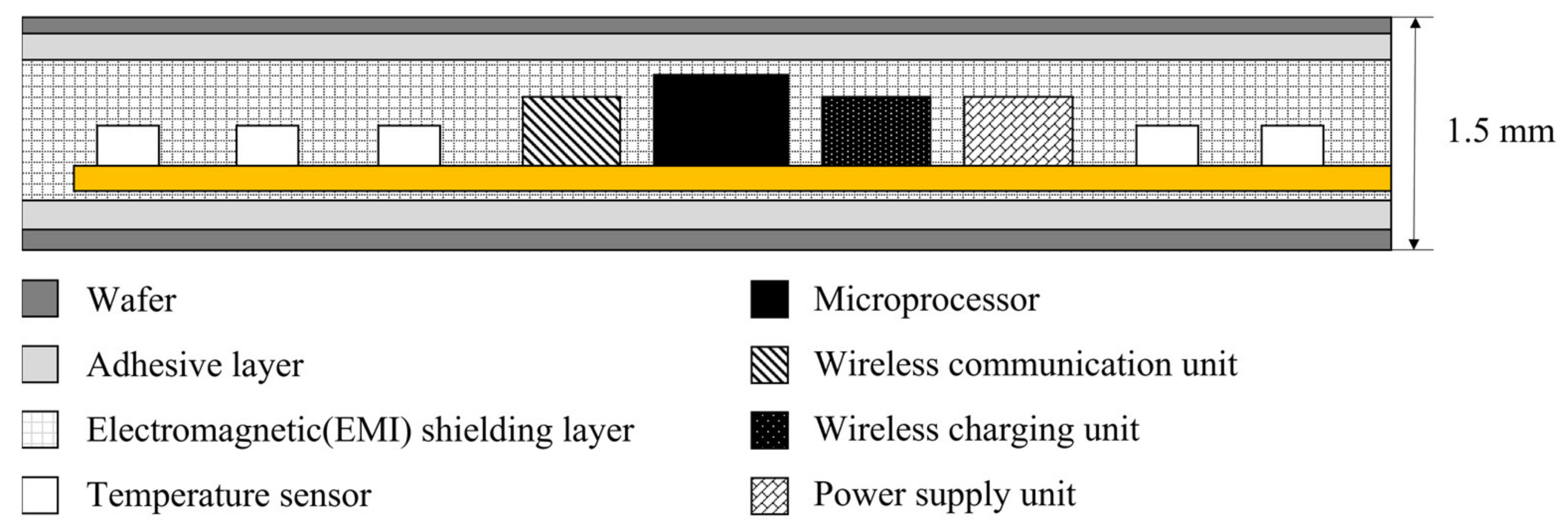
OTMS operates inside the vacuum chamber to acquire temperature data for the ESC functional test, and data acquisition, temporal storage, and wireless communication outside the chamber are required. Infrared communication standards are considered to implement a two–way wireless communication. A pair of photodiodes and infrared (IR) LEDs with wavelength is longer than 1.2 μm for IR communication with a data reader through a silicon wafer. A lithium battery was used as an electrical power source to operate the electronics of OTMS. Besides the electronics, we considered the thickness of the OTMS to be thin enough (<1.5 mm) to be safely carried by the wafer handler robot for the system automation. Note that the overloaded wafer handler turns on an interlock alarm in current 300 mm production tools to prevent any potential wafer breakage at the slit door from the drooping of the handler arm.
The ESC operational mechanism is an electrostatic force formed between wafer and chuck as the name stands for, and the electrostatic force can be formed by monopolar or bipolar type electrodes. To prevent the electric field effect on the temperature measuring electronic circuits on the ESC, electromagnetic interference shielding must protect electronic circuits. Electromagnetic waves from the plasma with an RF power source should also be considered when it is exposed to plasma. Film-type Cu and Ni alloy metal mesh were used to block electromagnetic waves.
As shown in Figure 2, wafer-type sensor assembly was based on the silicon wafer cavity in its structure where the TMUs and controller circuits are located. The round edge area remained while most of the area was partially removed to ensure the mechanical strength of 300 mm wafers. Space between two wafers was filled with fillers and bonding materials (thermosetting resin, and silicone-based materials were used). The structure of the sensor was designed to be free from particle contamination when it is inserted into the test or process chamber.

3. System Design

3.1. Sensing Unit

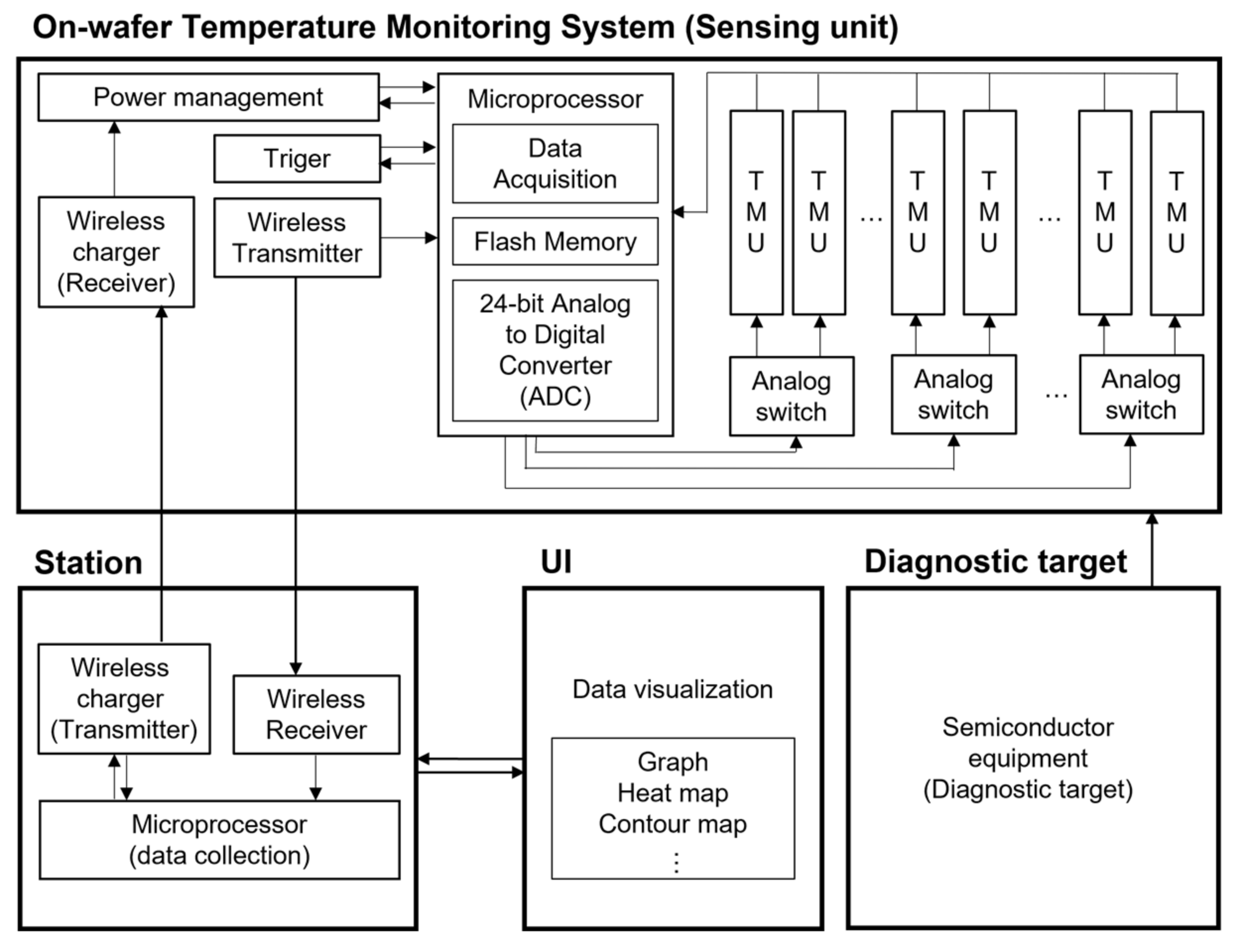
The proposed sensor system consists of three parts, namely a sensing unit, station, and user interface. The sensing unit consists of 65 TMUs and a microprocessor unit (MPU, Analog Devices ADUCM363, Norwood, MA, USA), managing the data acquisition, local memory storage, and data transmission. The station has another MPU circuit for both data receiving and battery charging functions. The user interface (UI) provides data visualization applications, such as temperature graphs of the sensor, wafer heat map, contour map, and summary reports. The system block diagram of the proposed on-wafer type temperature monitoring sensor system is shown in Figure 3. Current signals from the 64 TMUs are fed into the multiplexer via operational amplifiers and an analog to digital converter (Analog Devices ADG1606), and MCU controls all the operations and records the measured temperature data in flash memory. Once the data recording is carried out, the OTMS is transferred to the station, and the MCU in the station performs IR data communication. Under the bias condition for chucking and processing, the electronic circuits of the sensor can be vulnerable to signal noise and delay induced by other process chamber parts. A high-performance ICs capable of preventing static electricity was used to protect the circuit from static power. The sensing unit often operate in a high temperature environment, so thermal shut down must be considered. Therefore, we adopted a regulator (Texas Instruments TPS62088, Dallas, TX, USA) with a thermal shut down circuit for safety.

3.2. Film Battery and Charging Circuit

While the data transfer proceeds, wireless battery charging is simultaneously made for the next use. Typical electronic products use lithium polymer batteries. The structure of a lithium polymer battery consists of a liquid-type electrolyte between the anode and the cathode, which is packed under a vacuum with an aluminum film to prevent the electrolyte from escaping. Under vacuum conditions during the ESC wafer chucking step, air bubbles in the electrolyte of the lithium polymer battery expand, causing the pouch to swell and break the two bonded wafers (Figure 4a). Instead, since the electrolyte is composed of solid powder, a solid type battery has the advantage of no visible expansion of the battery pouch (Figure 4b). However, the charging rate of the all-solid battery was noticeably slow, making it difficult to use in the proposed system. Therefore, we used a semi-solid battery to prevent the battery pouch from expanding in a vacuum. Considering the aforementioned OTMS’s hardware consideration, the developed prototype of the sensor circuit diagram is shown in Figure 5a,b.

3.3. Station and User Interface Software

Besides the OTMS, we used a 300-mm front opening universal pod (FOUP) for the station applicable to an automatic wafer handling robot. The transmitter LED is used to set the recipe for the data acquisition in the station, and the station also has a receiver LED, which is controlled by UI software. When the OTMS is transferred to the station, the 300 mm FOUP in this experiment and the battery for OTMS are automatically charged inside the station. A schematic for the station and PC-controlled UI is shown in Figure 6. The UI is designed using C++ in Visual Studio. The main function of the UI is to visualize the temperature data of the OTMS as a graph and temperature map. Contour maps are also included for a more convenient viewing of the temperature distribution.

4. System Verification

The temperature sensor we used is an analog RTD-type sensor, and temperature calibration is required. In this study, measurements were made only at specific temperature points, so two-point calibrations were performed at 60 °C and 80 °C since the operational temperature prevails between 40 °C and 80 °C. We calibrated in a proven oven calibrated at the highest possible temperature. The formula used for calibration is as follows.
y 60   C = a x 1 + b
y 80   C = a x 2 + b
By using the actual 60 °C and 80 °C measurement data x1 and x2, we added a slope and constant to the UI so that we can fit it to 60 °C and 80 °C, respectively. The ESC temperature measurement data before and after calibration can be checked in Figure 7.
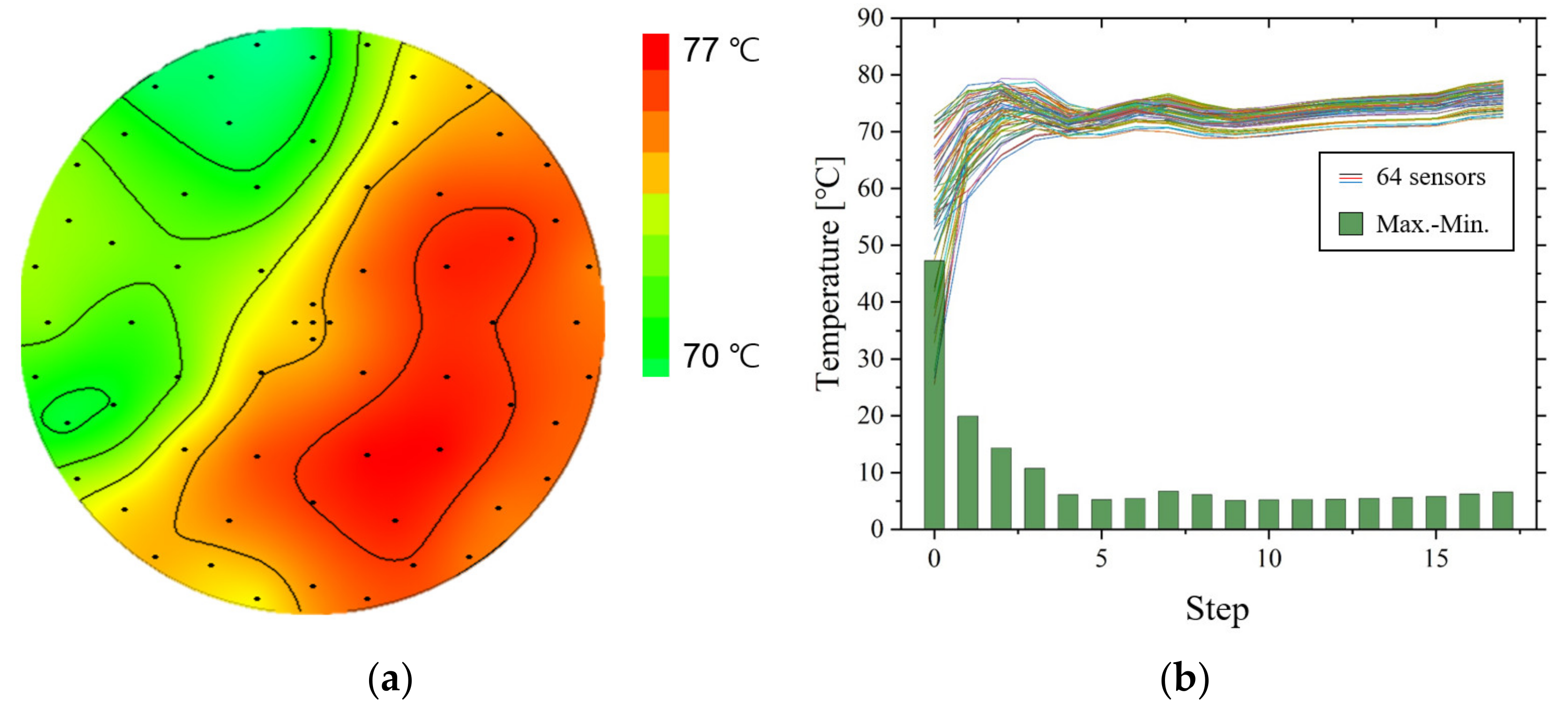
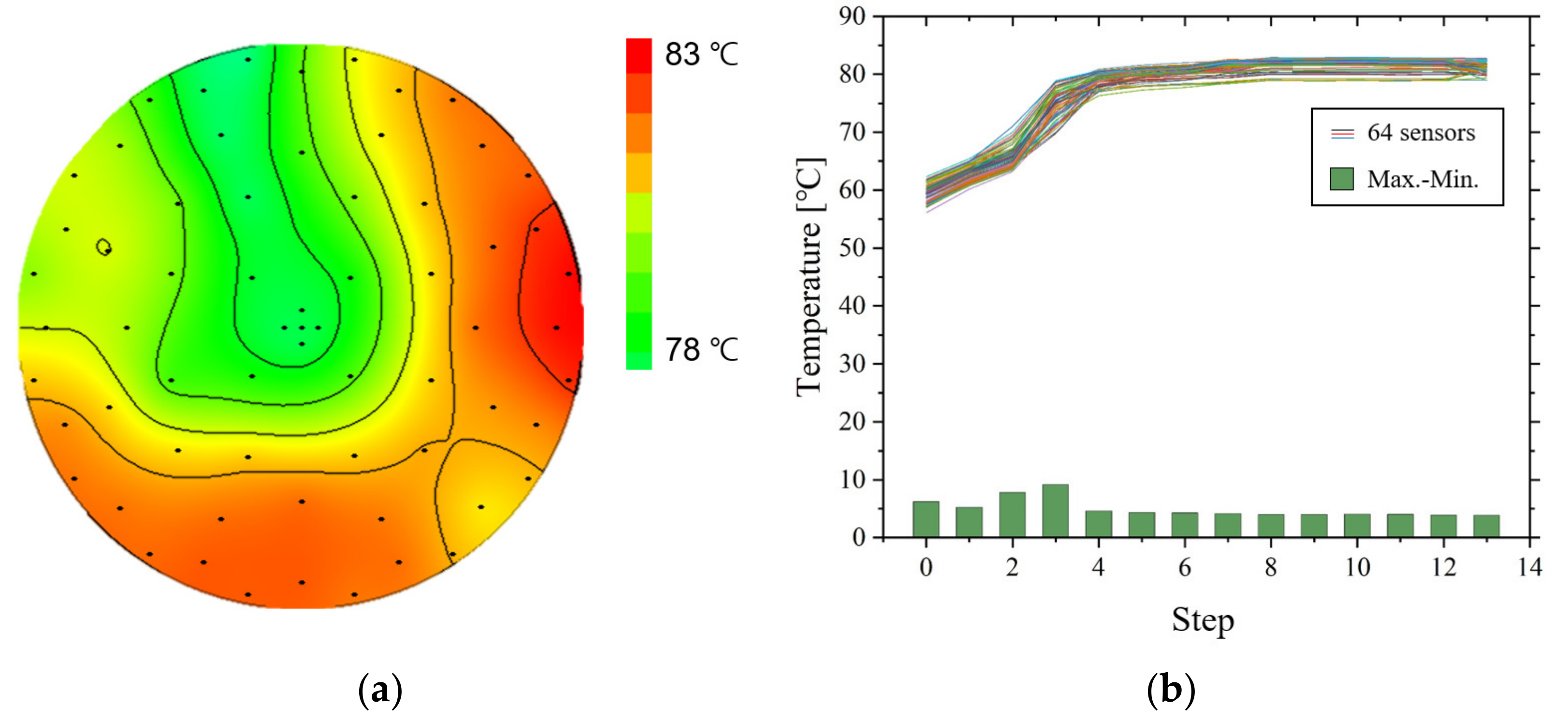
We tested the OTMS in an ESC test chamber. The equipment configuration is shown in Figure 8. The ESC test chamber is configured to check the operational status of the ESC. The main functions of ESC, such as temperature control, electrostatic power applications, and helium gas supply, are implemented in vacuum conditions. The test recipe applied 80 °C ESC temperature, 20 °C cooling path temperature, 2000 V chucking force, and 10 sccm He flows. The experiment measured the temperature distribution of failure for the ESC in an ESC test chamber. Then, the temperature distribution of the repaired ESC was measured in the same recipe and environment. The shape of the temperature data of the failure ESC measured by the OTMS is shown in Figure 9. The temperature deviation of bad ESC under the same temperature is expressed as ±5.61 °C. When it is repaired, the temperature distribution is the same as in Figure 10. The temperature deviation is shown to decrease by ±3.83 °C. Therefore, changes in the temperature distribution before and after repair of the ESC can be observed and the abnormal state of the ESC can be determined.

5. Conclusions

The temperature variation of the ESC has a direct impact on the characteristics of the etching process. First, the etch rate of the center and edge may differ, depending on the characteristics of the thin film. Second, there is a correlation between the ESC temperature distribution and the CD map. Generally, the lower the ESC temperature, the lower the CD line value [39]. Therefore, temperature control of the ESC is critical, and a diagnostic device that can accurately measure the temperature distribution of the ESC is required.
A wireless temperature distribution measurement system was developed to precisely monitor the abnormal state of the ESC. The proposed system is manufactured with a thickness of 1.5 mm, which is the thickness of two wafers to meet the wafer handling automation requirements of semiconductor chip manufacturers. The OTMS has 65 TMUs and a driving circuit that includes the MCU, battery, wireless battery charging, and wireless communication function, indicating that the temperature distribution can be measured under real-world process conditions without opening the chamber. The OTMS can be used for approximately 20 min on a single charge. In this experiment, we checked the data before and after ESC repair, and it was confirmed that the abnormal state of the ESC can be diagnosed using the temperature distribution diagram. OTMS could be manufactured with a simple manufacturing process compared to commercially sensors developed in the past. Commercial sensors should be manufactured using semiconductor processes (etching, sputtering, deposition, etc.). However, OTMS is manufactured based on a PCB board, so fabrication is simple.
However, the proposed OTMS still has limitations in measuring the temperature distribution in the plasma-on state in actual equipment sine no IC has an electromagnetic shielding function. Electromagnetic shielding requires electromagnetic shielding of the entire IC, leads, and transmission line. When an insulating coating is applied and a shielding film is formed to prevent a short circuit, the electromagnetic wave shielding metal penetrates the insulating film due to the interfacial properties. Additional research on electromagnetic wave shielding, such as electromagnetic wave shielded sputtering or metal strips, can solve this problem [40,41]. Furthermore, OTMS uses optical communication-based communication standards and wireless coil charging methods. It requires alignment in pairs, so the alignment point is actually two points. Therefore, alignment is difficult when wafers are unloaded from the ESC or chamber and then placed into a station. The position of the charging coil system and the position of the communication element are aligned with the origin of the sensor system to solve the problem of having two alignment points. A wafer-type temperature measurement system that can measure in a plasma state can be realized if the insulating coating is made consistently relating to the electromagnetic wave shielding problem.

Author Contributions

Conceptualization, principal investigation, supervision, funding acquisition, writing review and editing, S.J.H.; methodology, electronics and hardware design, data acquisition, writing original draft preparation, J.-H.K. Firmware programming and UI design and data acquisition, Y.K. and W.S. All authors have read and agreed to the published version of the manuscript.

Funding

This work was supported by Advanced Institute of Convergence Technology (GID: AICT 006-T1) and Korea Institute of Advancement for Technology (KIAT) grant funded by Korean Government (MOTIE). (P0008458, The Competency Development Program for Specialist).

Institutional Review Board Statement

Not applicable.

Informed Consent Statement

Not applicable.

Data Availability Statement

Experimental data are available upon request.

Acknowledgments

Authors are grateful to staff of Semiconductor Process Diagnosis and Research Center (SPDRC) at Myongji University for their professional management of 300 mm wafer fabrication equipment.

Conflicts of Interest

The authors declare no conflict of interest.

References

  1. Yugma, C.; Blue, J.; Dauzère-Pérès, S.; Obeid, A. Integration of Scheduling and Advanced Process Control in Semiconductor Manufacturing: Review and Outlook. J. Sched. 2015, 18, 195–205. [Google Scholar] [CrossRef]
  2. Abe, H.; Yoneda, M.; Fujiwara, N. Developments of Plasma Etching Technology for Fabricating Semiconductor Devices. Jpn. J. Appl. Phys. 2008, 47, 1435–1455. [Google Scholar] [CrossRef]
  3. Baek, K.H.; Coonan, B.; Carbery, M.; Joo, J.; Woo, H.; Lee, T.S.; An, H.S.; Koo, Y.; Han, C.; Han, S.; et al. Process and Chamber Health Monitoring of Plasma Enhanced Ti Deposition Process through High Performance VI-probe. In Proceedings of the 2007 International Symposium on Semiconductor Manufacturing, Santa Clara, CA, USA, 15–17 October 2007; pp. 1–4. [Google Scholar]
  4. Kang, G.; An, S.; Kim, K.; Hong, S. An In Situ Monitoring Method for PECVD Process Equipment Condition. Plasma Sci. Technol. 2019, 21, 064003. [Google Scholar] [CrossRef]
  5. Lee, Y.; Kim, C.; Hong, S.J. Industrial Internet of Things for Condition Monitoring and Diagnosis of Dry Vacuum Pumps in Atomic Layer Deposition Equipment. Electronics 2022, 11, 375. [Google Scholar] [CrossRef]
  6. Hong, S.J.; Lim, W.Y.; Cheong, T.; May, G.S. Fault Detection and Classification in Plasma Etch Equipment for Semiconductor Manufacturing e-Diagnostics. IEEE Trans. Semi. Manufac. 2011, 25, 83–93. [Google Scholar] [CrossRef]
  7. Yang, R.; Chen, R. Real-Time Plasma Process Condition Sensing and Abnormal Process Detection. Sensors 2010, 10, 5703–5723. [Google Scholar] [CrossRef] [Green Version]
  8. Sana, M.; Saleem, U.; Farooq, M.; Qamar, A.; Bhutta, M.M.A.; Zafar, S. Identification of Failure Modes on Electrostatic Chuck through Reliability Centered Maintenance: A Case Study: Identification of Failure Modes on ESC through RCM. Proc. Pak. Acad. Sci. A 2018, 55, 21–32. [Google Scholar]
  9. Lee, H.J.; Lee, S.H. Numerical Evaluation on Surface Temperature Uniformity of Multi-zone and Single-zone Ceramic Heaters with the Electrostatic Chuck. J. Mech. Sci. Technol. 2021, 35, 3763–3770. [Google Scholar] [CrossRef]
  10. Lewin, L.; Plummer, J.; Ward, R. Electrostatic Chuck. U.S. Patent 4,502,094, 26 February 1985. [Google Scholar]
  11. Hartsough, L. Electrostatic Wafer Holding. Solid State Technol. 1993, 36, 87–90. [Google Scholar]
  12. Wright, D.; Chen, L.; Federlim, P.; Forbes, K. Manufacturing Issues of Electrostatic Chucks. J. Vac. Sci. Technol. B 1995, 13, 1910–1916. [Google Scholar] [CrossRef]
  13. Asano, K.; Hatakeyama, F.; Yatsuzuka, K. Fundamental Study of an Electrostatic Chuck for Silicon Wafer Handling. IEEE Trans. Ind. Appl. 2002, 38, 840–845. [Google Scholar] [CrossRef]
  14. Yuchun, S.; Jia, C.; Yijia, L.; Yuemin, H.; Limhong, J. Design Space of Electrostatic Chuck in Etching Chamber. J. Semiconduct. 2015, 36, 084004. [Google Scholar]
  15. Brcka, J.; Jones, B.; Leusink, G.; Long, J.; Oliver, B.; Tweed, C. Method for Characterizing the Performance of an Electrostatic Chuck. U.S. Patent 6,853,953 B2, 8 February 2005. [Google Scholar]
  16. Yoshioka, K.; Takahashi, S.; Sasaki, Y. Method and Apparatus for Repairing an Electrostatic Chuck Device, and the Electrostatic Chuck Device. U.S. Patent 8,252,132 B2, 28 August 2012. [Google Scholar]
  17. Raj, C.; Hirahara, R. Methods and Apparatus for Electrostatic Chuck Repair and Refurbishment. U.S. Patent 9,349,630 B2, 24 May 2016. [Google Scholar]
  18. Raj, C.; Hirahara, R. Methods and Apparatus for Electrostatic Chuck Repair and Refurbishment. U.S. Patent 10,049,908 B2, 14 August 2018. [Google Scholar]
  19. Boyd, W. New Repair Method for Electrostatic Chuck. U.S. Patent 0166311 A1, 14 June 2018. [Google Scholar]
  20. Parkhe, V.; Narendrnath, K. Electrostatic Chuck Optimized for Refurbishment. U.S. Patent 10,056,284 B2, 21 August 2018. [Google Scholar]
  21. Kim, O.; Kim, O. Electrostatic Chuck and Method for Manufacturing Electrostatic Chuck. U.S. Patent 10,347,520 B2, 9 July 2019. [Google Scholar]
  22. Parkhe, V. Sensor System for Multi-Zone Electrostatic Chuck. U.S. Patent 10,582,570 B2, 3 March 2020. [Google Scholar]
  23. Hart, A.; Boyd, J.; Palma, L.; Dent, A. Electrostatic chucks and methods for refurbishing same. U.S. Patent 8,597,448, 3 December 2013. [Google Scholar]
  24. Shih, H. Method of refurbishing bipolar electrostatic chuck. U.S. Patent 8,291,565, 23 October 2012. [Google Scholar]
  25. Huslla, I.; Enke, K.; Grunwald, H.; Lorenz, G.; Stoll, H. In Situ Silicon-Wafer Temperature Measurements during RF Argon-Ion Plasma Etching via Fluoroptic Thermometry. J. Phys. D Appl. Phys. 1987, 20, 889–896. [Google Scholar] [CrossRef]
  26. Cardoso, A.; Srivastava, A. Improvements in Wafer Temperature Measurements. J. Vac. Sci. Technol. B 2001, 19, 397–402. [Google Scholar] [CrossRef]
  27. Adams, B.; Schietinger, C. In-Situ Optical Wafer Temperature Measurement. AIP Conf. Proc. 2003, 684, 1081–1086. [Google Scholar]
  28. Tan, W.; Tang, J.; Loh, A.; Tay, A. In Situ Measurement of Wafer Temperature Using Two Sensors with Different Dynamical Properties. Meas. Sci. Technol. 2006, 17, 2957–2963. [Google Scholar] [CrossRef]
  29. Kumar, V.; Verma, J.; Maan, A.S.; Akhtar, J. Epitaxial 4H–SiC based Schottky diode temperature sensors in ultra-low current range. Vacuum 2020, 182, 109590. [Google Scholar] [CrossRef]
  30. Kumar, V.; Maan, A.; Akhtar, J. Barrier Height Inhomogeneities Induced Anomaly in Thermal Sensitivity of Ni/4H-SiC Schottky Diode Temperature Sensor. J. Vac. Sci. Technol. B 2014, 32, 041203. [Google Scholar] [CrossRef]
  31. Pan, S.; Gürleyük, Ç.; Pimenta, M.; Makinwa, K. 10.3 A 0.12 mm 2 Wien-Bridge Temperature Sensor with 0.1 °C (3σ) Inaccuracy from −40 °C to 180 °C. In Proceedings of the 2019 IEEE ISSCC, San Francisco, CA, USA, 17–21 February 2019. [Google Scholar]
  32. Tseng, S.; Chen, M. Yield Enhancement in Stripper Process and Related Process using SensArray HighTemp Wafer. In Proceedings of the SEMI Advanced Semiconductor Manufacturing Conference, New York, NY, USA, 16–19 May 2016. [Google Scholar]
  33. Kim, D.; Kim, J.; Chu, D.; Hong, D. Measuring the Wafer Temperature in HVM Process Tools Using a New Approach with Automated Wireless HighTemp-400 and EtchTemp-SE Wafer Systems. In Proceedings of the 29th SEMI Advanced Semiconductor Manufacturing Conference, New York, NY, USA, 30 April–3 May 2018. [Google Scholar]
  34. Fang, F.; Vaid, A.; Vinslava, A.; Casselberry, R.; Mishra, S.; Dixit, D.; Timoney, P.; Chu, D.; Porter, C.; Song, D.; et al. Correlation Study of Actual Temperature Profile and In-line Metrology Measurements for Within-Wafer Uniformity Improvement and Wafer Edge Yield Enhancement. In Proceedings of the Metrology, Inspection, and Process Control for Microlithography XXXII, Los Angeles, CA, USA, 21 March 2018. [Google Scholar]
  35. Lee, J.; Siegal, D.; Lapira, E. Development of a Predictive and Preventive Maintenance Demonstration System for a Semiconductor Etching Tool. ESC Trans. 2013, 52, 913–927. [Google Scholar] [CrossRef]
  36. Im, D.; Min, W.; Hong, S. Planar Heating Chuck to Improve Temperature Uniformity of Plasma Processing Equipment. Jpn. J. Appl. Phys. 2020, 59, SJJD01. [Google Scholar] [CrossRef]
  37. Park, Y.; Du, H.; Im, D.; Hong, S. Hardware Design for Cryogenic Etching Equipment. Heat Transf. Res. 2021, 52, 8. [Google Scholar] [CrossRef]
  38. Matula, R. Electrical Resistivity of Copper, Gold, Palladium, and Silver. J. Phys. Chem. Ref. Data 1979, 8, 1147–1298. [Google Scholar] [CrossRef] [Green Version]
  39. Newby, J.; Bieli, G.; Wollenweber, M.; Melzer, R.; Nogatz, T.; Sobe, J. Correlation Study of Spatial ESC Temperature Profile and Optical CD/CD SEM Measurements to Investigate Silicon Recess and Gate CD after Etch. In Proceedings of the 25th Annual SEMI ASMC2014, New York, NY, USA, 19–21 May 2014. [Google Scholar]
  40. Park, J.; Lee, J.; Choi, H.; Jang, W.; Kim, T.S.; Suh, D.; Suh, S. Electromagnetic Interference Shielding Effectiveness of Sputtered NiFe/Cu Multi-layer Thin Film at High Frequencies. Thin Solid Films 2019, 677, 130–136. [Google Scholar] [CrossRef]
  41. Aiello, O.; Fiori, F. On the Susceptibility of Embedded Thermal Shutdown Circuit to Radio Frequency Interference. IEEE Trans. Electromag. Compat. 2011, 54, 405–412. [Google Scholar] [CrossRef]
Figure 1. TMU locations and overall structure of OTMS.
Electronics 11 00880 g001
Figure 2. Structure of OTMS.
Electronics 11 00880 g002
Figure 3. Block diagram of OTMS.
Electronics 11 00880 g003
Figure 4. Results of operation test in a vacuum. (a) OTMS damaged due to the expansion of lithium polymer type battery, (b) semi-solid type battery vacuum test.
Electronics 11 00880 g004
Figure 5. Prototype of OTMS. (a) Hardware design of OTMS, (b) circuit schematic of OTMS.
Electronics 11 00880 g005
Figure 6. OTMS and UI image during data transmission/reception at the station.
Electronics 11 00880 g006
Figure 7. Graphs of before and after temperature calibration that ESC temperature distribution: (a) Sensor location of 2nd TMU, 3rd TMU, and 14th TMU and (b) graph of before and after temperature.
Electronics 11 00880 g007
Figure 8. Schematic of ESC temperature distribution measurement test.
Electronics 11 00880 g008
Figure 9. Abnormal ESC temperature distribution measurement distribution diagram: (a) heat map and contour map and (b) temperature measurement graph.
Electronics 11 00880 g009
Figure 10. After repair ESC temperature distribution measurement distribution diagram: (a) heat map and contour map and (b) temperature measurement graph.
Electronics 11 00880 g010
Publisher’s Note: MDPI stays neutral with regard to jurisdictional claims in published maps and institutional affiliations.