Article

A 130-to-220-GHz Frequency Quadrupler with 80 dB Dynamic Range for 6G Communication in 0.13-μm SiGe Process

1
School of Microelectronics, and Engineering Research Center of Integrated Circuits for Next-Generation Communications, Ministry of Education, Southern University of Science and Technology, Shenzhen 518055, China
2
State-Key Laboratory of ASIC and System, Fudan University, Shanghai 201203, China
3
School of Physics and Technology, Wuhan University, Wuhan 430072, China
*
Authors to whom correspondence should be addressed.
Electronics 2022, 11(5), 825; https://doi.org/10.3390/electronics11050825
Submission received: 29 January 2022 / Revised: 28 February 2022 / Accepted: 2 March 2022 / Published: 7 March 2022
(This article belongs to the Special Issue Feature Papers in "Networks" Section)

Abstract

:
This paper presents a broadband frequency quadrupler (FQ) implemented with a standard 130-nm SiGe BiCMOS process. Two broadband push-push frequency doublers (×2) operate at an input frequency of 32.5–55 GHz and 65–110 GHz, respectively. To properly drive the two doublers with enough input power and bandwidth, two transformer coupled power amplifiers (PAs) have been adopted. The former power amplifier is based on a neutralized capacitor structure and the latter is based on a transformer topology. A nonlinear device model and a systematic methodology to generate maximum power at second harmonic are proposed. By manipulating the device nonlinearity and optimizing the magnetically and capacitively coupled resonator (MCCR) matching networks, optimum conditions for harmonic power generation are provided. The measurement results show that the proposed quadrupler provides a 90-GHz bandwidth with an 80-dB dynamic range and a high energy efficiency η of 3.7% at 210 GHz.

1. Introduction

Due to the progress of SiGe BiCMOS technologies, the working frequency of semiconductor devices is increasing, 6G sub-THz circuits can be implemented based on these devices. Compared to GaAs and GaN processes, the SiGe BiCMOS technologies are capable for higher integration and lower power consumption, which is crucial for portable devices with compact size. Various solid-state circuits have been implemented in SiGe technologies [1,2,3,4], such as the CML divider (Current Mode Logic divider) [5], transimpedance amplifier [6], voltage-controlled oscillators (VCOs) [7], bandpass filter [8], and switch [9]. Including the above various blocks based on the SiGe BiCMOS process, they have been widely used in various sub-THz systems, including radar receivers [10], 5G transceiver [11], and high-resolution imaging device [12].
A wideband signal source with high dynamic range and stability is essential for these systems. Due to high frequency effects, including substrate loss and serious parasitic effects, and the decrease of transistor’s ft/fmax, it is difficult to realize a broadband high frequency signal source with a low phase noise and high dynamic range. To overcome the above disadvantages, accurately modeling for transistors and passive devices is important. In this paper, the device modeling and circuit analysis are analyzed to realize optimum matching networks and to optimize the second harmonic output power.
There are three methods to generate a wideband sub-THz signal. One method involves a sub-THz wideband VCO. However, the phase noise of the sub-THz VCO is seriously degraded due to the above high frequency effects and the frequency is modulated with temperature. To maintain the frequency, the phase-locked loop (PLL) is necessary, and the power consumption is large. The second method involves a narrowband VCO with relatively good phase noise. However, several PLLs must be utilized to realize a large frequency range. Thus, the power consumption is large. Instead of utilizing several PLLs to generate an ultra-wideband frequency, a frequency multiplier generating Nth harmonic by only low frequency PLL is a good solution [13,14,15,16,17,18]. Traditionally, a power amplifier can generate the desired Nth harmonic multiplied signal with undesired harmonics removed via a filter. Another technique is the linear superposition (LS) technique, which adds up the multiple-phase waves to construct the harmonic output. However, the efficiency (η) of these methods is low and the bandwidth is limited.
In this paper, two PAs with different bandwidths have been used to drive the frequency doublers, which enable the broadband response up to 220 GHz. The broadband signal generator in 0.13-μm silicon-germanium (SiGe) technology has used magnetically and capacitively coupled resonator (MCCR) matching networks. Thus, the second harmonic matching power is enlarged. We report the design and measurement results of the wideband FQ circuits with a bandwidth of 90 GHz and a peak output power of 2.5 dBm in a commercial 130-nm SiGe BiCMOS technology. The measurement results show that the proposed quadrupler provides a 90-GHz bandwidth with an 80-dB dynamic range and η of 3.7% at 210 GHz. In Section 2, the adopted 130-nm SiGe BiCMOS technology and device model are briefly discussed. Section 3 presents a working principle of the doubler, matching network and design of the FQ at 130–220 GHz, including the PAs and two wideband doublers. The measurement results of the FQ are presented in Section 4 and are also compared with prior state-of-the-art works. Finally, the conclusion is given in Section 5.

2. The Process of the 130-nm SiGe BiCMOS Technology and Device Modeling

It can be seen from the back-end-of-the-line (BEOL) cross section in Figure 1 that the thickness of the top two-layer metals is the thickest among all available metal layers. The process is highly suitable for various mm-wave and THz circuits. The EM (Electromagnetic) simulation environment in HFSS (High Frequency Structure Simulator) software is further supported by the process. The main material of the top two layers is copper which has low resistivity and can be utilized for a passive-device design. The metal layers enable the customized realization of a high-quality inductor, transformer, and transmission line, such as a microstrip and coplanar line.
To reduce the losses of metal interconnections of the double balanced mixer and improve the current carrying capacity of the connecting line at Sub-THz range, the top two metals, which have higher current densities and lower sheet resistance, are adopted. The connecting metals and vias should reduce the parasitic effects between multi-layer metals. Therefore, the connection between the active devices and passive devices are shown in Figure 2. The proposed connection can significantly improve the RF (Radio Frequency) performance. In addition, compared to a standard CMOS process, a SiGe process provides high-performance hetero-junction bipolar transistors (HBTs) that exhibit ft/fmax of 300/500 GHz and breakdown voltages of BVCEO = 1.5 V and BVCBO = 5 V, respectively.
The device model of the HBTs is shown in Figure 3. g m is the transconduance of the devices, and C b c is the capacitance between the collector and the base. Due to C b e , there is a crossover between the input and output of the transistor, which shows the miller effect and reduces the stability of the transistor. Then, we can formulate the equations from the small signal model diagram:
The model includes the intrinsic parameters of HBT devices without the parasitic parameters of interconnections. The intrinsic parameters of a small signal equivalent circuit model can be directly extracted by de-embedding and using the Y-parameter. The Y-parameter matrix of the intrinsic model can be calculated as follows [19,20,21]:
Y 11 = g b e + j ω C b e + j ω C b c 1 + r b b g b e + j ω C b e + j ω C b c  
Y 12 = j ω C b c 1 + r b b g b e + j ω C b e + j ω C b c
Y 21 = g m j ω C b c 1 + r b b g b e + j ω C b e + j ω C b c
Y 22 = g c e + j ω C b c + j ω C c s + g m j ω C b c j ω C b c r b b   1 + r b b g b e + j ω C b e + j ω C b c .
The proposed FQ utilizes two cascaded doublers to obtain conversion power gain, however it will be limited by the cut-off frequency ft, which is described by current amplification factor β decreasing to 1 for the common emitter configuration. In order to improve the gain, the active devices and passive devices are both optimized. Passive device modeling is an important part for FQ design because these devices are utilized for the input/output and inter-stage matching. Generally, the manufactory provides some standard models of the capacitors, inductors, and transmission lines. However, the required accurate frequency of these models is up to 20 GHz and these models cannot meet the requirements of the proposed Sub-THz circuit design. The connecting lines between the HBTs contribute inductance and capacitance whose patterns are determined by the layout of the chip. Thus, it is essential to customize design and model passive devices and connecting lines based on the microwave circuit for optimum matching among the HBT.

3. The Proposed FQ Circuits

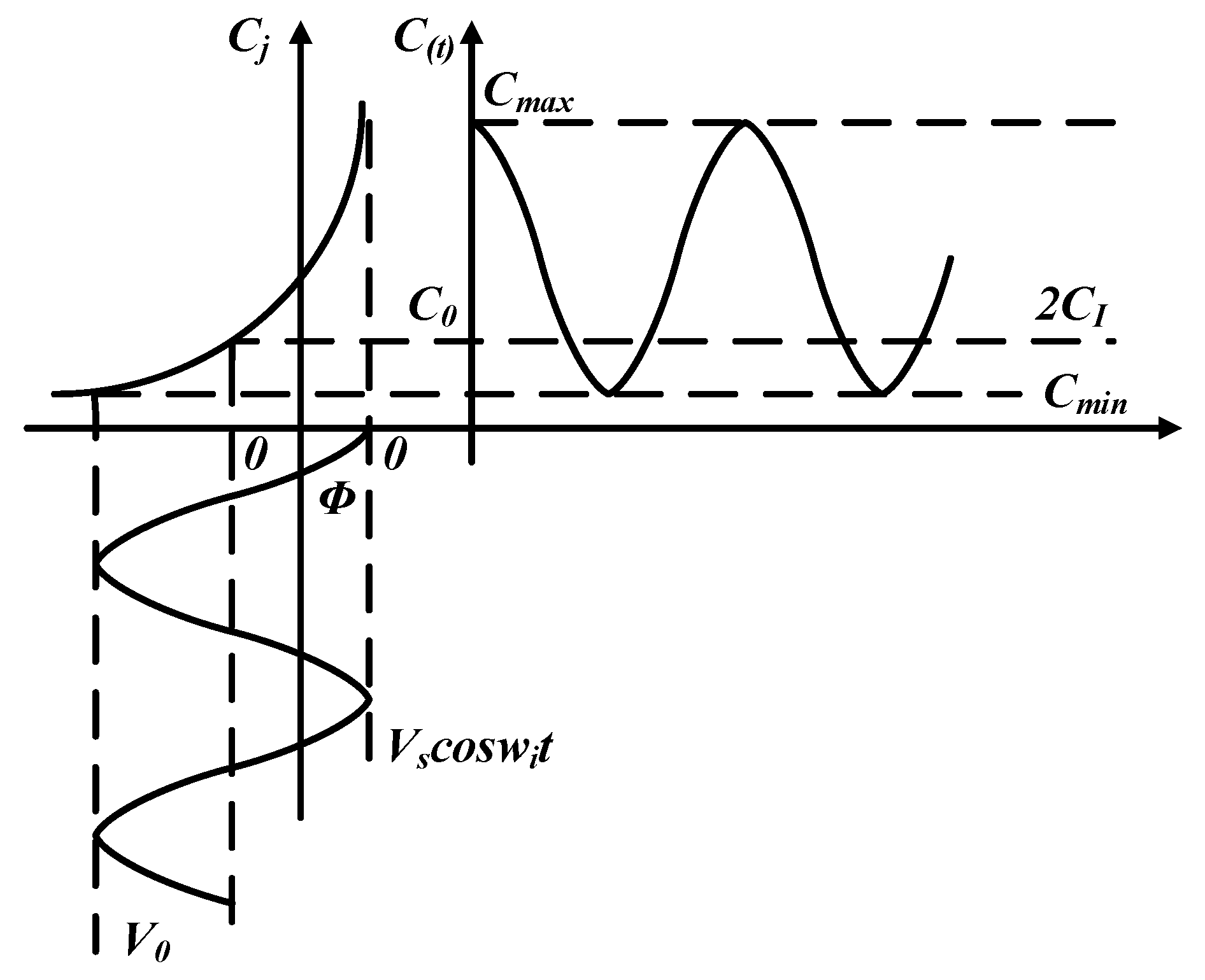
3.1. The Working Principle of the Frequency Doubler

The working principle of the doubler is using a nonlinear device. Making the input sine wave pass through the nonlinear device, and the output waveform will be distorted to produce various harmonics. Then, the filter circuit is used to extract the required harmonic to obtain the required terahertz signal. A simple nonlinear network is formed by a two terminal nonlinear capacitor, which is formed by the collectors of the SiGe devices. Taking the varactor as an example, the nonlinear characteristics of diode junction capacitance is briefly described. If the epitaxial layer of the diode is uniformly doped, then the junction charge function is where C j 0 is the zero-bias junction capacitance, V is the junction voltage, and the diffusion potential is the difference of the work function between the anode metal and the semiconductor of the diode, then the small signal junction capacitance is:
C V   = 2 C j 0 1 V   .
Among them, if C j 0 is the zero bias junction capacitance, V is the junction voltage, and the diffusion potential is the difference of the work function between the diode metal and the semiconductor, then the small signal junction capacitance is:
C V   = d Q V d V = C j 0 1 V 1 2 .
If the epitaxial layer of HBTs’ collector is non-uniformly doped and has certain regularity, the expression of junction capacitance can be obtained by changing the index of the denominator of Formula (5). γ is strongly related to the doping concentration distribution of the epitaxial layer, which is not suitable for a large reverse voltage range when the doping is very uneven and can be expressed by different parameters:
C V   = d Q V d V = C j 0 1 V γ   .
Suppose that the varactor diode external excitation is V = V O + V s c o s ω t . By substituting it into the general expression of varactor junction capacitance, we can get Formula (8):
C t = C j 0 1 V O + V s c o s ω t γ   .
The corresponding junction capacitance curve with nonlinearity is shown in Figure 4. As shown as in Figure 5, the nonlinear capacitors can be formed by connecting the col-lectors of the two HBTs with the differential voltage source [19]. If the frequency doubling is required, the HBTs’ collector generally needs to be applied with a bias voltage to make the HBTs work in the nonlinear state, and the output current will generate high-order harmonics. The excitation signal is provided by the front-end stage with differential signals V i + , V i . The charge of the two terminal nonlinear capacitors can be expanded in power series:
Q = a 0 + a 1 V i + a 2 V i 2 + a 3 V i 3 +   .
Assuming V i + = V + c o s ω t , V i = V c o s ω t , then:
Q A = a 0 + 1 2 a 2 V + 2 +   a 1 V + + 3 4 a 3 V + 3 c o s ω t + 1 2 a 2 V + 2 c o s 2 ω t +
Q B = a 0 + 1 2 a 2 V 2 +   a 1 V + 3 4 a 3 V 3 c o s ω t + 1 2 a 2 V 2 c o s 2 ω t + .
When the excitation of the nonlinear network is a single tone cosine signal, Formula (11) shows that the circuit response contains the dependent nonlinearity. By using the filter circuit and impedance matching circuit, the specific harmonic components can be extracted from each harmonic. Q = Q B + Q A is in some symmetrical circuit topologies and only contains even terms, then the circuit response will only produce second harmonics.
The passive devices realized filter utilizes the transformer. The magnetic field of the transformer is mainly limited in the primary coil and secondary coil, so the surrounding ground has little influence on the electromagnetic field. At the same time, only a small part of the magnetic field passes through the silicon substrate, so most of the energy of the transformer is transferred from the primary coil to the secondary coil through coupling. The differential structure of the transformer ensures there is a better common mode signal suppression and reduces the impact on the power supply and ground. The bias voltages of doublers are fully designed to generate the highest power of second harmonic by maximizing the second harmonic current and impedance at this frequency.

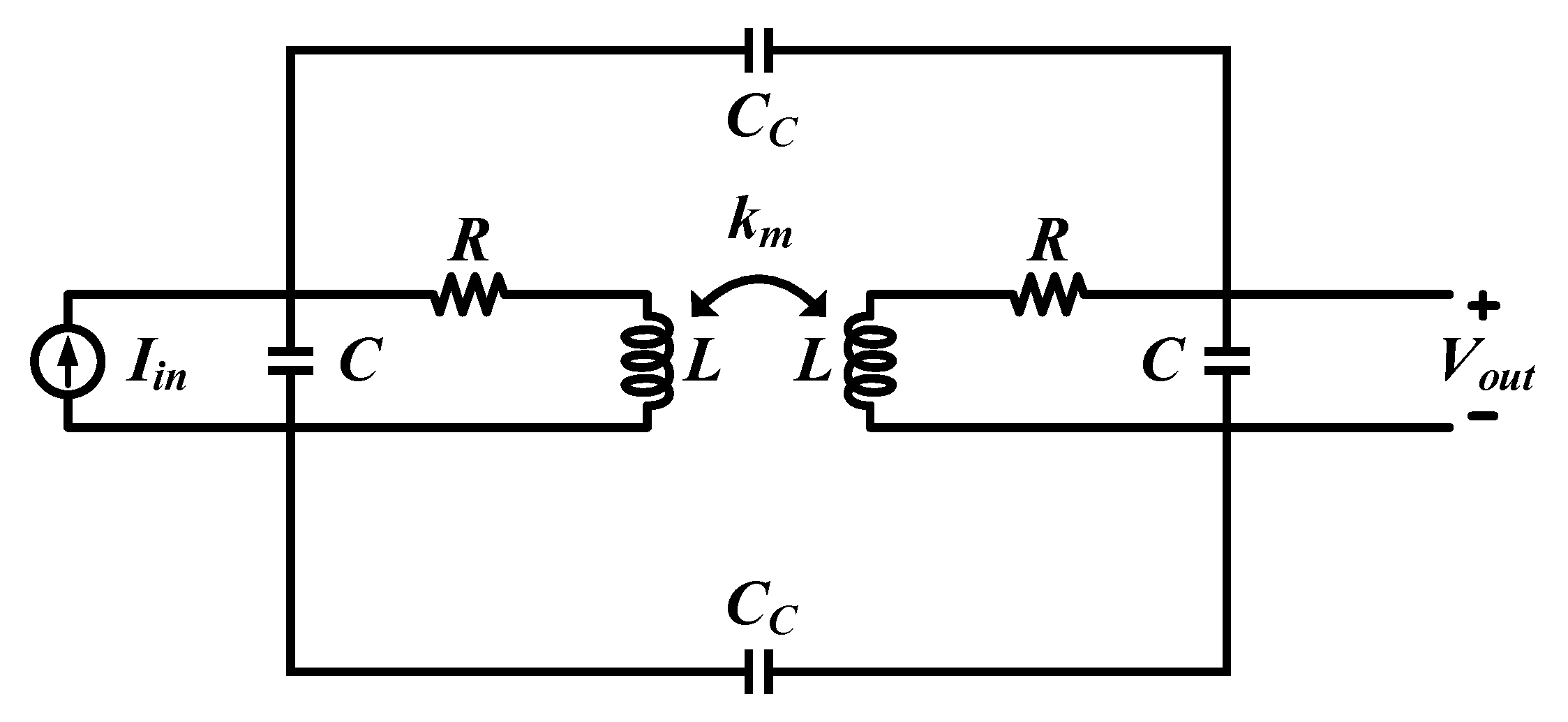
3.2. The Matching Network Analysis and Power Amplifier Driver

Figure 6 is the block diagram of the input buffer circuit and frequency multiplication circuit. The collectors of the SiGe HBTs are connected to the output matching networks, which is convenient for high power heat dissipation. If the collector of SiGe has the square law Q-V characteristic (such as the abrupt junction varactor), the circuit can be set up to allow the second harmonic current to return to the varactor and mix with the fundamental current again. The circuit can make full use of the energy of the second harmonic and improve the efficiency of harmonic frequency doubling. The specific matching circuit is the transformer. For example, in a low-frequency circuit, the transformer is shorted to ground and in terahertz frequency, the harmonics are completely amplified by inductors of the transformer.
To improve the bandwidth of the doublers, transformers are utilized. A transformer is widely used in sub-THz circuits. Its main advantages are as follows. The electromagnetic field of the transformer is very clear, which makes the inductance value of the primary coil and secondary coil and the coupling coefficient have good predictability even at the millimeter wave frequencies. There are three kinds of coupling and tuning mechanisms: magnetic coupling, electrical coupling, and electromagnetic coupling. For each coupling mode, the parameter that is generally concerned is trans-resistance Z, that is, the ratio coefficient of the output voltage to the input current.
The amplitude mismatch of an electromagnetic coupling resonator is related to a single coupling variable k M (magnetic coupling coefficient) or k C (electrical coupling coefficient), Figure 7 shows the model of the magnetic-capacitive coupled resonator (MCCR) which consists of two coupled RLC resonators by mutual inductance M and coupling capacitance Cc. Then the magnetically coupling coefficient is k M = M / L 1 L 2 and the capacitive coupling coefficient is defined as k C = C c / C 1 + C c C 2 + C c . To achieve the widest matching bandwidth, several key parameters need to be co-optimized, such as the resonator frequency ω i = 1 / L i C i + C c and the quality factor Q i = ω i R C i + C c ,   i = 1 , 2 of the two tanks. The input of the BJT (Bipolar Junction Transistor) is a current which will be transferred to a voltage by trans-impedance Z21 of the MCCR network. Thus, the impedance Z21 can indicate the bandwidth of the matching network. Figure 8 shows the calculated Z21 of MCCR with different ω2/ω1 ratios. It can be observed that the widest 3-dB bandwidth amplitudes of Z21 is achieved when the resonant frequencies of the two resonators are close. Based on above analysis, the two pole frequencies ω P 1 ω 0 / 1 k M 1 + k C , ω P 2 ω 0 / 1 + k M 1 k C can be optimized to achieve a bandwidth of 90 GHz.
A stack transformer [22] passive structure is used to implement the MCCR with a very compact area. The pole frequencies of MCCR are determined by the two coupling coefficients kM and kC. They are symmetric and the two factors can be tuned by changing the width of the coupled metal lines. The passive structure with the MCCR 3D EM model is shown in Figure 9, which consists of matching networks for the input buffer, doubler, buffer, doubler, and output buffer. To accurately design the size of the n-p-n transistor, a small signal model of devices is shown in Figure 5 and its key parameters can be calculated from the S-parameter. To realize the maximum output power of the second-harmonic signal, a harmonic impedance matching technique is utilized. Instead of matching the gain of the stage, the sourcepull and loadpull of the transistors are operated to extract the best matching impedance. An improved and complete method for the high-frequency large signal modeling of SiGe HBTs is simulated to gain the optimized impedance for the circuit design. Harmonic impedance matching is utilized for the doubler design because the input matching of the doubler is based on the sourcepull impedance of fundamental frequency and its output matching is based on loadpull impedance of second harmonic frequency.
The MCCR networks are designed in top-metal 1, 2 to reduce the losses and easily control the coupling coefficients kM and kC. The 20-μm n-p-n device using a C-B-E-B-C layout configuration is optimized to reduce the parasitic layout and its ft/fmax is 250/300 GHz when biased at the optimal current density.

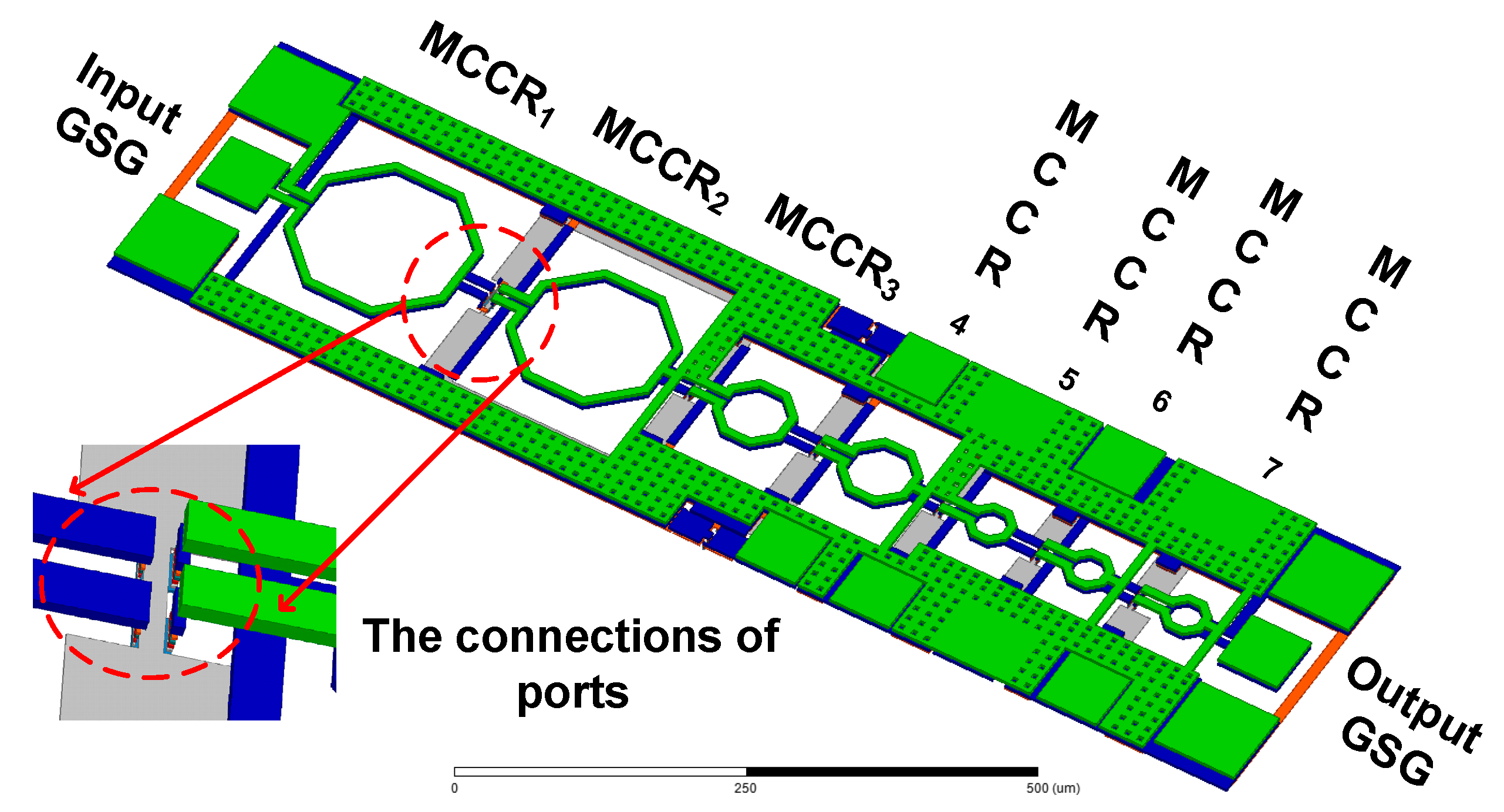
3.3. The Proposed Driver Circuit and QA Circuit

Figure 10 shows the block diagrams of developed broadband FQ. The chains employ similar building blocks, such as the input balun (32.5–55 GHz), input amplifier, inter-stage buffer, output amplifier, and D-band FQ ×4 (130–220 GHz) with wideband frequency doublers ×2. The two PAs are required to drive the frequency doubler with enough power in the operating wideband.
In the first input buffer stage, a broadband buffer has been adopted as the amplifying stage. The instability of the power amplifier is induced by the feedback capacitor Cgd, especially for a relatively low frequency because the SiGe transistors have a large gain at a low frequency. The input balun provides differential signals (32.5–50 GHz), which are fed into the input driver. Adopting the neutralization technique, the Cgd can be reduced and the stability can be improved. A second harmonic amplifier has also been used to improve the desired frequency power and to suppress unwanted harmonics.
The quadrupled signals are further amplified by either broadband PAs to have an output power in the range of 5–9 dBm. The transformer can achieve perfect DC isolation, which greatly simplifies the design of the multi-stage power amplifier. The circuit schematic of the proposed quadrupler is shown in Figure 10 and the measurement diagram of the proposed chip is shown in Figure 11. The second harmonic impedance for Q2a, Q2b and Q4a, Q4b are biased at a low voltage level (0.8–0.9 V), thus the nonlinearity of the transistors is strong, and it can generate large second harmonic signals.
After the second harmonic extracted, the second harmonic signal will be differential by balun. The single-ended doubler employs the device layout where the base and collector are extended lengthwise through the M2-M6 layers before connecting via stacks leading to the MCCR network. Then the MCCR network can realize power matching, dc biasing, and wideband. The emitter, base, and collector resistances and base-emitter and base-collector capacitances can be extracted from the model for small signal matching. Based on these measurement results and theory optimizations, the sizes of the HBT devices and the coupled MCCR can be determined. These sizes of the HBT devices are shown in Table 1.
The conventional ESD (Electro-Static Discharge) protection circuit is mainly composed of diodes, which introduces a large parasitic capacitance to the ground, usually between 0.5–2 pF. This capacitor has a great loss at the millimeter wave frequency, which makes the conventional ESD circuit unable to be used at the millimeter wave frequency. The single to double transformer can well realize ESD protection of a millimeter wave circuit. Based on the above advantages, transformers are widely used in millimeter wave frequency.

4. Measurement Results

The quadrupler signal generator chip has an area of 0.34 mm2 as shown in Figure 12. The circuit was characterized on wafer using a ground signal ground (GSG) probe with a waveguide transition system to VDI mixer. The matching calibration is realized by on-wafer open, short, and through devices. For power calibration, the frequency dependent probes and waveguide losses at the input and output were de-embedded. In the input, a Keysight UXA E9040B analog signal generator with mixers (E8257DV05, 06) provides the input signal from a low frequency up to 220 GHz as shown Figure 13. The power calibration and spectrum measurements are utilized to characterize the fourth harmonic of the proposed quadrupler. The output measurement setup has harmonic mixers (N9029AV05, 06) with a Keysight UXA signal analyzer N5247B spectrum analyzer, which realizes frequency detection up to 220 GHz. The harmonic mixer setup down-converted the RF signal into a single-tone signal and showed it in the spectrum analyzer corresponding to the output frequency of the quadrupler.
At a bias condition of VDD = 1.6 V, Vb1 = 0.85 V, Vb = 0.9 V, the input buffer, quadrupler, and output amplifier draw 10 mA, 6 mA, and 26 mA from the 1.6-V supply, respectively. The output frequencies of 140 GHz and 210 GHz are shown in Figure 14 with output calibration. The phase noise at 156 GHz and 220 GHz is −97 dBc/Hz, which shows the good quality of the output signals as shown in Figure 15.
The output dynamic range of the quadrature defined as the maximum ratio of the largest desired signal to the smallest desired fourth harmonic. In a 130–220-GHz range, the dynamic range of the quadrature signal is above 80 dB and the unwanted harmonic leakage is well below −20 dBc with respect to the fourth harmonic. Figure 16 exhibits the relationship between the input and output power at different frequencies. The output power becomes saturated as the input power increases. The input signal power is from −30 to −5 dBm and the output signal yields an 80-dB dynamic range as illustrated in Figure 16. The maximum gain with buffer is 16 dB with a −15 dBm input at 210 GHz. The phase noise is also measured, and it is increased by 20 dB at 230 GHz with a 1-MHz frequency offset after calibration. At 1.6 V, the presented circuit achieves an efficiency of 3.7% (including all buffers) at 210 GHz. Figure 17 shows the phase noise measurement results for different frequencies.
Table 2 summarizes the performance of the 130–220-GHz frequency quadrupler, and the results are compared with different state-of-the-art frequency quadruplers in paper [19,20,21,22,23,24,25,26,27]. The quadrupler presented in this paper delivers relatively the highest output power and widest bandwidth. Meanwhile, it achieves high gain without using supplementary input drivers. Each passive MCCR network is optimized to achieve the widest bandwidth and the measurement results show that it can achieve a bandwidth that is over 90 GHz and an 80-dB dynamic range, which is the largest among all circuits.
In conclusion, a 130–220-GHz signal generator in a 0.13-μm SiGe technology based on MCCR matching networks and harmonic impedance matching technique is proposed. The MCCR based passive matching networks and the active devices are all analyzed and co-optimized to extend the bandwidth. The measurement results show that the proposed quadrupler provides a 90-GHz bandwidth with an 80-dB dynamic range.

5. Conclusions

This paper presents a broadband FQ fabricated with a standard 130-nm SiGe BiCMOS process. Two broadband push-push frequency doubler (×2) operating at 32.5–55 GHz and 65–110 GHz are employed. To properly drive such doublers, with a sufficient input power and bandwidth, two different power amplifiers (PAs) have been adopted: The former is based on a cascaded configuration and the latter is based on a stacked topology. A nonlinear device model and a systematic methodology to generate maximum power at any desired harmonic is proposed. By manipulating the device nonlinearity and optimizing the embedding networks, optimum conditions for harmonic power generation are provided. A novel broadband signal generator in 0.13-μm silicon-germanium (SiGe) technology with MCCR matching networks and a harmonic impedance matching technique is proposed. The measurement results show that the proposed quadrupler provides a 90-GHz bandwidth with an 80-dB dynamic range and η of 3.7% at 210 GHz. This high-performance frequency FQ can be applied in 6G communication and other sub-THz communication systems.
The efficiency of the current quadrupler is not high enough, which can be improved in the future. Currently, many communication circuit designs are integrated in a CMOS technology [32,33]. The proposed FQ is utilized by a SiGe process, which have a high voltage, and it cannot be integrated with advanced CMOS. Researchers can consider using a CMOS process to complete the relevant design.

Author Contributions

Research methodology, T.W. and S.M.; writing—original draft preparation, S.M., T.W. and Z.C.; supervision, H.Y.; validation, T.W., S.M., L.D. and W.M.; writing—review and editing, S.M., T.W., W.M., J.H. and Z.X. All authors have read and agreed to the published version of the manuscript.

Funding

This work was supported by the National Natural Science Foundation of China (NSFC) (Key Program Grant No. 62034007 and 62104039), the Key-Area Research and Development Program of Guangdong Province (Grant No. 2019B010116002), the Guangdong Basic and Applied Basic Research Foundation (Grant 2019B1515120024), the Shenzhen Science and Technology Program (Grant No. KQTD20200820113051096), the Natural Science Foundation of Shanghai (Grant No. 21ZR1405700), and the Young Scientist Project of MOE Innovation Platform and the Independent Project of State Key Laboratory of ASIC and System (Grant No. 2021MS012).

Data Availability Statement

Data is contained within the article.

Conflicts of Interest

The authors declare no conflict of interest.

Abbreviations

SiGeSilicon-Germanium
FQFrequency Quadrupler
PAPower Amplifier
MCCRMagnetically And Capacitively Coupled Resonator
CMLCurrent Mode Logic
VCOVoltage-Controlled Oscillator
BEOLBack-End-Of-The-Line
EMElectromagnetic
HBTHetero-Junction Bipolar Transistor
ESDElectro-Static Discharge
HFSSHigh Frequency Structure Simulator
RFRadio Frequency
BJTBipolar Junction Transistor
PCPPPhase-Controlled Push-Push
PPPush-Push
CMOSComplementary Metal Oxide Semiconductor

References

  1. Park, J.; Kang, S.; Niknejad, A.M. A 0.38 THz Fully Integrated Transceiver Utilizing a Quadrature Push-Push Harmonic Circuitry in SiGe BiCMOS. IEEE J. Solid-State Circuits 2012, 47, 2344–2354. [Google Scholar] [CrossRef]
  2. Aghasi, H.; Cathelin, A.; Afshari, E. A 0.92-THz SiGe Power Radiator Based on a Nonlinear Theory for Harmonic Generation. IEEE J. Solid-State Circuits 2017, 52, 406–422. [Google Scholar] [CrossRef]
  3. Ng, H.J.; Hasan, R.; Kissinger, D. A Scalable Four-Channel Frequency-Division Multiplexing MIMO Radar Utilizing Single-Sideband Delta–Sigma Modulation. IEEE Trans. Microw. Theory Tech. 2019, 67, 4578–4590. [Google Scholar] [CrossRef]
  4. Ng, H.J.; Kissinger, D. Highly Miniaturized 120-GHz SIMO and MIMO Radar Sensor with On-Chip Folded Dipole An-tennas for Range and Angular Measurements. IEEE Trans. Microw. Theory Tech. 2018, 66, 2592–2603. [Google Scholar] [CrossRef]
  5. Centurelli, F.; Monsurrò, P.; Scotti, G.; Tommasino, P.; Trifiletti, A. A Power Efficient Frequency Divider with 55 GHz Self-Oscillating Frequency in SiGe BiCMOS. Electronics 2020, 9, 1968. [Google Scholar] [CrossRef]
  6. Silva Valdecasa, G.; Altabas, J.A.; Kupska, M.; Jensen, J.B.; Johansen, T.K. A 5–50 GHz SiGe BiCMOS Linear Transimpedance Amplifier with 68 dBΩ Differential Gain towards Highly Integrated Quasi-Coherent Receivers. Electronics 2021, 10, 2349. [Google Scholar] [CrossRef]
  7. Chen, Z.; Hou, D.; Chen, J.-X.; Yan, P.; Bao, L.; Hong, Z.; Zheng, Y. A K-Band FMCW Frequency Synthesizer Using Q-Boosted Switched Inductor VCO in SiGe BiCMOS for 77 GHz Radar Applications. Electronics 2020, 9, 1933. [Google Scholar] [CrossRef]
  8. Men, K.; Liu, H.; Yeo, K.S. Design of a Ka-Band U-Shaped Bandpass Filter with 20-GHz Bandwidth in 0.13-μm BiCMOS Technology. Electronics 2020, 9, 1608. [Google Scholar] [CrossRef]
  9. Coen, C.T.; Frounchi, M.; Lourenco, N.E.; Cheon, C.D.Y.; Williams, W.L.; Cressler, J.D. A 60-GHz SiGe Radiometer Calibration Switch Utilizing a Coupled Avalanche Noise Source. IEEE Microw. Wirel. Compon. Lett. 2020, 30, 417–420. [Google Scholar] [CrossRef]
  10. Han, J.; Jiang, Y.; Guo, G.; Cheng, X. A Reconfigurable Analog Baseband Circuitry for LFMCW RADAR Receivers in 130-nm SiGe BiCMOS Process. Electronics 2020, 9, 831. [Google Scholar] [CrossRef]
  11. Kibaroglu, K.; Sayginer, M.; Rebeiz, G.M. A 28 GHz transceiver chip for 5G beamforming data links in SiGe BiCMOS. In Proceedings of the 2017 IEEE Bipolar/BiCMOS Circuits and Technology Meeting (BCTM), Miami, FL, USA, 19–21 October 2017; pp. 74–77. [Google Scholar] [CrossRef]
  12. Grzyb, J.; Heinemann, B.; Pfeiffer, U.R. Solid-State Terahertz Superresolution Imaging Device in 130-nm SiGe BiCMOS Technology. IEEE Trans. Microw. Theory Tech. 2017, 65, 4357–4372. [Google Scholar] [CrossRef]
  13. Chung, W.; Kim, C.; Kim, S.S.; Hong, S. Design of 94-GHz Highly Efficient Frequency Octupler Using 47-GHz Current-Reusing Class-C Frequency Quadrupler. IEEE Trans. Microw. Theory Tech. 2020, 68, 775–784. [Google Scholar] [CrossRef]
  14. Golcuk, F.; Gurbuz, O.D.; Rebeiz, G.M. A 0.39–0.44 THz 2x4 Amplifier-Quadrupler Array with Peak EIRP of 3–4 dBm. IEEE Trans. Microw. Theory Tech. 2013, 61, 4483–4491. [Google Scholar] [CrossRef]
  15. Wu, L.; Liao, S.; Xue, Q. A 312-GHz CMOS Injection-Locked Radiator with Chip-and-Package Distributed Antenna. IEEE J. Solid-State Circuits 2017, 52, 2920–2933. [Google Scholar] [CrossRef]
  16. Yang, Y.; Gurbuz, O.D.; Rebeiz, G.M. An Eight-Element 370–410-GHz Phased-Array Transmitter in 45-nm CMOS SOI with Peak EIRP of 8–8.5 dBm. IEEE Trans. Microw. Theory Tech. 2016, 64, 4241–4249. [Google Scholar] [CrossRef]
  17. Cao, T.; Liu, Y.J.; Jiang, J.; Zhang, Q.; Lin, C.; Yang, D.; Zhang, G.; Yang, C.; Zhou, J. Frequency Multiplier-Based Millimeter-Wave Vector Signal Transmitter Using Digital Predistortion with Constrained Feedback Bandwidth. IEEE Trans. Microw. Theory Tech. 2020, 68, 1819–1829. [Google Scholar] [CrossRef]
  18. Jaffri, I.; Ayed, A.B.; Darwish, A.M.; Mitran, P.; Boumaiza, S. Novel Baseband Equivalent Model for Digital Predistortion of Wideband Frequency-Multiplier-Based Millimeter Wave Sources. IEEE Trans. Microw. Theory Tech. 2020, 68, 3942–3957. [Google Scholar] [CrossRef]
  19. Bousnina, S.; Mandeville, P.; Kouki, A.B.; Surridge, R.; Ghannouchi, F.M. Direct parameter-extraction method for HBT small-signal model. IEEE Trans. Microw. Theory Tech. 2002, 50, 529–536. [Google Scholar] [CrossRef]
  20. Kim, W.; Kang, S.; Lee, K.; Chung, M.; Kang, J.; Kim, B. Analysis of nonlinear behavior of power HBTs. IEEE Trans. Microw. Theory Tech. 2002, 50, 1714–1722. [Google Scholar]
  21. Sheinman, B.; Wasige, E.; Rudolph, M.; Doerner, R.; Sidorov, V.; Cohen, S.; Ritter, D. A peeling algorithm for extraction of the HBT small-signal equivalent circuit. IEEE Trans. Microw. Theory Tech. 2002, 50, 2804–2810. [Google Scholar] [CrossRef]
  22. Li, S.; Huang, M.; Jung, D.; Huang, T.; Wang, H. A 28 GHz Current-Mode Inverse-Outphasing Transmitter Achieving 40%/31% PA Efficiency at Psat/6 dB PBO and Supporting 15 Gbit/s 64-QAM for 5G Communication. In Proceedings of the 2020 IEEE International Solid-State Circuits Conference (ISSCC), San Francisco, CA, USA, 16–20 February 2020; pp. 365–368. [Google Scholar]
  23. Huang, D.; LaRocca, T.R.; Samoska, L.; Fung, A.; Chang, M.F. 324 GHz CMOS Frequency Generator Using Linear Superposition Technique. In Proceedings of the 2008 IEEE International Solid-State Circuits Conference, San Francisco, CA, USA, 3–7 February 2008; pp. 476–629. [Google Scholar]
  24. Wang, Y.; Goh, W.L.; Xiong, Y. A 9% power efficiency 121-to-137 GHz phase-controlled push-push frequency quadrupler in 0.13μm SiGe BiCMOS. In Proceedings of the 2012 IEEE International Solid-State Circuits Conference, San Francisco, CA, USA, 19–23 February 2012; pp. 262–264. [Google Scholar]
  25. Ku, B.; Chung, H.; Rebeiz, G.M. A Milliwatt-Level 70–110 GHz Frequency Quadrupler with >30 dBc Harmonic Rejection. IEEE Trans. Microw. Theory Tech. 2018, 68, 1697–1705. [Google Scholar] [CrossRef]
  26. Kucharski, M.; Eissa, M.H.; Malignaggi, A.; Wang, D.; Ng, H.J.; Kissinger, D. D-Band Frequency Quadruplers in BiCMOS Technology. IEEE J. Solid-State Circuits 2018, 53, 2465–2478. [Google Scholar] [CrossRef]
  27. Wu, K.; Mansha, M.W.; Hella, M. A 99–132 GHz Frequency Quadrupler with 8.5 dBm Peak Output Power and 8.8% DC-to-RF Efficiency in 130 nm BiCMOS. In Proceedings of the 2020 IEEE/MTT-S International Microwave Symposium (IMS), Los Angeles, CA, USA, 4–6 August 2020; pp. 476–479. [Google Scholar]
  28. Steinweg, L.; Rieß, V.; Stärke, P.; Testa, P.V.; Carta, C.; Ellinger, F. A Low-Power 255-GHz Single-Stage Frequency Quadrupler in 130-nm SiGe BiCMOS. IEEE Microw. Wirel. Compon. Lett. 2020, 30, 1101–1104. [Google Scholar] [CrossRef]
  29. Stärke, P.; Rieß, V.; Carta, C.; Ellinger, F. Frequency Multiplier-by-4 (Quadrupler) with 52 dB Spurious-Free Dynamic Range for 152 GHz to 220 GHz (G-Band) in 130 nm SiGe. In Proceedings of the 2020 IEEE Radio Frequency Integrated Circuits Symposium (RFIC), Los Angeles, CA, USA, 4–6 August 2020; pp. 251–254. [Google Scholar]
  30. Ali, A.; Yun, J.; Ng, H.J.; Kissinger, D.; Giannini, F.; Colantonio, P. Wideband Frequency Quadrupler for D-Band Applications in BiCMOS Technology. In Proceedings of the 2020 23rd International Microwave and Radar Conference (MIKON), Warsaw, Poland, 5–8 October 2020; pp. 229–231. [Google Scholar]
  31. Jamal, F.I.; Eissa, M.H.; Borngräber, J.; Ng, H.J.; Kissinger, D.; Wessel, J. A low-power 190–255 GHz frequency quadrupler in SiGe BiCMOS technology for on-chip spectroscopic applications. In Proceedings of the 2017 IEEE Radio and Wireless Symposium (RWS), Phoenix, AZ, USA, 15–18 January 2017; pp. 94–97. [Google Scholar]
  32. Liang, Y.; Boon, C.C.; Zhang, H.; Tang, X.; Zhang, Q.; Yu, H. A 13.5-Gb/s 140-GHz Silicon Redriver Exploiting Metadevices for Short-Range OOK Communications. IEEE Trans. Microw. Theory Tech. 2020, 1, 239–253. [Google Scholar] [CrossRef]
  33. Ma, S.; Lin, J.; Ma, C.; Yu, H. A 140 GHz Transceiver for 4 × 4 Beamforming Short-Range Communication in 65 nm CMOS. In Proceedings of the 2019 IEEE Asia-Pacific Microwave Conference (APMC), Singapore, 10–13 December 2019; pp. 1613–1615. [Google Scholar]
Figure 1. Back-end-of-the-line (BEOL) cross section of the 130-nm SiGe BiCMOS technology.
Electronics 11 00825 g001
Figure 2. The connection between the active device and the passive device.
Electronics 11 00825 g002
Figure 3. Device model of the HBTs (Heterojunction Bipolar Transistors).
Electronics 11 00825 g003
Figure 4. Junction capacitance curve with nonlinearity.
Electronics 11 00825 g004
Figure 5. The collectors of the two HBTs devices are connected to form nonlinear capacitors by the differential voltage source.
Electronics 11 00825 g005
Figure 6. (a) Block diagram of the input buffer circuit. (b) Block diagram of the frequency multiplication circuit.
Electronics 11 00825 g006
Figure 7. Model of electromagnetic coupling and the capacitively coupling transformer.
Electronics 11 00825 g007
Figure 8. Calculated Z21 of MCCR (Magnetically and Capacitively Coupled Resonator) with different ω2/ω1 ratios.
Electronics 11 00825 g008
Figure 9. Passive structure with MCCR 3D EM model. (GSG: Ground-Signal-Ground).
Electronics 11 00825 g009
Figure 10. The block diagrams of developed broadband FQ (Frequency Quadrupler).
Electronics 11 00825 g010
Figure 11. The measurement diagram of the proposed chip.
Electronics 11 00825 g011
Figure 12. Die micrograph of the developed FQ chip and size of the devices.
Electronics 11 00825 g012
Figure 13. The measurement setup.
Electronics 11 00825 g013
Figure 14. The output spectrum of the proposed chip (a) 140 GHz and (b) 210 GHz.
Electronics 11 00825 g014
Figure 15. The output phase noise of signals (a) 156 GHz and (b) 220 GHz.
Electronics 11 00825 g015
Figure 16. The output power at different frequencies.
Electronics 11 00825 g016
Figure 17. The phase noise measurement results for different frequencies.
Electronics 11 00825 g017
Table 1. The sizes of the HBT devices.
Stage of n-p-nSize of n-p-n Transistor
MEmitter Width (nm)—70
16Emitter Length (nm)—900
26STI (nm)—440
34baspolyx (nm)—300
44bipwinx (nm)—70
54bipwiny (nm)—100
64empolyx (nm)—150
empolyy (nm)—180
Active transistors design for quadrature
Table 2. The comparison with other papers.
ReferenceMethodTechnologyFreq. (GHz)NGain (dB)Pout (dBm)PDC (mW)Input BuffersOutput Buffersη (%)
[23]LS90 nm CMOS a322–3264N−4612NN0.0002
[24]PCPP b0.13 μm SiGe121–137×40.6−2.435.2 YN1.6
[25]Cascaded Doubler0.12 μm SiGe70–110×4−4.5−4.5240 NN0.3–0.8
[26]Injection-locked 0.13 μm SiGe148–183×45−449NN0.8
[27]Cascaded Doubler0.13 μm SiGe99–132×4N8.579.2NN8.8
[28]PCPP b0.13 μm SiGe248–262×4N−8.422.4NN0.65
[29]PP c0.13 μm SiGe152–220×4N−145NY1.8
[30]Cascaded Doubler0.13 μm SiGe100–184×4255@13042NN7.5
[31]PP0.13 μm SiGe190–255×4−24.4−16.448NN0.048
This workMCCR + HIM0.13 μm SiGe130–220×4161.86@210
GHz
42YY3.7@210 GHz
a. CMOS: Complementary Metal Oxide Semiconductor. b. PCPP: Phase-Controlled Push-Push. c. PP: Push-Push
Publisher’s Note: MDPI stays neutral with regard to jurisdictional claims in published maps and institutional affiliations.

