Abstract
In this paper, a novel switching scheme using discontinuous pulse-width modulation (DPWM) for a zero-voltage switching (ZVS) grid-connected three-phase inverter is proposed. ZVS in the main and auxiliary switches was achieved. Moreover, the reverse recovery currents of the anti-parallel diodes in the main switches were suppressed. A circuit analysis was performed, and a simulation was carried out. Furthermore, a prototype of the ZVS grid-connected three-phase inverter was constructed to verify the effectiveness of the proposed PWM control scheme. Both the simulation and experimental results verified the validity of the proposed PWM control scheme.
1. Introduction
Three-phase inverters are widely utilized in PV systems, wind power generation, electrical vehicles, and uninterruptible power systems, etc. Especially, distributed grid-connected inverters play an important role in renewable energy generation systems as the interface between the renewable energy and the grid. The conventional six-switch three-phase inverter is a preferred topology with several advantages such as lower current stress and higher efficiency. However, the anti-parallel diodes of the six switches have a reverse recovery problem that causes many switching loss and electromagnetic interference problems.
Over the past few years, various soft-switching techniques for three-phase inverters have been studied [1,2,3,4,5,6,7,8,9,10,11,12]. Generally, the voltage of the DC link is periodically resonated to a zero voltage level to create soft-switching conditions, which causes the three-phase six switches achieve zero-voltage switching at the corresponding time. The typical method to achieve ZVS is by adding an auxiliary resonant circuit in the inverter [2]. According to the different locations of the auxiliary circuit, the soft-switching method of DC–AC voltage-source inverters can be classified into two categories: DC-side auxiliary circuit topologies [1,2,3,4,5,6,7] and AC-side auxiliary circuit topologies [8,9,10,11]. In DC-side auxiliary circuit topologies, an auxiliary circuit is inserted between the DC voltage source and the main six-switch bridge to achieve the zero-voltage condition. Generally speaking, according to the clamp capacitor location, the clamp capacitor can be in series with resonant inductance [1,2] or in series with the auxiliary switch [3,4,5,6,7] to achieve ZVS. If the clamp capacitor is in series with the auxiliary switch, the reverse recovery current of the anti-parallel diodes can be easily suppressed, but the switch voltage stress is high. If the clamp capacitor is in series with the resonant inductor, the switch voltage stress is equal to the DC link voltage. In addition, different PWM strategies for ZVS have been developed. The space-vector pulse-width modulation (SVPWM) control strategy has been utilized for ZVS in the literature [1,2,3,7], and the discontinuous pulse-width modulation (DPWM) control strategy has also been studied to achieve ZVS in the literature [12,13]. However, although there is no additional component added in the circuit [12], the inverter-side current is larger and the current stress on the main switches is higher than that in the literature [1,2,3,4,5,6,7]. In addition, the filter design is more complicated due to the variable switching frequency operation. In [13], in order to unify the PWM methods for soft-switching active-clamping three-phase power converters, the edge-aligned PWM (EA-PWM) was proposed to simplify the control method. Nevertheless, the EA-PWM needs three-phase current sensors to obtain information on the filter’s current polarities to achieve ZVS in the active switches. Moreover, the soft-switching condition is affected by the modulation index, which may reduce the ability to achieve ZVS in any modulation index.
In the DPWM control strategy, only two of three legs are switching at any time. Therefore, the switching loss and electromagnetic interference (EMI) can be reduced. In order to reduce the switching loss, in this paper, a carrier-based ZVS DPWM (CB-DPWM) control strategy was studied for grid-connected three-phase inverters. A simple saw-tooth carrier waveform with positive and negative slope rates was developed to achieve ZVS in both the main and auxiliary switches. Using this method, the auxiliary switch, , control signal can be generated more easily compared with the literature [1,2]. In addition, the ZVS of the main and auxiliary switches can be obtained. Moreover, the reverse recovery current of the anti-parallel diodes in the main switches can also be reduced in the proposed modulation scheme. Furthermore, the voltage stress of main and the auxiliary switches was still equal to DC bus voltage.
The remaining contents of this paper are organized as follows. First, the circuit configuration and the operating principle of the proposed ZVS DPWM control strategy are described in Section 2 and Section 3. Based on the proposed ZVS DPWM control strategy, simulation and experimental results are offered in Section 4 to verify the validity of the proposed control strategy for a ZVS grid-connected three-phase six-switch inverter. Finally, some conclusions are offered in Section 5.
2. Proposed Modulation Scheme
The circuit of the ZVS inverter is shown in Figure 1 [1,2]. The circuit topology is composed of a standard six-switch grid-connected inverter and an auxiliary resonant circuit that is connected with the distributed energy resources (DERs) in the DC side. In the auxiliary circuit, the auxiliary switch, , is conducted most of the time during the switching period. While the auxiliary switch, , is turned ON, the resonant inductor, , is charged. While the auxiliary switch, , is turned OFF, the energy stored in the resonant inductor, , releases energy to the parasitic capacitors of the main switches. When the auxiliary switch, S7, is switched once in a PWM period, both the main and auxiliary switches can achieve ZVS. In addition, the reverse recovery current of the main switches can be suppressed. Thus, the system’s conversion efficiency can be increased.
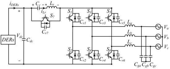
Figure 1.
The circuit topology of the ZVS grid-connected inverter.
The proposed DPWM control strategy and corresponding carrier waveform are shown in Figure 2. In order to achieve zero-voltage switching and decrease the switching numbers of the main and auxiliary switches, a ZVS carrier-based PWM is proposed to reduce switching loss and improve energy conversion efficiency. The proposed control strategy judges three-phase DPWM control signals to determine the slope of the saw-tooth carrier waveform. When one of the three-phase DPWM control signals reaches high level (i.e., /2), the slope of the saw-tooth waveform is negative, and when one of the three-phase DPWM control signals reaches low level (i.e., /2), the slope of the saw-tooth carrier waveform is positive.
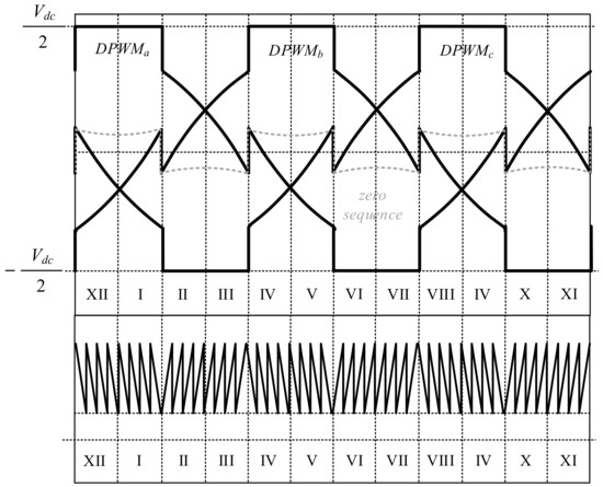
Figure 2.
Proposed DPWM method and carrier waveform diagram.
In the proposed control scheme, the zero vectors, and , were selected as shown in Figure 3, and the auxiliary switch, , control signal is determined to achieve ZVS in the main – and switches. The generation of the signal is mainly based on the dead-time among the three legs in the three-phase inverter as shown in Figure 4. Take sector I and sector II as an example. In the control signal in sector I, one of the three-phase DPWM control signals reaches high level, i.e., DPWMa. Then, the negative slope of the saw-tooth waveform is utilized, and the control signals are generated as shown in Figure 4a. In the meantime, the zero vector, , is naturally selected. If the dead-time of any two legs occur at the same time, the control signal is established. In the same manner, the corresponding control signals in sector II are shown in Figure 4b, and the positive slope of the saw-tooth waveform is utilized, the zero vector, , is naturally selected, and control signal is also established.
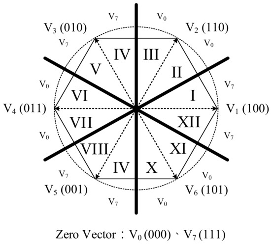
Figure 3.
Sectors of the space-vector diagram.
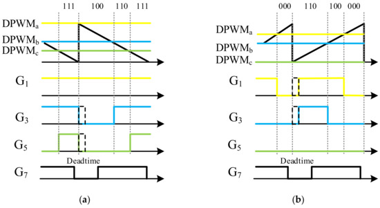
Figure 4.
The proposed DPWM scheme: (a) sector I; (b) sector II.
3. Analysis of DPWM Grid-Connected Inverter
According to the proposed DPWM method and the zero vector selection in Figure 2, Figure 3 and Figure 4, there are twelve sectors in a line-cycle period. The twelve-sector modulation can be operated in sequence. Take sector I as an example and assume a three-phase current: . For a convenient explanation of how the proposed modulation scheme works, the following assumptions were made to simplify the analysis of the grid-connected ZVS inverter;
- (1)
- The main switches, –, and auxiliary switch, , were considered to be ideal switches connected with corresponding anti-parallel diodes;
- (2)
- All of the parasitic capacitances, –, paralleled the switches –, respectively;
- (3)
- In this architecture, the current ripple of and in grid-side inductor was small, and and were considered as constant current sources in a switching period;
- (4)
- The capacitance of the clamping capacitor, , was so large that the voltage ripple across it was relatively small; thus, can be regarded as a voltage source;
- (5)
- The resonant frequency of and was much lower than the operation frequency of the inverter. In this paper, the filter resonant frequency was 707 Hz, and the operation switching frequency was 18 kHz;
- (6)
- In order to explain the reverse recovery current of switch body diode, icex, x ∈ {1, 2, …, 7} denotes the switch current including the parasitic capacitor current, and isx, x ∈ {1, 2, …, 7} denotes the switch current except the parasitic capacitor current.
The circuit operation, equivalent circuit, and theoretical waveform are illustrated in Figure 5, Figure 6 and Figure 7, respectively. The following are the working stages of the proposed ZVS DPWM control strategy for grid-connected three-phase inverters.
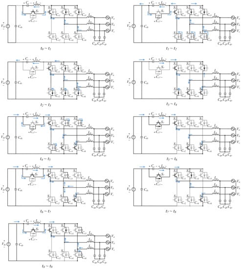
Figure 5.
The operation stages of the proposed ZVS DPWM control strategy in sector I.
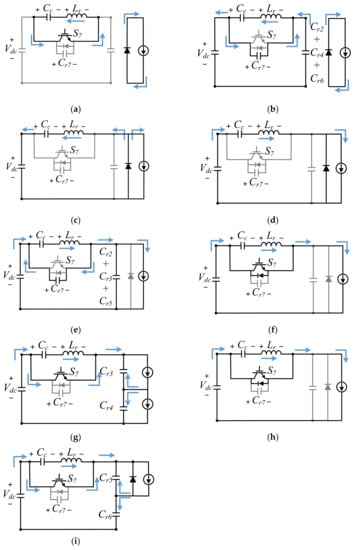
Figure 6.
The equivalent circuits of the operation stages of the proposed ZVS grid-connected inverter. (a) t0~t1. (b) t1~t2. (c) t2~t3. (d) t3~t4. (e) t4~t5. (f) t5~t6. (g) t6~t7. (h) t7~t8. (i) t8~t9.
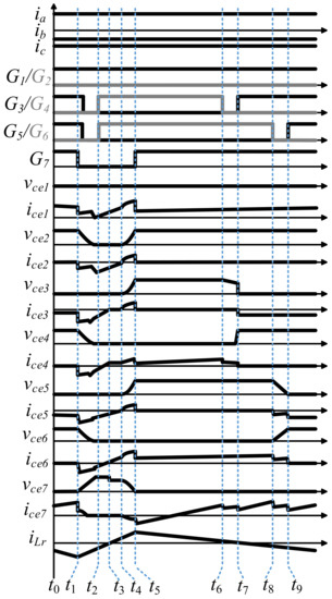
Figure 7.
The theoretical waveform of the proposed ZVS DPWM control strategy.
State 1 ():
The circuit is operated at vector state 111. The main switch, , auxiliary switch, , and the anti-parallel diodes, and , are ON. The inverter is operated at zero vector. The resonant inductor, , is charged by the clamping voltage,. The equivalent circuit is shown in Figure 6a, and the relationship between and is obtained as follows:
State 2 ():
The resonant inductor, , resonates with and . The auxiliary switch, , is turned OFF at under the ZVS condition due to the resonance where is discharging and is charging in this moment. During this state, switches S3 and S5 are turned OFF. The energy stored in inductor, , is returned to the DC capacitor. The equivalent circuit is shown in Figure 6b, and the relationship between, , and is expressed as follows:
State 3 ():
At this time, the circuit is operated at vector state 100. The voltages of are discharged to zero, and the voltage of is charged to The anti-parallel diodes are ON. The switches S4 and S6 are turned ON under ZVS conditions at instant time t2, and the resonant inductor, , suppresses the reverse recovery current of the anti-parallel diode, . The equivalent circuit is shown in Figure 6c, and the relationship between and is derived as follows:
State 4 ():
The main switches , , and remain ON, and the resonant inductor, , suppresses the reverse recovery current of the anti-parallel diodes, and . The power flows from the DC side to the AC side. The equivalent circuit is shown in Figure 6d, and the relationship between and is expressed as follows:
State 5 ():
The resonant inductor, , resonates with , and the anti-parallel diode, , is ready to be turned ON. During this state, are charged, and is discharged. The power still flows from the DC side to the AC side. The equivalent circuit is shown in Figure 6e, and the relationship between the voltage and current can be obtained as follows:
State 6 ():
At this state, the circuit is still operated at vector state 100, and the main switches,, , and , are ON. The auxiliary switch, , is turned ON under the ZVS condition. The voltage of the clamping capacitor, , is charged by the resonant inductor current, , and the power flows from the DC side to the AC side. The equivalent circuit is shown in Figure 6f, and the relationship between and is as follows:
State 7 ():
At this state, the circuit is operated at vector state 100. The phase current discharges voltage and charges voltage . The main switch, , is turned OFF under the ZVS condition, and the power flows from the DC side to the AC side. The equivalent circuit is shown in Figure 6g, and the relationship between the voltage and current can be derived as follows:
State 8 ():
At this state, the circuit is operated at vector state 110. The main switches, and , the auxiliary switch, , and the anti-parallel diode, , are in the conducting state. The power flows from the DC side to the AC side. The equivalent circuit is shown in Figure 6h, and the relationship between and is expressed as follows:
State 9 ():
At this state, the circuit is still operated at vector state 110. The phase current discharges voltage and charges voltage . The main switch, , is turned OFF under the ZVS condition, and the power flows from the DC side to the AC side. The equivalent circuit is shown in Figure 6i. After this stage, the circuit operation returns to the first stage and starts a new cycle. The relationship between the voltage and current can be obtained as follows:
4. Simulation and Experimental Results
After the explanation of the theoretical analysis of the proposed ZVS PWM control scheme, the simulation and experiment were carried out to verify the validity the proposed ZVS PWM control scheme. Hence, the system parameters of the grid-connected ZVS inverter are listed in Table 1 for the simulation and experiment.

Table 1.
System parameters for the simulation and experiment.
The system control block of the grid-connected ZVS inverter is shown in Figure 8. The grid voltage and inverter output current were sensed and fed into the controller. The three-phase voltages and currents were transferred from nature reference frame to the synchronous reference frame. There exist three control loops in the proposed system. The first, second, and third control loops were the droop control, voltage control, and current control, respectively, as shown in Figure 8. The ZVS voltage source inverter was operated at a grid-supporting condition. In this paper, a 3 kW system was constructed for the simulation and experiment to verify the validity of the proposed ZVS PWM control scheme. The software PSIM version 9.1 was adopted for the simulation. In the experiment, the adopted active switches, , were with an insulated-gate bipolar transistor (Fuji 2MBI100VA-060-50) that had a parasitic capacitor of 2 nF. The system controller was realized using DSP (TMS320F28335) manufactured by Texas Instruments and FPGA (Cmod-A7-35T) manufactured by Digilent, Inc. The design parameters of the circuit are listed in Table 1.
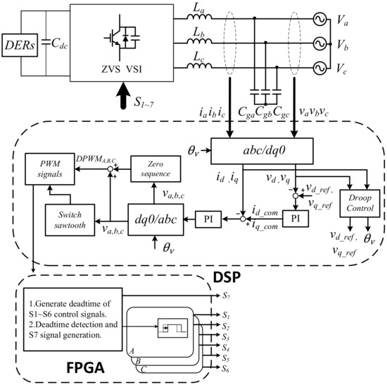
Figure 8.
The control block of the proposed ZVS DPWM control strategy for grid-connected three-phase inverters.
Figure 9a,b show the simulation and experimental results of grid-connected voltage , , and output phase current respectively. As can be observed from Figure 9, inverter output current is phase shifted by 180 degrees from grid-connected voltage . That means the power flows from the DC side to grid side.
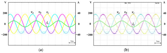
Figure 9.
(a) Simulation waveforms and (b) experimental waveforms of the grid voltages , , and and output phase current .
The simulation and experimental waveforms of the voltage, , and current, of the main switch, , operated in sector I are shown in Figure 10a,b, respectively. As can be observed form Figure 10, the ZVS ON was achieved in the switch and, at this time, the reverse recovery current in body diode of switch S3 was suppressed as shown in Figure 11a,b for the simulation and experimental results, respectively. As can be seen from the simulation in Figure 11a, the current iS3, which flowed through the body diode of switch S3, was successfully suppressed when the switch S3 was turned OFF. It should be noticed that in Figure 11b, the measured waveform can only show the current ice3, which is the total current flowing through the switch and the parasitic capacitor. The simulation and experimental waveforms of voltage and current of the are shown in Figure 12a,b, respectively. It follows from Figure 12 that ZVS ON was indeed achieved in the . The simulation and experimental waveforms of the and the in the auxiliary circuit are shown in Figure 13a,b, respectively. The was at a low voltage level, and was magnetized and demagnetized via control by the S7. From Figure 9, Figure 10, Figure 11, Figure 12 and Figure 13, one can see that the simulation and experimental results were in close agreement. The ZVS in both the main and auxiliary switches were indeed achieved. In addition, the reverse recovery current of the main switches was suppressed in the proposed ZVS DPWM control strategy.
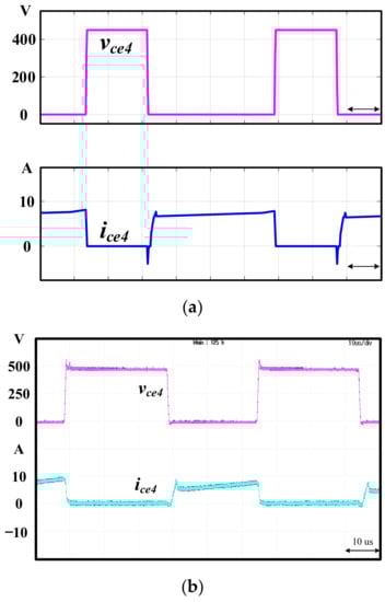
Figure 10.
(a) Simulation waveforms and (b) experimental waveforms of the voltage and current of switch .
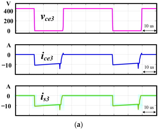
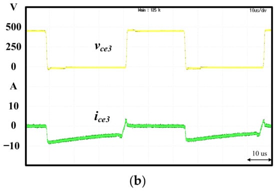
Figure 11.
(a) Simulation waveforms of , , and ; (b) the experimental waveforms of and .
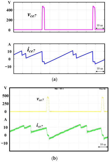
Figure 12.
(a) Simulation waveforms and (b) experimental waveforms of the voltage and current of .
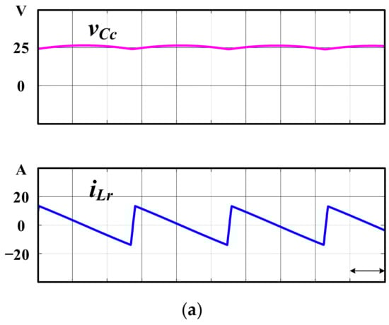
Figure 13.
(a) Simulation waveforms and (b) experimental waveforms of and .
The conversion efficiency of the implementation is shown in Figure 14 in the comparison between the traditional sinusoidal pulse-width modulation (SPWM) without auxiliary circuit and the proposed ZVS DPWM control scheme. From a light load to a full load, the proposed ZVS DPWM control scheme had higher efficiency than the SPWM operation. The efficiency was significantly improved and reached a conversion efficiency of 97.1% at a load of 3 kW.
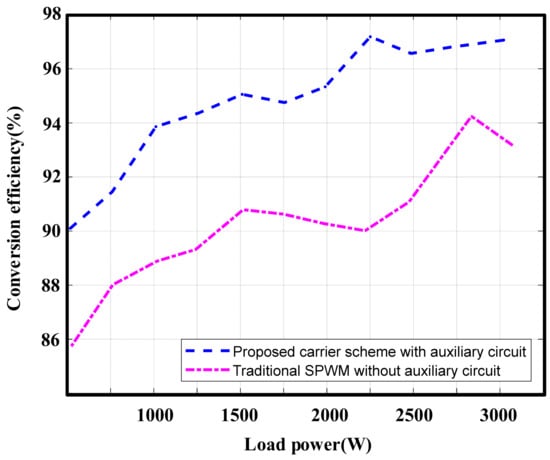
Figure 14.
Efficiency comparison between the proposed ZVS PWM control scheme and the traditional SPWM control scheme.
Finally, to further reveal the potential merits of the proposed PWM control scheme, Table 2 is provided to summarize the comparisons of the extra elements, soft switching range, switching frequency, control complexity, switch voltage stress, and current stress as well as the filter design of the literature [2,3,12,13] and the proposed PWM control scheme.
Table 2.
Comparison of the different ZVS methods for inverters.
5. Conclusions
In this article, a ZVS DPWM strategy for a grid-connected three-phase inverter was proposed. The saw-tooth carrier waveform with positive and negative slopes was utilized to generate the control signal of , and it achieved ZVS in both the main and auxiliary switches. In addition, the reverse recovery current in the anti-parallel diodes of the main switches were suppressed. The circuit operation was clearly explained. Finally, a prototype was constructed. Both the simulation and experimental results verified the validity of the proposed ZVS DPWM strategy for the grid-connected three-phase inverter.
Author Contributions
Conceptualization, Y.-H.L.; Methodology, J.-Y.C.; Validation, Y.Z. The paper was a collaborative effort among the authors. The authors contributed collectively to the theoretical analysis, modeling, simulation, experiment, and manuscript preparation. All authors have read and agreed to the published version of the manuscript.
Funding
This research was funded by [the Ministry of Science and Technology of R.O.C] grant number [110-3116-F-008-001].
Institutional Review Board Statement
Not applicable.
Informed Consent Statement
Not applicable.
Data Availability Statement
Not applicable.
Acknowledgments
This work was supported by the Ministry of Science and Technology of R.O.C under Grant MOST 110-3116-F-008-001.
Conflicts of Interest
The authors declare no conflict of interest.
References
- Li, R.; Ma, K.; Xu, D. A Novel Minimum Voltage Active Clamping SVM (MVAC-SVM) Controlled Three-Phase PFC. In Proceedings of the Twenty-Fourth Annual IEEE Applied Power Electronics Conference and Exposition, Washington, DC, USA, 15–19 February 2009; pp. 1879–1885. [Google Scholar]
- Li, R.; Ma, Z.; Xu, D. A ZVS Grid-Connected Three-Phase Inverter. IEEE Trans. Power Electron. 2012, 27, 3595–3604. [Google Scholar] [CrossRef]
- Li, R.; Xu, D. A zero-voltage switching three-phase inverter. IEEE Trans. Power Electron. 2014, 29, 1200–1210. [Google Scholar]
- Du, C.; Hurley, W.G.; Xu, D. Design Methodology of Resonant Inductor in a ZVS Inverter. IEEE J. Emerg. Sel. Top. Power Electron. 2015, 3, 1142–1150. [Google Scholar] [CrossRef]
- Du, C.; Xu, D.; He, N.; Zhu, N. Modeling and Optimization of a Zero-Voltage Switching Inverter for High Efficiency and Miniaturization. IEEE Trans. Power Electron. 2017, 32, 150–163. [Google Scholar] [CrossRef]
- Du, C.; He, N.; Xu, D. Design of zero-voltage-switching three-phase grid inverter. In Proceedings of the IEEE 2nd Annual Southern Power Electronics Conference (SPEC), Auckland, New Zealand, 5–8 December 2016; pp. 1–6. [Google Scholar]
- Wu, Y.; He, N.; Chen, M.; Xu, D. Generalized Space-Vector-Modulation Method for Soft-Switching Three-Phase Inverters. IEEE Trans. Power Electron. 2021, 36, 6030–6045. [Google Scholar] [CrossRef]
- De Doncker, R.W.; Lyons, J.P. The auxiliary resonant commutated pole converter. In Proceedings of the Conference Record of the 1990 IEEE Industry Applications Society Annual Meeting, Seattle, WA, USA, 7–12 October 1990; pp. 1228–1235. [Google Scholar]
- Beukes, H.J.; Enslin, J.H.R.; Spee, R. Performance of the auxiliary resonant commutated pole converter in converter based utility devices. In Proceedings of the PESC Record 27th Annual IEEE Power Electronics Specialists Conference, Baveno, Italy, 23–27 June 1996; pp. 1033–1039. [Google Scholar]
- Zhou, W.; Yuan, X.; Laird, I. Performance Comparison of the Auxiliary Resonant Commutated Pole Inverter (ARCPI) using SiC MOSFETs or Si IGBTs. In Proceedings of the 2019 IEEE Energy Conversion Congress and Exposition (ECCE), Baltimore, MD, USA, 29 September–3 October 2019; pp. 1981–1987. [Google Scholar]
- Voss, J.; Warmuz, J.; Mathai, D.; De Doncker, R.W. Adapted Auxiliary-Resonant Commutated Pole in the Dual-Active Bridge. IEEE J. Emerg. Sel. Top. Power Electron. 2019, 7, 2553–2560. [Google Scholar] [CrossRef]
- Chen, J.; Sha, D.; Zhang, J. Current ripple prediction and DPWM based variable switching frequency control for full ZVS range three-phase inverter. IEEE Trans. Ind. Electron. 2021, 68, 1412–1422. [Google Scholar] [CrossRef]
- Shi, K.; Deng, J.; Xu, D. A General Pulse Width Modulation Method for Zero-Voltage-Switching Active-clamping Three-phase Power Converters: Edge Aligned Pulse Width Modulation (EA-PWM). IEEE Open J. Power Electron. 2020, 1, 250–259. [Google Scholar] [CrossRef]
Publisher’s Note: MDPI stays neutral with regard to jurisdictional claims in published maps and institutional affiliations. |
© 2022 by the authors. Licensee MDPI, Basel, Switzerland. This article is an open access article distributed under the terms and conditions of the Creative Commons Attribution (CC BY) license (https://creativecommons.org/licenses/by/4.0/).