Article

Single-Stage Wireless Battery Charging Circuit with Coupling Coefficient Prediction

Department of Electrical, Electronics and Control Engineering, Kongju National University, Cheonan 31080, Korea
*
Author to whom correspondence should be addressed.
Electronics 2021, 10(21), 2615; https://doi.org/10.3390/electronics10212615
Submission received: 28 September 2021 / Revised: 22 October 2021 / Accepted: 23 October 2021 / Published: 26 October 2021

Abstract

:
This paper proposes a single-stage wireless battery charging circuit with a coupling coefficient prediction method. The proposed circuit consists of only two stages: full bridge inverter with transmitter coil in the first stage and full bridge rectifier with receiver coil in the second stage. This circuit implements the constant current (CC) charging mode at the resonant frequency of two coils and the constant voltage (CV) charging mode at a specific frequency that is dependent on the coupling coefficient of two coils. The operation at a specific frequency guarantees the CV operation regardless of load condition and reduces the switching losses than the operation at the resonant frequency owing to a zero-voltage switching (ZVS) operation. In CC-CV modes, the phase-shift technique is additionally applied to improve the output voltage/current regulation. Unlike other approaches, the proposed single-stage wireless battery charging circuit does not require multiple stages of power conversion, or additional components, a pre-measured coupling coefficient or a complex control algorithm for CC-CV charging operation. The prototype proposed circuit was tested under various coil alignment conditions, and successfully implemented the CC-CV charging operation for a 36 V battery pack. The predicted coupling coefficient had an error of ≤0.62% in the coil alignment condition, and the circuit had errors of ≤0.32%, ≤0.1% in the output current and voltage regulation, respectively.

1. Introduction

In recent years, the use of wireless power transfer (WPT) systems has increased in the field of biomedical devices, electric vehicles (EVs) and all kinds of consumer electronics [1,2,3,4]. However, the power supply of these devices is not as stable as that of wired devices, so most adopt batteries to improve safety and convenience. As the air gap between the transmitter and receiver coil increases, the coupling coefficient decreases, and so increases the reactive power. Thus, many capacitor-compensated network structures have been proposed to solve this problem [5,6,7]. Among them, the series-series (S-S) compensated capacitors method has been widely adopted for low and middle power ranges, because the capacitance can be easily selected regardless of the load resistance and coupling coefficient [8,9].
To charge a battery using a WPT circuit, it must support the constant current (CC) and the constant voltage (CV) charging mode. Thus, there are multiple stages of power conversion, as shown in Figure 1a, which reduce the cost effectiveness and power density of the entire wireless battery charging circuit [8,9,10,11]. To solve this issue, the circuit stage can be simplified to a single stage, as shown in Figure 1b. The single-stage wireless battery charging circuit in [12] adopts a pulse frequency modulation (PFM) technique to obtain a CV output. Whenever the coil alignment changes, this system should change the operating frequency range. Thus, designing such a frequency limiter is a difficult task. The WPT circuit in [13] inserts two intermediate coils between transmitter and receiver coil to improve efficiency, and the system operates in two fixed frequencies for CC-CV charging modes. However, the resonant frequency of intermediate coils should be differently designed whenever the coupling coefficient is changed, and there is no way to know that according to the various coil alignments. The WPT circuits in [14,15,16] introduce the hybrid compensation network using active switches and auxiliary capacitors. This method changes the compensation network whenever charging modes are changed, and the additional components reduce power density. The simplest way to use the single-stage S-S- compensated wireless battery charging circuit is by adopting the phase shift control of a full-bridge inverter at the resonant frequency f = fo of two coils as in Figure 2a,b. This method can attain high efficiency in the CC mode, because S-S-compensated two coils have an ideal output characteristic of CC regardless of load condition with a zero-phase angle (Figure 2a), so that the transmitter does not have a reactive power and soft switching condition is achieved. However, much phase should be shifted in the CV mode, and it causes a hard switching condition (Figure 2b).
This paper notes that the S-S-compensated two coils have a specific frequency related to the coupling coefficient f = fCV, where the constant output voltage and zero voltage switching (ZVS) condition can be attained regardless of load condition (Figure 2c). In this paper, the proposed single-stage wireless battery charging circuit operates at the resonant frequency of two coils and predicts a coupling coefficient between the transmitter and receiver coil. Then, the predicted value is used to decide the operating frequency of the CV mode as f = fCV. Thus, the proposed system attains the ZVS operation and does not require a multi-stage circuit, additional components, complex control algorithm or pre-measured coupling coefficient. In addition, the proposed circuit adopts a phase-shift control to complement the effects of parasitic elements in the regulation of CC and CV charging modes. In Section 2, the analysis of the single-stage wireless battery charging circuit with coupling coefficient prediction method is given based on the fundamental harmonic approximation (FHA), Experimental results are presented in Section 3, and a conclusion is given in Section 4.

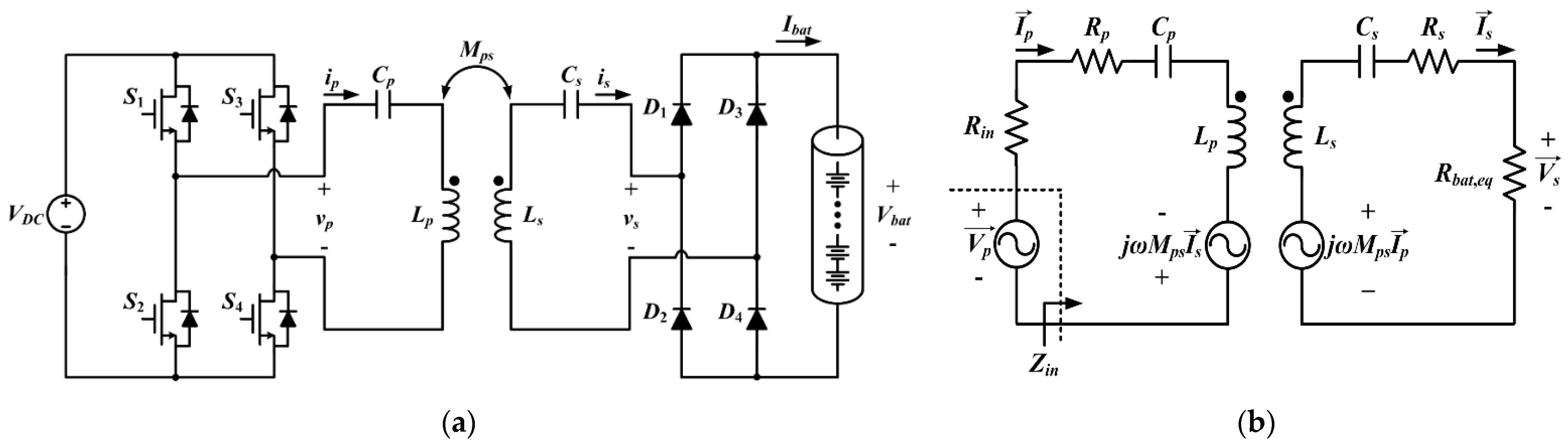
2. Single-Stage Wireless Battery Charging Circuit

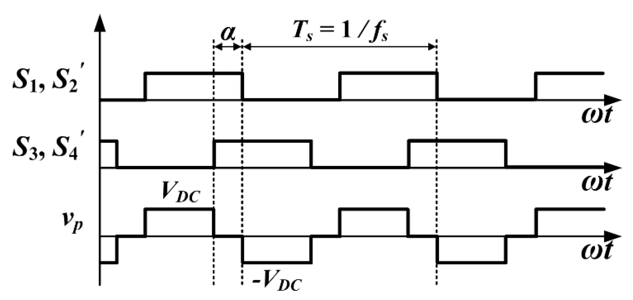
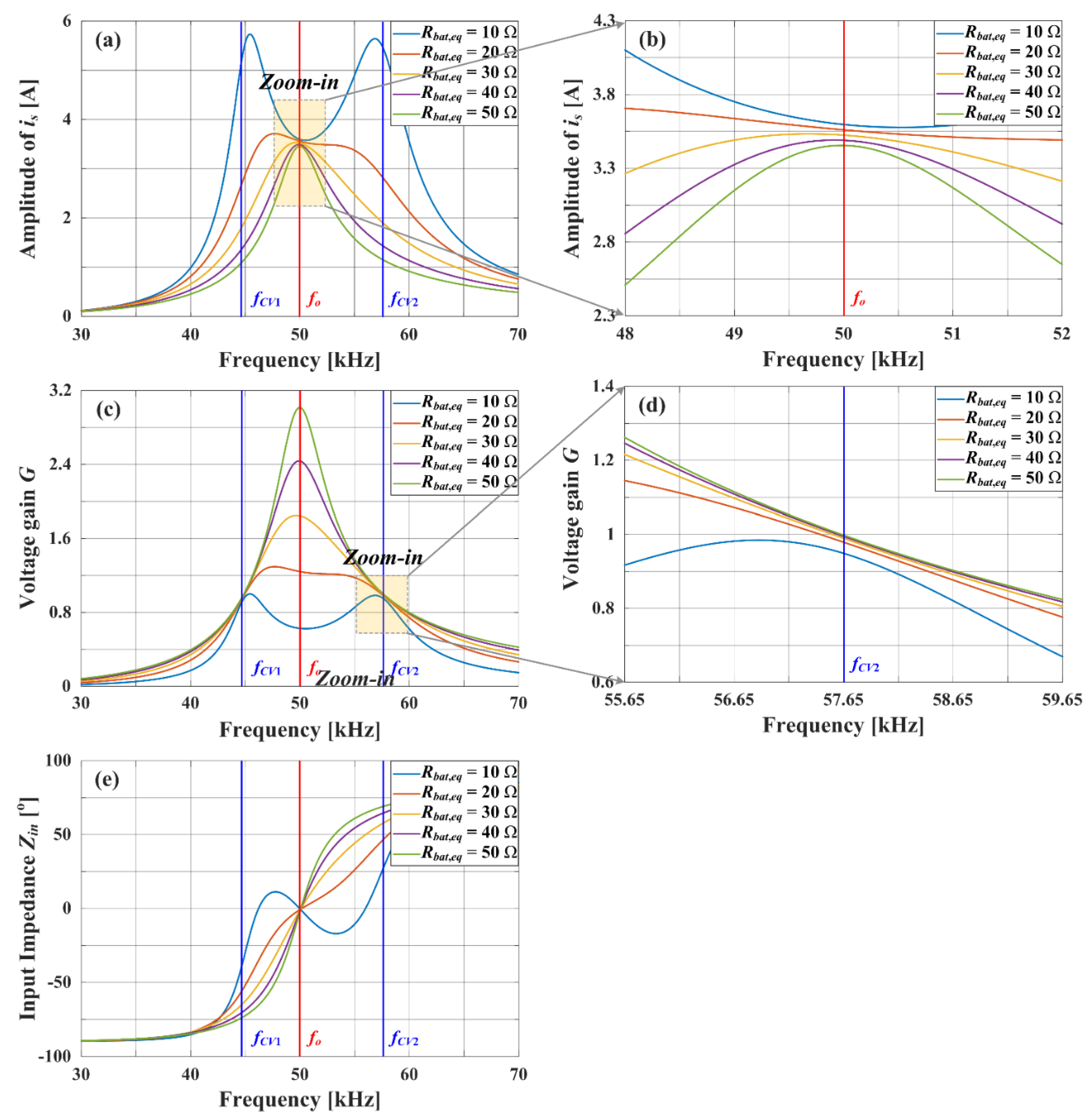
2.1. Circuit Structure and Analysis of Equivalent Circuit

The proposed single-stage wireless battery charging circuit (Figure 3a) consists of a full bridge inverter (S1S4) with transmitter coil (Lp) in the primary side and full bridge rectifier (D1D4) with receiver coil (Ls) in the secondary side. The two coils are serially compensated by the capacitors (Cp, Cs), and have a mutual inductance of M p s = k p s L p L s , where kps is the coupling coefficient between two coils. To maximize the output power capability, two coils are designed to have the same resonant frequency as ωo = 2π⸱fo; LpCp = LsCs = 1/ωo2. The two complementary switch pairs (S1, S2′ and S3, S4′) operate at the switching frequency fs = 1/Ts and are phase-shifted by an angle of α, so the output voltage of the full bridge inverter (vp) can be expressed as in Figure 4, where VDC is supplied DC voltage. Based on the FHA, the voltage and current of the proposed circuit in Figure 3 can be expressed as follows:
v p ( t ) = V p sin ( ω t + θ + φ ) = 2 V D C π ( 1 + cos α ) sin ( ω t + θ + φ ) ,
i p ( t ) = I p sin ( ω t + θ ) ,
v s ( t ) = V s sin ω t = 4 V b a t π sin ω t ,
i s ( t ) = I s sin ω t = π I b a t 2 sin ω t ,
where the subscripts p and s stand for the primary and secondary, Vbat is the voltage of the battery pack and Ibat is the charging current of the battery pack. Then, an equivalent of the proposed circuit is shown in Figure 3b, where Rin, Rp and Rs are equivalent series resistance (ESR) of full bridge inverter, primary coil and secondary coil, respectively. Rbat,eq is the equivalent load resistance of the battery pack, which can be expressed as:
R b a t , e q = V s I s = 8 π 2 R b a t .
If the Kirchhoff’s voltage law (KVL) is applied to the Figure 3b:
V p = ( R i n + Z p ) I p j ω M p s I s ,
j ω M p s I p = ( Z s + R b a t , e q ) I s ,
where Zp and Zs are impedance of the transmitter and receiver coil as Zp = Rp + jωLp + 1/jωCp and Zs = Rs + jωLs + 1/jωCs. From (6) and (7), amplitude of is, Is (Figure 5a), voltage conversion ratio G (Figure 5c), and input impedance Zin (Figure 5e) of the proposed circuit can be expressed as:
| I s | = | j ω M p s ( R i n + Z p ) ( Z s + R b a t , e q ) + ω 2 M p s 2 | | V p | .
G = | V s V p | = | R b a t , e q I s V p | = | j ω M p s R b a t , e q ( R i n + Z p ) ( Z s + R b a t , e q ) + ω 2 M p s 2 | ,
Z i n = V p I p = ( R i n + Z p ) ( Z s + R b a t , e q ) + ω 2 M p s 2 Z s + R b a t , e q ,

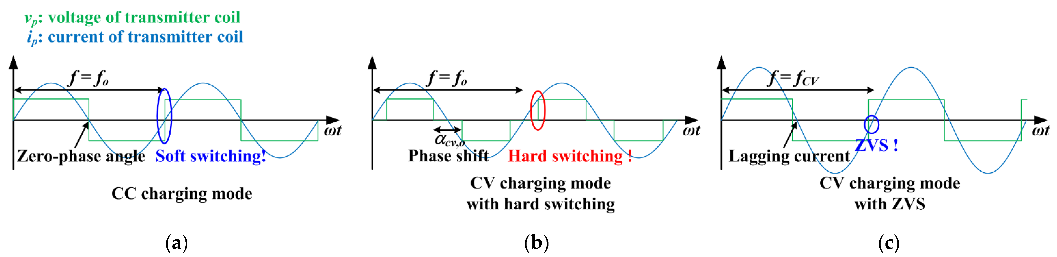
2.2. Anlaysis of Circuit for CC-CV Charging Mode

Normally, a battery charger has a CC-CV charging profile. At first, the battery pack is charged by the CC mode. When the Vbat reaches the cut-off voltage (Vbat,cut), the charging mode is changed to the CV mode, and the Ibat gradually decreases. Finally, the charging operation is terminated when the Ibat tapers to the end of the charging current (Iend) [8,9,10,12,13]. To support both modes, the proposed WPT circuit adopts the S-S-compensated network as in Figure 1.
At fs = fo, Zp = Rp and Zs = Rs, so (8) can be represented as:
I s = ω o M p s V p ( R i n + R p ) ( R s + R b a t , e q ) + ω o 2 M p s 2 | f s = f o .
If ESRs are negligible, Is = Vp/ωoMps, which means the circuit operates in CC regardless of Rbat,eq. However, ESRs inevitably exist in the circuit, and they affect the CC regulation as in Figure 5b. Thus, the operation of circuit at fs = fo with phase-shift of αCC guarantees the CC charging profile. From (1) and (11),
α C C = cos 1 { π 2 4 I c c [ ( R i n + R p ) ( R s + R b a t , e q ) + ω o 2 M p s 2 ] V D C ω o M p s 1 } ,
where Icc is the value of CC.
If the circuit still operates at fs = fo to get a CV, (9) can be arranged as
G = ω o M p s R b a t , e q ( R i n + R p ) ( R s + R b a t , e q ) + ω o 2 M p s 2 V p | f s = f o .
When ESRs are negligible, G = Rbat,eq/ωoMps, which means G depends on Rbat,eq, and the circuit cannot attain CV. Thus, the phase αcv,o to be compensated in the full bridge inverter is derived from (1) and (13) as
α c v , o = cos 1 { 2 V c v [ ( R i n + R p ) ( R s + R b a t , e q ) + ω o 2 M p s 2 ] V D C R b a t , e q ω o M p s 1 } ,
where Vcv is the value of CV. However, αcv,o is proportional to Rbat,eq, and it generates a hard switching condition because αcv,o is larger than ∠Zin at fs = fo (Figure 2b and Figure 6a).
To tackle this issue, the proposed circuit operates at a specific frequency fCV, where CV and ZVS are secured regardless of Rbat,eq. When the circuit operates in the CV mode, G should have a constant value regardless of Rbat,eq. If ESRs are negligible at (9), G can be expressed as
G | j ω M p s ( j ω L p + 1 / j ω C p ) + β / R b a t , e q | ,
where β = ω 2 C p C s ( M p s 2 L p L s ) + ( C p L p + C s L s ) 1 / ω 2 . If β is set to zero, the fCV, which guarantees the CV, is derived as ω C V 1 = 2 π f C V 1 = 2 π f o / 1 + k p s and ω C V 2 = 2 π f C V 2 = 2 π f o / 1 k p s . To achieve the ZVS operation of S1S4, ∠Zin at fs = fCV should be larger than zero as in Figure 5e, so fCV2 is desirable as fCV. Consequently, the operation of the circuit at fCV derives CV as G L s / L p . However, the inevitable ESRs affect the CV regulation as in Figure 5d, so the phase αCV to be compensated is derived from (1), (3) and (9) as
α C V = cos 1 { 2 V C V V D C ω C V M p s R b a t , e q [ ( R i n + R p ) ( R s + R b a t , e q ) ( ω C V c v L p 1 / ω C V C p ) ( ω C V L s 1 / ω C V C s ) + ω C V 2 M p s 2 ] 2 + [ ( R i n + R p ) ( ω C V L s 1 / ω C V C s ) + ( R s + R b a t , e q ) ( ω C V L p 1 / ω C V C p ) ] 2 1 } .
Because αCV is larger than ∠Zin at fs = fCV in whole range of Rbat,eq (Figure 6b), the ZVS operation is secured.
Finally, the proposed single-stage wireless battery charging circuit uses the proportional integral (PI) controller to track the αCC for ICC and αCV for VCV. The only issue is finding kps to operate the circuit at f C V = f o / 1 k p s in the CV mode. In the following section, the method to find kps and the composition of the controller will be presented.

2.3. Coupling Coefficient Prediction Method and Control of CC-CV Charging Mode

The output current and voltage regulation characteristics are affected by the ESRs, load resistance and operating frequency as expressed in the above section. Also, because kps is changed by variable coil alignment, the CV mode at fs = fCV has been unpractical. Therefore, additional circuits, complex control algorithms or pre-measured kps have been used to charge the battery pack [8,9,10,11,12,13,14,15,16]. We introduce the prediction method of kps, which can be used to calculate fCV. Also, we incorporate this method to the phase-shift technique to charge a battery pack in CC-CV mode.
When the proposed WPT system operates in CC modes at fo, Ibat can be expressed as follows by using (1), (4), (5), (11):
I b a t = 4 π 2 ω o M p s V D C ( cos α C C + 1 ) ( R i n + R p ) ( R s + 8 V b a t / π 2 I b a t ) + ω o 2 M p s 2 .
It can be rearranged according to Mps as:
( π 4 ω o 2 I b a t 2 ) M p s 2 4 π 2 V D C ω o I b a t ( cos α C C + 1 ) M p s + π 2 I b a t ( R i n + R p ) ( π 2 R s I b a t + 8 V b a t ) = 0
This equation has two solutions for Mps, and the larger one is a reasonable value according to the calculation result, so
M p s = b + b 2 a c a ,
where a = π 4 ω o 2 I b a t 2 , b = 2 π 2 V D C ω o I b a t ( cos α C C + 1 ) , c = π 2 I b a t ( R i n + R p ) ( π 2 R s I b a t + 8 V b a t ) .
Because the value of αCC, ωo, Rin, Rp and Rs is known, and the DC value of VDC, Vbat and Ibat is easily sensed, kps can be predicted by k p s , p d = M p s , p d / L p L s , where the subscript pd stands for prediction.
Finally, the controller for the proposed single-stage wireless battery charging circuit can be designed as in Figure 7, and it consists of an operating algorithm with kps prediction, PI control part for the αCC and αCV, CC and CV mode selector part, gate signal conditioning part and protection part for over-charging the voltage/current (Voc, Ioc). The main controller is implemented by TMS320F28335, which has a 12-bit analog-to-digital converter. The gate signal block is modulated by an enhanced pulse width modulator (ePWM) module, and other parts including an algorithm, PI controller, mode selector and protection are operated by the interrupt function of ADC block. The operating algorithm consists of the following eight procedures:
(1)
If Vbat[n] < Vbat,cut, the circuit operates in the CC mode, otherwise the circuit terminates the charging operation.
(2)
To regulate the Ibat as ICC, fs is set to fo, and the PI controller compensates the phase αCC[n].
(3)
By using (18), kps,pd[n] is continuously updated to check the variation of coil alignment.
(4)
The algorithm repeats (2) and (3) until Vbat[n] = Vbat,cut.
(5)
At the instant of Vbat[n] = Vbat,cut, fCV is calculated based on the final updated kps,pd[n].
(6)
The CC mode is changed to the CV mode. The transition mode consists of two sequences; (a) The transferred power is decreased to zero by gradually increasing αCC[n] to π. (b) fs is set to fCV, and the circuit renews the CV mode.
(7)
To regulate the Vbat as VCV, the PI controller compensates the phase αCV[n].
(8)
If Ibat has tapper to Iend, the total charging operation for the battery pack is finished, otherwise it continuously operates the CV mode as in (7).

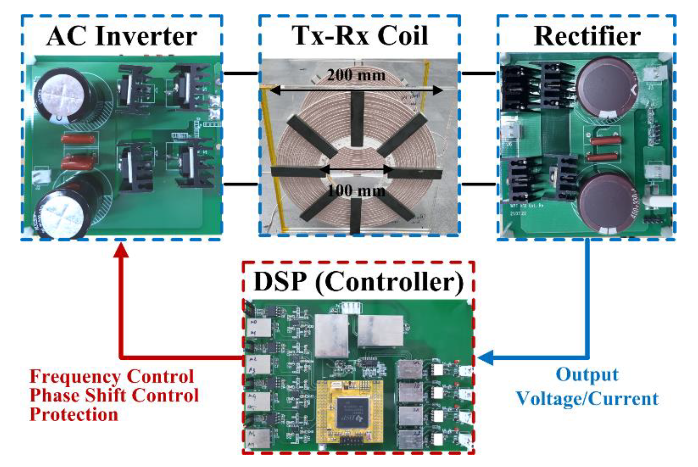
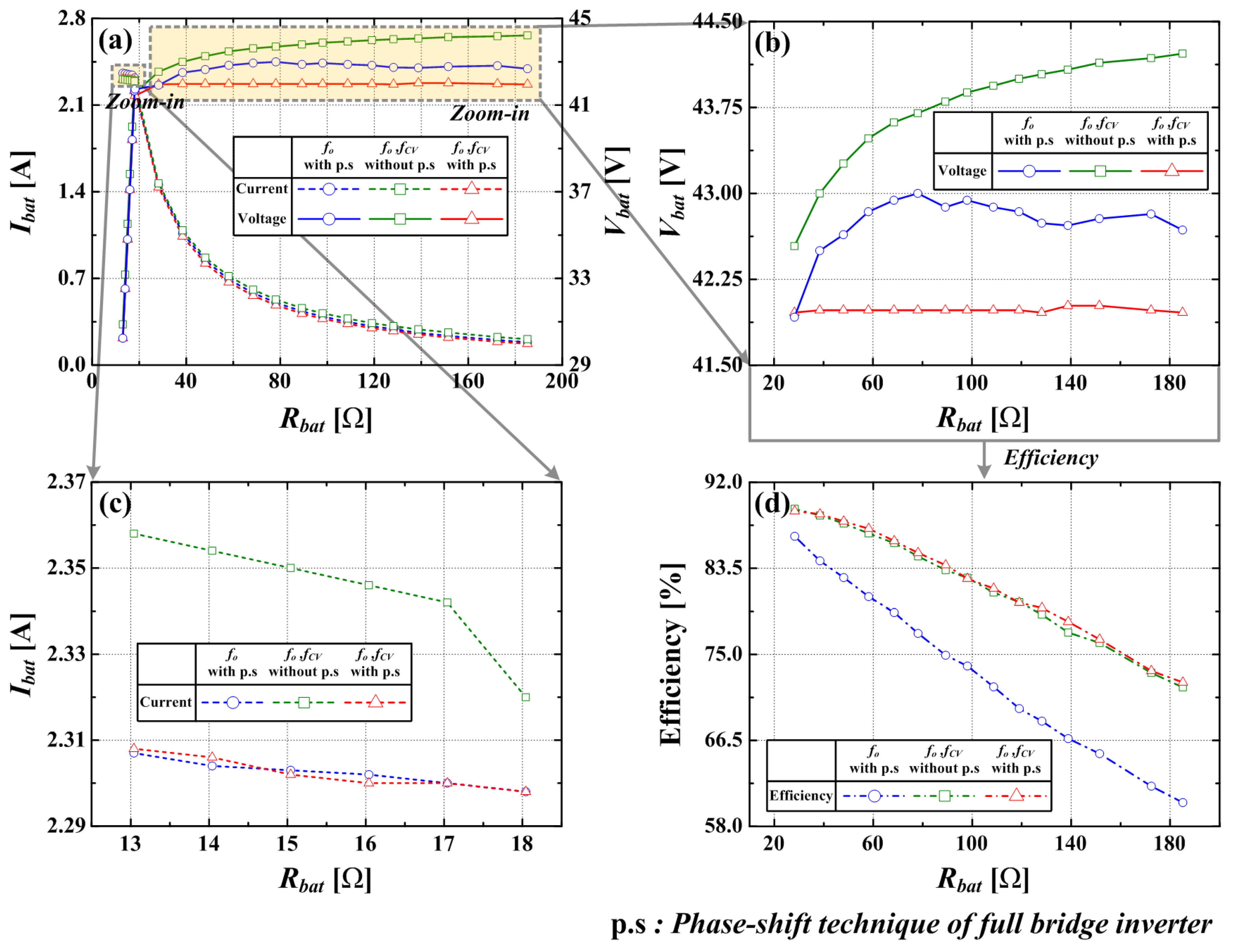
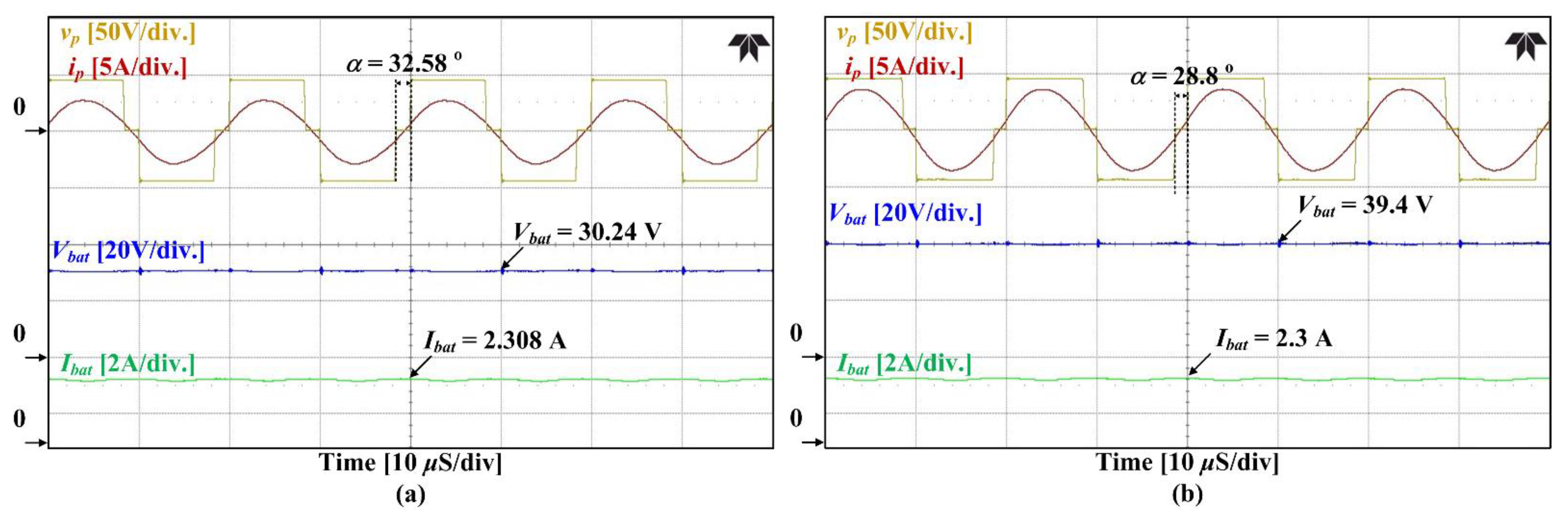
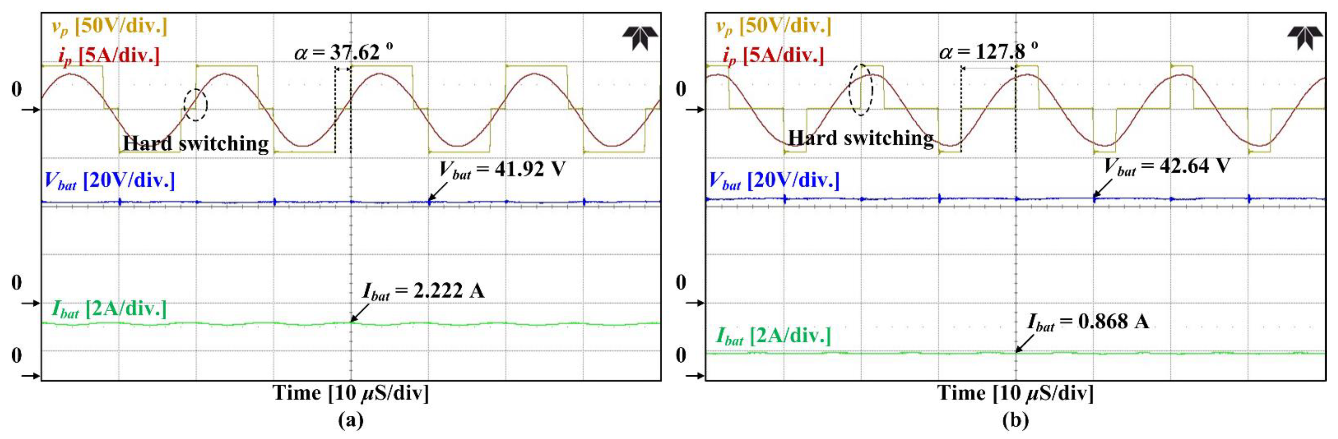
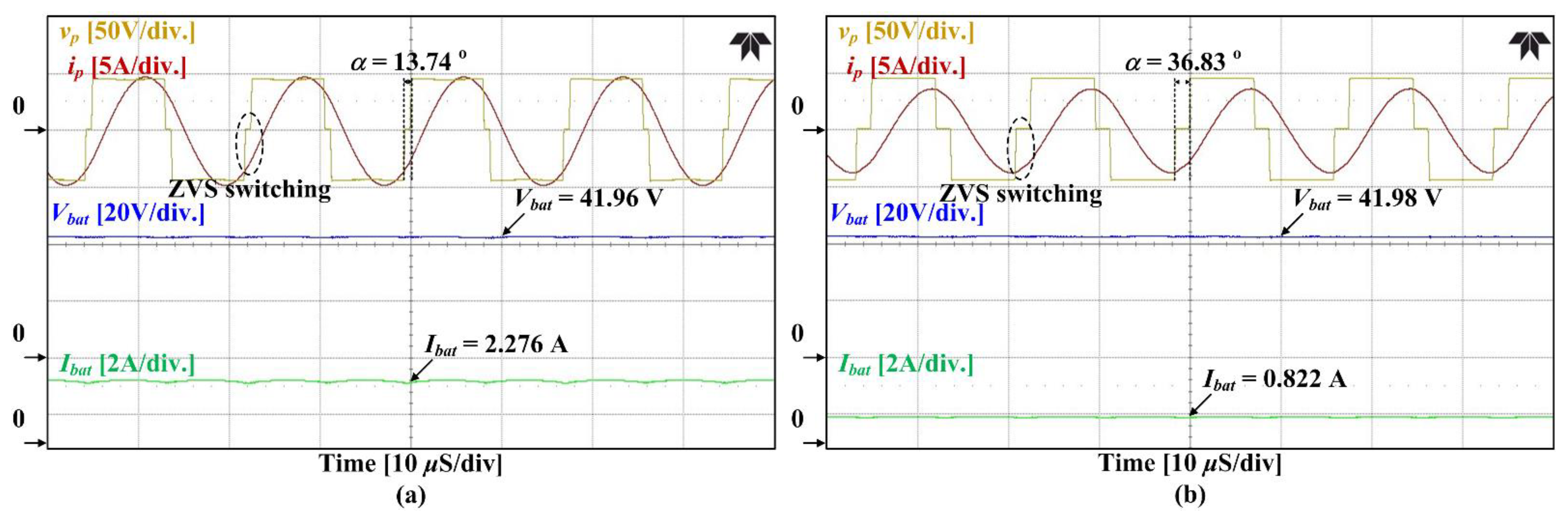
3. Experimental Results

The prototype (Figure 8) was built and tested to prove the proposed single-stage wireless battery charging circuit. The battery pack was emulated by an electrical load (PLZ1004WH; Kikusui, Co., Ltd.), and the voltage range of the emulated battery pack was set to 30~42 V; 10 serially connected Li-ion battery cells. The simulated battery pack of the equivalent (Rbat) was 13.04~18.26 Ω in the CC mode having ICC = 2.3 A and 18.26~182.6 Ω in the CV mode having VCV = 42 V and Iend = 0.23 A. The inner diameter of the transmitter and receiver coil was 100 mm, the outer diameter was 200 mm, and the fo was set to 50 kHz.
The turns ratio of two coils was 1:1, so VDC = 45 V from V s V p L s / L p . The values of circuit parameters and circuit components are given in Table 1.
At first, the values of measured kps and Mps were compared with the kps,pd and Mps,pd in the alignment and misalignment conditions as in Table 2. The location of two coils were set by using an orthogonal coordinate; the transmitter coil was located at x = 0 cm, y = 0 cm, and receiver coil was located at x = 6 cm, y = 0 cm in the alignment condition and x = 6 cm, y = 2cm in the misalignment condition. The kps and Mps in the alignment condition were 0.2479 and 50.1795 μH, respectively. The prediction was implemented in the whole voltage range of Vbat, and kps,pd was in the range of 0.2463~0.2469; 0.41~0.62% errors. Mps,pd was calculated based on M p s , p d = k p s , p d L p L s , and in the range of 49.8663~49.9645 μH; 0.43~0.52% errors. When the coils were located in the misalignment condition, the kps and Mps were 0.2402 and 48.6187 μH, respectively. The kps,pd was in the range of 0.2357~0.2363, and Mps,pd was in the range of 47.7272~47.7593 μH; 1.63~1.85%, and 1.77~1.83% errors, respectively.
The regulation capability of the single-stage wireless battery charging circuit was tested at x = 6 cm, y = 0 cm as Figure 9a–c. When the circuit operates in fs = fo in the CC mode, Ibat was in the range of 2.32~2.358 A at 13.04 Ω < Rbat < 18.26 Ω. The variation of Ibat was 38 mA due to the effect of parasitic components as in (11). To complement this effect, the phase-shift technique was applied to the full bridge inverter. The compensated phase α was 32.58° at Rbat = 13.04 Ω and 28.8° at Rbat = 17.04 Ω as Figure 10. The regulated Ibat in the CC mode was in the range of 2.298~2.308 A (Figure 9c), and the variation of Ibat was improved from 38 mA to 10 mA owing to the phase-shift technique. When Vbat reached 42 V at Rbat = 18.26 Ω, the operational mode of the circuit was changed to CV mode. Because the circuit still operated at fs = fo, it is difficult to attain the CV characteristic regardless of Rbat as in Figure 5c. Thus, the circuit compensated α for maintaining Vbat was 37.62° at Rbat = 18.29 Ω and increased to 127.8° at Rbat = 41.53 Ω as in Figure 11. Consequently, Vbat was regulated in the range of 41.92~43 V, and variation of Vbat was 1.08 V as Figure 9b. However, the full bridge inverter operated in the hard switching condition across the whole range of Rbat as in Figure 10, and the power efficiency was measured at 86.65–60.35% in CV mode as in Figure 9d.
To improve the performance of the single-stage wireless battery charging circuit, the circuit can operate in fs = fCV, where the circuit has the CV characteristic and ZVS operating condition. Because kps,pd was 0.2469 at x = 6 cm and y = 0 cm, the fCV was set to 57.616 kHz by using f C V = f o / 1 k p s . As a result, the power efficiency was measured at 89.37–71.74% in CV mode as in Figure 9d, which was 2.72–11.39% higher than the operation at fs = fo with phase-shift technique. Even though the power efficiency increased owing to the ZVS operation, Vbat was regulated in the range of 42.54–44.22 V (Figure 9b). The variation of Vbat was 1.68 V, which was 0.6 V higher than the operation at fs = fo with phase-shift technique. This means that the parasitic components still influence the voltage regulation. To solve this issue, the phase-shift technique of the full bridge inverter was introduced to the circuit, the compensated α for maintaining Vbat was measured as 13.74° at Rbat = 18.29 Ω and increased to 36.83° at Rbat = 41.53 Ω as in Figure 12. Consequently, Vbat was regulated in the range of 41.96–42.02 V, and the variation of Vbat was only 6 mV as Figure 9b. In addition to the improved Vbat regulation, the waveforms in Figure 12 show that the circuit achieved ZVS operation condition across the whole range of Rbat. Therefore, the power efficiency was measured at 89.14–72.23% as in Figure 9d, which was 2.49–11.88% higher than the operation at fs = fo with the phase-shift technique.

4. Conclusions

In this paper, a single-stage wireless battery charging circuit is proposed. This circuit implements the CC charging mode at the resonant frequency of two coils and the CV charging mode based on the proposed coupling coefficient prediction method; the predicted value is used to calculate the operating frequency of the circuit, which stands for CV output characteristic and ZVS operating condition of the circuit. Additionally, the proposed circuit adopts the phase-shift technique at the full bridge inverter to improve the output current/voltage regulation capability in the CC/CV modes. The prototype was tested for its ability to charge a 36 V battery pack, and the resonant frequency of the transmitter/receiver coils was set to 50 kHz. The experimental circuit predicted a coupling coefficient within 0.62% error in the coil alignment condition. By incorporating this predicted value to the circuit with phase-shift technique, the experimental circuit successfully improved power efficiency using the ZVS operation in the CV mode, and achieved CC and CV regulation within 0.32% error in the CC mode and 0.1% error in the CV mode, respectively.

Author Contributions

Conceptualization, S.-W.L. and Y.-K.C.; methodology, S.-W.L. and Y.-K.C.; software, S.-W.L.; validation, S.-W.L. and Y.-K.C.; formal analysis, S.-W.L. and Y.-K.C.; investigation, Y.-K.C.; resources, Y.-K.C.; data curation, S.-W.L. and Y.-K.C.; writing—original draft preparation, S.-W.L.; writing—review and editing, Y.-K.C.; visualization, S.-W.L.; supervision, Y.-K.C.; project administration, S.-W.L. and Y.-K.C.; funding acquisition, S.-W.L. All authors have read and agreed to the published version of the manuscript.

Funding

This research was supported by Basic Science Research Program through the National Research Foundation of Korea (NRF) funded by the Ministry of Education (2021R1I1A3050095). This work was supported by the research grant of the Kongju National University in 2021.

Conflicts of Interest

The authors declare no conflict of interest.

References

  1. Andrea, B.; Michele, B.; Alfio, D.G. A review of power management integrated circuits for ultra sound-based energy harvesting in implantable medical devices. Appl. Sci. 2021, 11, 2487. [Google Scholar]
  2. Andrea, B.; Alfio, D.; Gaetano., P. Charge pump improvement for energy harvesting applications by node pre-charging. IEEE Trans. 2020, 67, 3312–3316. [Google Scholar]
  3. Shin, J.; Shin, S.; Kim, Y.; Ahn, S.; Lee, S.; Jung, G.; Jeon, S.J.; Cho, D.H. Design and implementation of shaped magnetic-resonance-based wireless power transfer system for roadway-powered moving electric vehicles. IEEE Trans. Ind. Electron. 2015, 61, 1179–1192. [Google Scholar] [CrossRef]
  4. Kim, J.W.; Son, H.C.; Kim, D.H.; Park, Y.J. Optimal design of a wireless power transfer system with multiple self-resonators for an led tv. IEEE Trans. Consum. Electron. 2012, 58, 775–780. [Google Scholar] [CrossRef]
  5. Stielau, O.H.; Covic, G.A. Design of loosely coupled inductive power transfer systems. In Proceedings of the International Conference of Power System Technology, Perth, Australia, 4–7 December 2000; pp. 85–90. [Google Scholar]
  6. Wang, C.S.; Stielau, O.H.; Covic, G.A. Design considerations for a contactless electric vehicle battery charger. IEEE Trans. Ind. Electron. 2005, 52, 1308–1314. [Google Scholar] [CrossRef]
  7. Bosshard, R.; Kolar, J.W.; Mühlethaler, J.; Stevanović, I.; Wunsch, B.; Canales, F. Modeling and η-α-pareto optimization of inductive power transfer coils for electric vehicles. IEEE J. Emerg. Sel. Top. Power Electron. 2015, 3, 50–64. [Google Scholar] [CrossRef]
  8. Babaki, A.; Zadeh, S.V.; Zakerian, A. Performance optimization of dynamic wireless ev charger under varying driving conditions without resonant information. IEEE Trans. Veh. Tech. 2019, 68, 10429–10438. [Google Scholar] [CrossRef]
  9. Lee, Y.D.; Kim, D.M.; Kim, C.E.; Moon, G.W. A new receiver-side integrated regulator with phase shift control strategy for wireless power transfer system. In Proceedings of the IEEE PELS Workshop on Emerging Technologies, Seoul, Korea, 15–19 November 2020; pp. 112–115. [Google Scholar]
  10. Li, S.; Mi, C.C. Wireless power transfer for electric vehicle application. IEEE J. Emerg. Sel. Top. Power Electron. 2015, 3, 4–17. [Google Scholar]
  11. Covic, G.A.; Boys, J.T. Modern trends in inductive power transfer for transportation application. IEEE J. Emerg. Sel. Top. Power Electron. 2013, 1, 28–41. [Google Scholar] [CrossRef]
  12. Zheng, C.; Lai, J.S.; Chen, R.; Faraci, W.E.; Zahid, Z.U.; Gu, B.; Zhang, L.; Lisi, G.; Anderson, D. High efficiency contactless power transfer system for electric vehicle battery charging application. IEEE J. Emerg. Sel. Top. Power Electron. 2015, 3, 65–74. [Google Scholar] [CrossRef]
  13. Tran, D.H.; Vu, V.B.; Choi, W. Design of a high-efficiency wireless power transfer system with intermediate coils for the on-board chargers of electric vehicles. IEEE Trans. Power Electron. 2018, 33, 175–187. [Google Scholar] [CrossRef]
  14. Qu, X.; Han, H.; Wong, S.C.; Tse, C.K.; Chen, W. Hybrid IPT topologies with constant current or constant voltage output for battery charging applications. IEEE Trans. Power Electron. 2015, 30, 6329–6337. [Google Scholar] [CrossRef]
  15. Mai, R.; Chen, Y.; Li, Y.; Zhang, Y.; Cao, G.; He, Z. Inductive power transfer for massive electric bicycles charging based on hybrid topology switching with a single inverter. IEEE Trans. Power Electron. 2017, 32, 5897–5906. [Google Scholar] [CrossRef]
  16. Chen, Y.; Mai, R.; Zhang, Y.; He, Z. Inductive power transfer for electric bicycles charging based on variable compensation capacitor. In Proceedings of the IEEE Conference on Applied Power Electronics Conference and Exposition, Tampa, FL, USA, 26–30 March 2017; pp. 1389–1393. [Google Scholar]
Figure 1. (a) Multi-stage wireless battery charging circuit; (b) single-stage wireless battery charging circuit.
Electronics 10 02615 g001
Figure 2. Ideal voltage and current of transmitter coil in (a) constant current charging mode without phase shift control at f = fo; (b) constant voltage charging mode at f = fo with phase shift control; (c) constant voltage charging mode without phase shift control at f = fCV.
Electronics 10 02615 g002
Figure 3. (a) Schematic diagram of the proposed single-stage wireless battery charging circuit; (b) Equivalent of the proposed circuit.
Electronics 10 02615 g003
Figure 4. The gate signals and output voltage waveform of the full bridge inverter.
Electronics 10 02615 g004
Figure 5. Electrical characteristics of single-stage wireless battery charging circuit, when VDC = 45 V, α = 0, Lp = 201.89 μH, Ls = 202.9 μH, Cp = 50.05 nF, Cs = 49.92 nF, Mps = 50. 17 μH, Rin = 12 mΩ, Rp = 242 mΩ and Rs = 392 mΩ. (a) amplitude of is; (b) zoom-in waveform of Is; (c) voltage gain G; (d) zoom-in waveform of G; (e) Phase of input impedance Zin.
Electronics 10 02615 g005
Figure 6. Comparison of phase between (a) ∠Zin and αcv,o at fs = fo, (b) ∠Zin and αCV at fs = fCV.
Electronics 10 02615 g006
Figure 7. Block diagram of the digital controller for the proposed single-stage wireless battery charging circuit.
Electronics 10 02615 g007
Figure 8. Prototype of the proposed single-stage wireless battery charging circuit.
Electronics 10 02615 g008
Figure 9. Comparison of Vbat, Ibat regulation and power efficiency by using kps,pd and Mps,pd. The receiver coil was located at x = 6 cm, y = 0 cm. (a) Ibat and Vbat regulation result, (b) zoom-in waveform of voltage regulation, (c) zoom-in waveform of current regulation, and (d) power efficiency in CV mode.
Electronics 10 02615 g009
Figure 10. Experimental waveforms when the proposed WPT circuit operates in the CC mode with fs = fo at (a) Rbat = 13.04 Ω, and (b) Rbat = 17.04 Ω.
Electronics 10 02615 g010
Figure 11. Experimental waveforms when the proposed WPT circuit operates in the CV mode with fs = fo at (a) Rbat = 18.29 Ω, and (b) Rbat = 41.53 Ω.
Electronics 10 02615 g011
Figure 12. Experimental waveforms when the proposed WPT circuit operates in the CV mode with fs = fCV at (a) Rbat = 18.29 Ω, and (b) Rbat = 41.53 Ω.
Electronics 10 02615 g012
Table 1. Parameter values and components of the experimental circuit.
SymbolValue/Model
Lp, Ls201.89 μH, 202.9 μH
Cp, Cs50.05 nF, 49.92 nF
Rin, Rp, Rs13 mΩ, 242 mΩ, 210 mΩ
S1S4FDP075N15A
D1D430ETH06
ControllerTMS320F28335
Table 2. Prediction results of kps and Mps in the range of Vbat = 30~42 V.
AlignmentVbat [V]kpskps,pd
(Error %)
Mps [μH]Mps,pd [μH]
(Error %)
x = 6 cm, y = 0 cm300.24790.2465 (0.5508)50.179549.8663 (0.6242)
320.2463 (0.6211)49.9073 (0.5424)
340.2464 (0.6077)49.9136 (0.5299)
360.2467 (0.4744)49.9645 (0.4284)
380.2467 (0.4880)49.9011 (0.5547)
400.2468 (0.4256)49.9305 (0.4963)
420.2469 (0.4070)49.9610 (0.4355)
x = 6 cm, y = 2 cm300.24020.2363 (1.6304)48.618747.7593 (1.7676)
320.2359 (1.7761)47.7291 (1.8298)
340.2359 (1.7835)47.7416 (1.8041)
360.2360 (1.7497)47.7314 (1.8250)
380.2357 (1.8512)47.7294 (1.8291)
400.2359 (1.7823)47.7272 (1.8336)
420.2359 (1.7939)47.7483 (1.7903)
Publisher’s Note: MDPI stays neutral with regard to jurisdictional claims in published maps and institutional affiliations.

