Article

A Simple Virtual-Vector-Based PWM Formulation for Multilevel Three-Phase Neutral-Point-Clamped DC–AC Converters including the Overmodulation Region

by
Sergio Busquets-Monge
Department of Electronic Engineering, Universitat Politècnica de Catalunya, 08034 Barcelona, Spain
Electronics 2022, 11(4), 641; https://doi.org/10.3390/electronics11040641
Submission received: 31 December 2021 / Revised: 10 February 2022 / Accepted: 14 February 2022 / Published: 18 February 2022
(This article belongs to the Special Issue Power Electronics and Control of High-Speed Electrical Drives)

Abstract

:
Neutral-point-clamped (NPC) power conversion topologies are among the most popular multilevel topologies in current industrial products and in industrial and academic research. The proper operation of multilevel three-phase NPC DC–AC converters requires the use of specific pulse-width modulation (PWM) strategies that maintain the DC-link capacitor voltage balance and concurrently optimize various performance factors such as efficiency and harmonic distortion. Although several such PWM strategies have been proposed in the literature, their formulation is often complex and/or covers only particular cases and operating conditions. This manuscript presents a simple formulation of the original virtual-vector-based PWM, which enables capacitor voltage balance in every switching cycle. The formulation is presented, for the general case, in terms of basic phase voltage modulating signals, with no reference to space vectors, involving any number of levels and for any operating conditions, including the overmodulation region. The equivalence of the presented formulation to the original PWM strategy is demonstrated through simulation under different scenarios and operating conditions. Thus, this manuscript offers in a one-stop source a simple, effective, and comprehensive PWM formulation to operate multilevel three-phase NPC DC–AC converters with any number of levels in any operating condition.

1. Introduction

One of the major application areas of power electronics is electrical motor drives [1,2] due to the substantial amount of systems that use an electric motor, the performance benefits achieved by driving the motor through a power converter, and the vast amount of energy that is processed by these systems.
Three-phase synchronous and asynchronous motors are the most popular, while they are often driven by a conventional two-level three-phase DC–AC voltage source converter, made of three two-level converter legs, as depicted in Figure 1a. However, the motor voltage, current, and corresponding power ratings vary substantially from one application to another, and this requires the use of different suitable power devices to configure the inverter for each case. An alternative solution is to use a multilevel topology to configure the motor drive, such as in the simple three-level example of Figure 1b. In this case, from a given robust power device with optimized performance and low cost, a range of motor drives at different voltage and power ratings can be configured by simply adjusting the number of levels. In addition, the multilevel converter brings additional benefits in terms of efficiency, harmonic distortion, electromagnetic compatibility, etc.
Different multilevel topologies can be considered for the purpose of assembling a motor drive [3,4,5,6,7]. These topologies can be broadly classified in the cascaded H-bridge, flying capacitors, and neutral-point-clamped (NPC) families. Among them, the NPC family is of special interest because it offers the greatest potential to maximize power density [8,9,10,11,12,13,14,15], since the converter legs, functionally equivalent to a single-pole multiple-throw switch, are configured only with a combination of semiconductor devices, without any capacitors, inductors, or transformers, which are otherwise needed in other converter families. Then, a single set of series-connected capacitors forms the common DC-link for all legs. However, the operation of NPC multilevel converters is challenging, as the balancing of the DC-link capacitor voltages is not straightforward. This problem has been widely reported and studied in the literature [16], where it has been demonstrated that traditional multilevel pulse-width modulation (PWM) strategies lack the capacity to balance the DC-link capacitor voltages, and the problem is especially serious at four and more levels for a wide range of operating conditions, since some of the capacitor voltages collapse. Fortunately, several special PWM strategies enable the multilevel NPC DC–AC converter operation for the full modulation range with capacitor voltage balance. These include virtual-vector-based PWMs (VVPWMs) [17,18,19,20,21,22,23,24,25,26,27,28,29,30,31,32], the carrier-overlapped PWM (COPWM) [33], and other variants [34].
As long as the sum of all phase currents equals zero and the phase current ripple is relatively small, VVPWMs guarantee the balance in every switching cycle, with the drawback of increasing the number of switching transitions and harmonic distortion as compared to conventional PWM strategies. They are applicable for any number of levels and phases, and they have been extended to the overmodulation region in the three-phase case. Being able to operate in the overmodulation region is important in motor drives to maximize the achievable motor speed for a given DC-link voltage. On the other hand, modulations such as the COPWM also reach capacitor voltage balance in all operating conditions featuring lower switching losses and harmonic distortion as compared to VVPWMs. Nevertheless, the balance is achieved in a line cycle, which calls for a much larger DC-link capacitance, especially in motor drives that should operate at low speeds. Additionally, they have only been defined for a limited number of levels (four levels) and the undermodulation or linear modulation range.
Therefore, this article will focus on multilevel NPC motor drives operated with VVPWMs, which represents a competitive solution already in use in industry, mainly at three levels. These PWM strategies were originally conceived and defined with the aid of the converter space vector diagram (SVD) [17,18]. Since their direct implementation from the SVD becomes quite complex, several efforts have been devoted to finding a simplified implementation through closed-form expressions defining the duty ratio of connection of each leg to each DC-link point or through the definition of an equivalent carrier-based PWM. This seems to be of major importance to facilitate a wide acceptance of these topologies. A simple PWM strategy implementation mitigates the difficulties associated with their inherent higher complexity, given that they introduce a higher number of switching devices.
In this context, this paper presents a novel and simplified formulation to implement VVPWMs for three-phase NPC DC–AC converters with any number of levels, including the operation in the overmodulation region.
The paper is organized as follows: In Section 2, a review of the basic NPC topologies and their operating principle is presented. In Section 3, the novel simplified VVPWM formulation is presented. In Section 4, the good performance and equivalence of this novel formulation to the original VVPWM strategy definition is proved through simulation. Finally, Section 5 presents the conclusions.

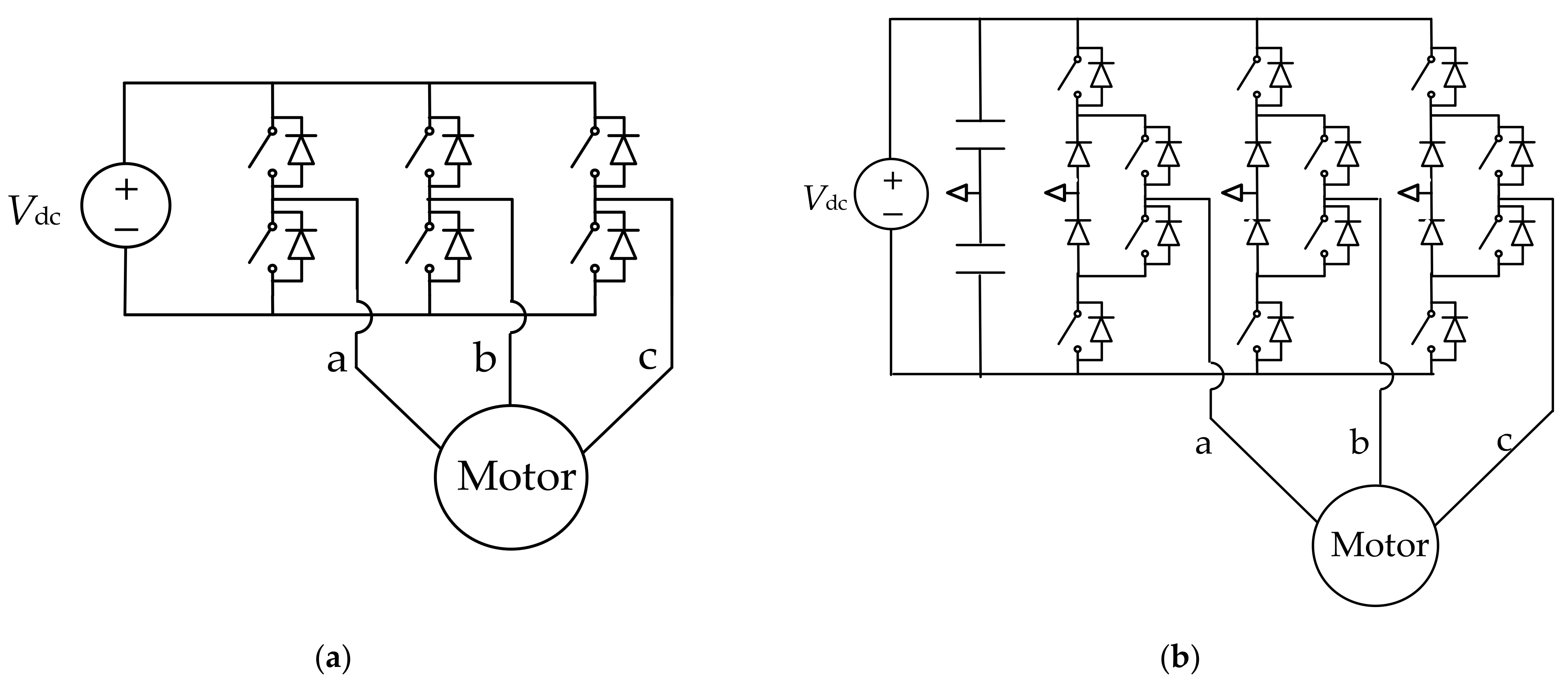
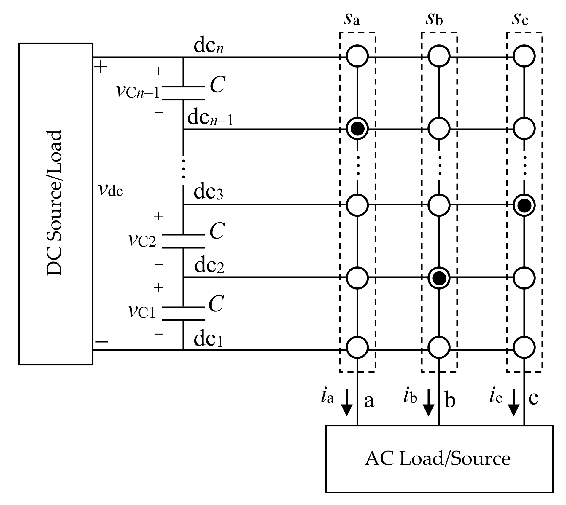
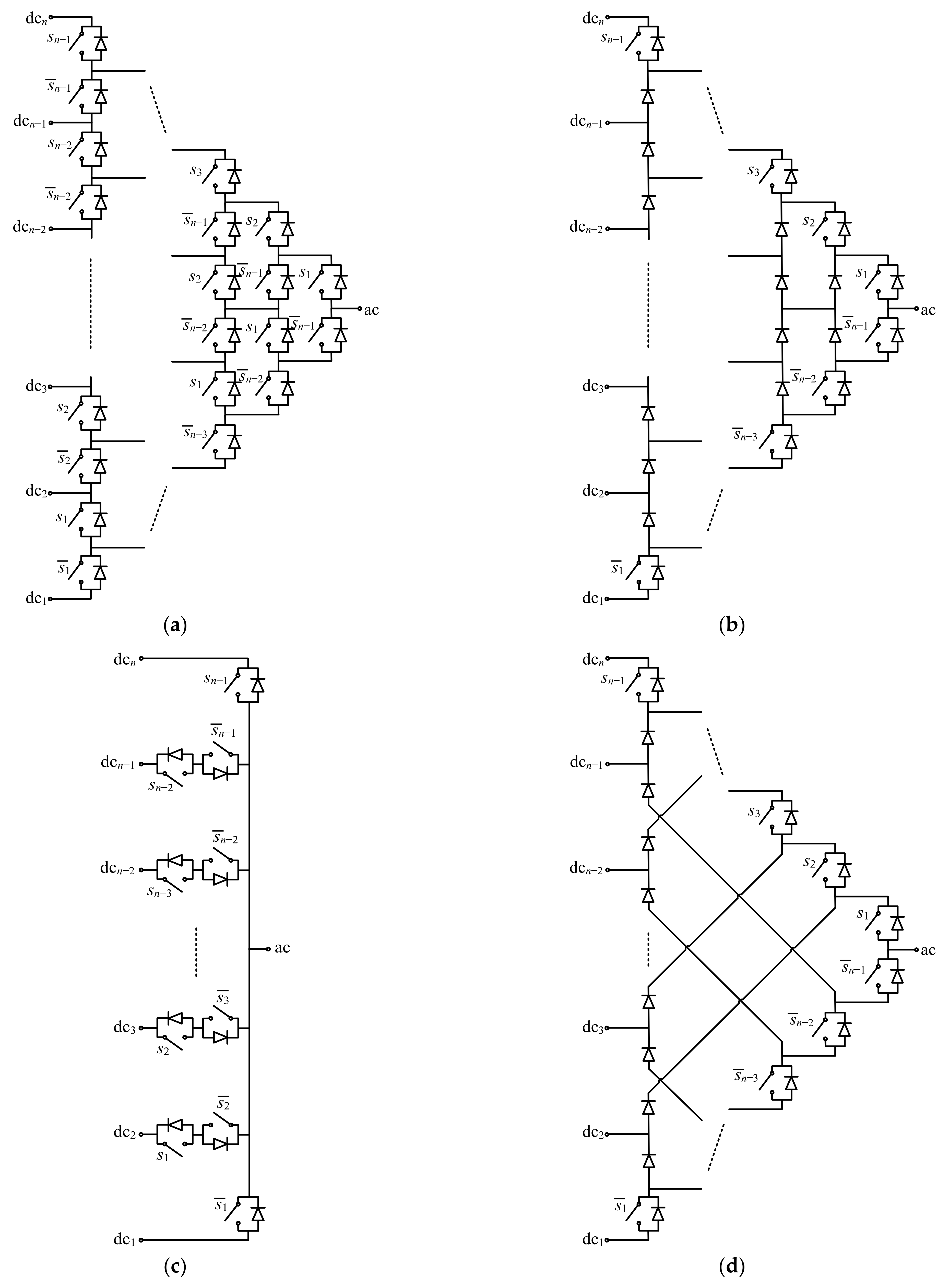
2. Review of NPC Topologies and Their Operating Principle

Pure multilevel NPC converters are built with a combination of converter legs, each functionally equivalent to a single-pole multiple-throw switch, as depicted in Figure 2. At every point in time, the leg AC terminal can be electrically connected to one of the DC-link points: to any of the two outer DC-link points dc1 and dcn, or to any of the n − 2 inner neutral points dc2 to dcn−1.
Several circuit topologies are possible to build such converter legs. The main topologies are shown in Figure 3 [9]. All of them combine a number of transistors and diodes to perform the single-pole multiple-throw switch function. Figure 3a presents the active or transistor-clamped NPC (ANPC) version of the topology built with a pyramidal connection of a single type of transistor with antiparallel diode, with a voltage rating equal to one elementary voltage level Vdc/(n − 1). Removing the inner transistors from the pyramid leads to the passive or diode-clamped NPC (PNPC) version of the topology, as shown in Figure 3b. The topologies in Figure 3a,b require a substantial number of devices, especially as the number of levels increases. In order to reduce the number of devices, some of the devices in Figure 3a,b can be combined into other devices with higher voltage rating, leading to the reduced ANPC and PNPC topologies shown in Figure 3c,d. Other topologies can be found in the literature designated as NPC but are in fact hybrid topologies combining the former topologies with others such as the flying capacitors. In this paper, these hybrid topologies are not considered, although the presented modulation strategy can be also adapted to many of them.
Figure 3 also indicates the binary control signal applied to every transistor (sk). A value equal to 1 indicates that the corresponding switch is on, while a 0 value indicates that the switch is off. It can be seen that the devices from the same diagonal share the same control signal, and that devices from negative diagonals feature the complementary signal of devices from positive diagonals. Overall, the leg presents n − 1 independent control signals, from s1 to sn−1. Table 1 defines the fundamental set of leg switching states to connect the leg AC terminal to each of the DC-link terminals [9]. It can be observed that the independent binary control signals follow a thermometric code.

3. Simplified Virtual-Vector-Based PWM Formulation

In this section, a novel and simple formulation of the original VVPWM [17,18] for multilevel three-phase NPC DC–AC converters, as shown in Figure 4, is presented, with the aim to facilitate its comprehension and implementation and provide additional insight. In Section 3.1, the formulation is initially presented for the undermodulation or linear modulation range. This range is characterized by a value of the modulation index m ∈ [0, 1], where m is defined as the ratio of the peak value of the fundamental phase-to-load-neutral voltage to its maximum value in the linear modulation range (m = vx,1,pk/(vdc/sqrt(3)), where x ∈ {a, b, c}). The formulation is later extended in Section 3.2 to the overmodulation range, covering the full range of m ∈ [0, 2·sqrt(3)/π = 1.1027].

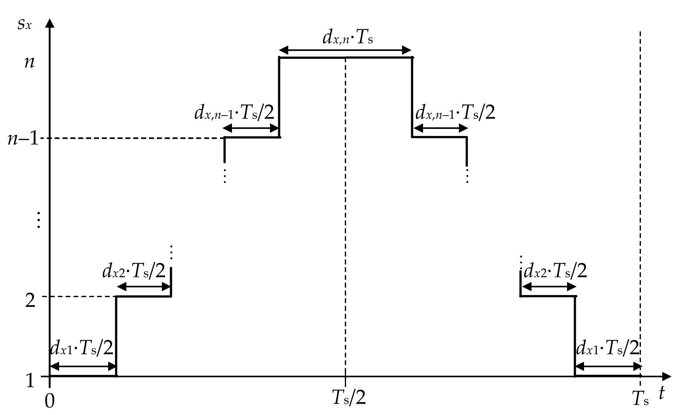
3.1. Undermodulation Range

The formulation starts with a set of three-phase modulating signals (da, db, and dc), representing a normalized value of the desired set of three-phase AC voltages from phase to load neutral (va, vb, and vc):
d a = v a v dc = m 3 · cos θ d b = v b v dc = m 3 · cos θ 2 π 3 d c = v c v dc = m 3 · cos θ 4 π 3
where θ = ω·t is the line-cycle angle.
In the second step, at each point in time, the maximum and minimum values of the modulating signals are determined:
d max = max d a , d b , d c d min = min d a , d b , d c .
In the third and final step, the duty ratios of connection of each phase x ∈ {a, b, c} to each DC-link point y ∈ {1, 2, …, n}, designated as dx,y, are calculated as
d x , 1 = d max d x d x , n = d x d min d x , k = 1 d x , 1 d x , n n 2
where k ∈ {2, 3, …, n − 1}.
This formulation can be easily extended to a case with any odd number of phases p ≥ 3, with x ∈ {1, 2, …, p}, as follows:
d x = v x v dc = m 2 · cos π 2 p · cos θ x 1 · 2 π p d max = max d 1 , d 2 , , d p d min = min d 1 , d 2 , , d p d x , 1 = d max d x d x , n = d x d min d x , k = 1 d x , 1 d x , n n 2
With the previous values of the phase duty ratios, each converter leg can be then directly controlled, applying the switching states from Table 1, in each switching cycle with period Ts, to produce the sequence of connection to the DC-link points illustrated in Figure 5.
As can be observed from Equation (4), the formulation in the undermodulation range, for any number of phases and levels, becomes extremely simple.

3.2. Full Modulation Range

If the formulation needs to cover the full range of the modulation index for a three-phase DC–AC converter, including both the undermodulation range (m ∈ [0, 1]) and the overmodulation range (m ∈ ]1, 1.1027]), then it becomes more complex. However, in the following, a fairly simple formulation is presented covering the aforementioned full modulation range, which represents the main contribution of the article.
The VVPWM strategy applied in the overmodulation range is equivalent to the strategy originally presented in [18]; i.e., it produces the same switch control signals. However, the formulation presented here is simplified. The overmodulation approach presented in [18] is composed of two substrategies or overmodulation modes: overmodulation mode I (OMI), applied for m ∈ ]1, mmaxI = 3·ln(3)/π = 1.0491], and overmodulation mode II (OMII), applied for m ∈ ]mmaxI, mmaxII = 2*sqrt(3)/π = 1.1027]. The value mmaxII corresponds to six-step operation. In addition, in [18] a reduction in the maximum modulation index value in the linear modulation range is introduced to guarantee that the duty ratio of connection to the neutral points is always higher than zero, which guarantees capacitor voltage regulation margin in every switching cycle. This reduction is introduced through the so-called hexagonal boundary compression factor hbc ∈ [0, 1], which indicates the per-unit scaling of the SVD hexagonal boundary. A value close to 1 can be typically selected.
The first proposed formulation for the full modulation range is as follows. Initially, a modified modulation index value, designated as m’, is determined, depending on the modulation region, according to the desired modulation index m, as indicated in Algorithm 1.
Algorithm 1
1: if mhbc
2:  mode = 1
3:  m’ = m
4: elseif hbc < mhbc·mmaxI
5:  mode = 1
6:   θ c = π 6 · m maxI m / h b c m maxI 1
7:   m = h b c sin θ c + π / 3
8: elseif hbc·mmaxI < mhbc·mmaxII
9:  mode = 2
10:   θ h = π 6 · m / h b c m maxI m maxII m maxI
11:   m = h b c sin θ h + π / 3
12: end
Subsequently, the phase duty ratios dx,y, x ∈ {a, b, c}, y ∈ {1, 2, …, n} can be calculated according to Algorithm 2, where med(x,y,z) outputs the medium value among variables x, y, and z; ceil(x) outputs the nearest integer above x; floor(x) outputs the nearest integer below x; and k ∈ {2, 3, …, n − 1}.
Algorithm 2
1:  d a = m 3 · cos θ
2:  d b = m 3 · cos θ 2 π 3
3:  d c = m 3 · cos θ 4 π 3
4:  d max = max d a , d b , d c
5:  d med = med d a , d b , d c
6:  d min = min d a , d b , d c
7:  d pp = d max d min
8: if dpphbc
9: if mode = 1
10:   d x , 1 = d max d x
11:   d x , n = d x d min
12: elseif mode = 2
13:  if dmed ≤ 0
14:    d x , 1 = h b c · ceil d max d x d pp
15:    d x , n = h b c · floor d x d min d pp
16:  elseif dmed > 0
17:    d x , 1 = h b c · floor d max d x d pp
18:    d x , n = h b c · ceil d x d min d pp
19:  end
20: end
21: elseif dpp > hbc
22:  d x , 1 = h b c · d max d x d pp
23:  d x , n = h b c · d x d min d pp
24: end
25: d x , k = 1 d x , 1 d x , n n 2
The combination of Algorithms 1 and 2 already provides a general and fairly simple implementation of the VVPWM including the overmodulation region. However, in Algorithm 1, the calculation of m’ involves trigonometric functions. In order to avoid the need to evaluate trigonometric functions, Algorithm 1 can be replaced by Algorithm 3.
Algorithm 3
1: if mhbc
2:  mode = 1
3:  m’ = m
4: elseif hbc < mhbc·mmaxI
5:  mode = 1
6:   m = h b c + m h b c · 2 / 3 1 m maxI 1
7: elseif hbc·mmaxI < mhbc·mmaxII
8:  mode = 2
9:   m = 2 3 · h b c m h b c · m maxI · 2 / 3 1 m maxII m maxI
10: end
The simplification in Algorithm 3 is obtained with the disadvantage of introducing some error between the achieved effective modulation index, designated as me (i.e., the modulation index calculated from the amplitude of the fundamental component of the resulting phase voltage), and the modulation index command m, in the overmodulation region. This error will be analyzed in the following section.

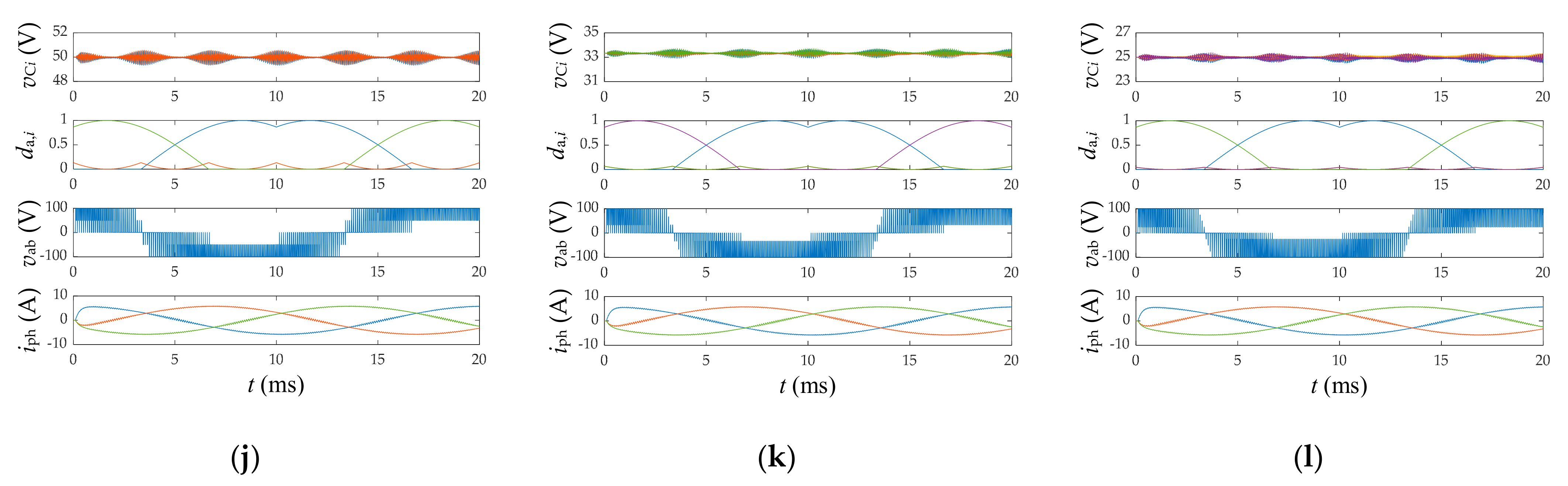
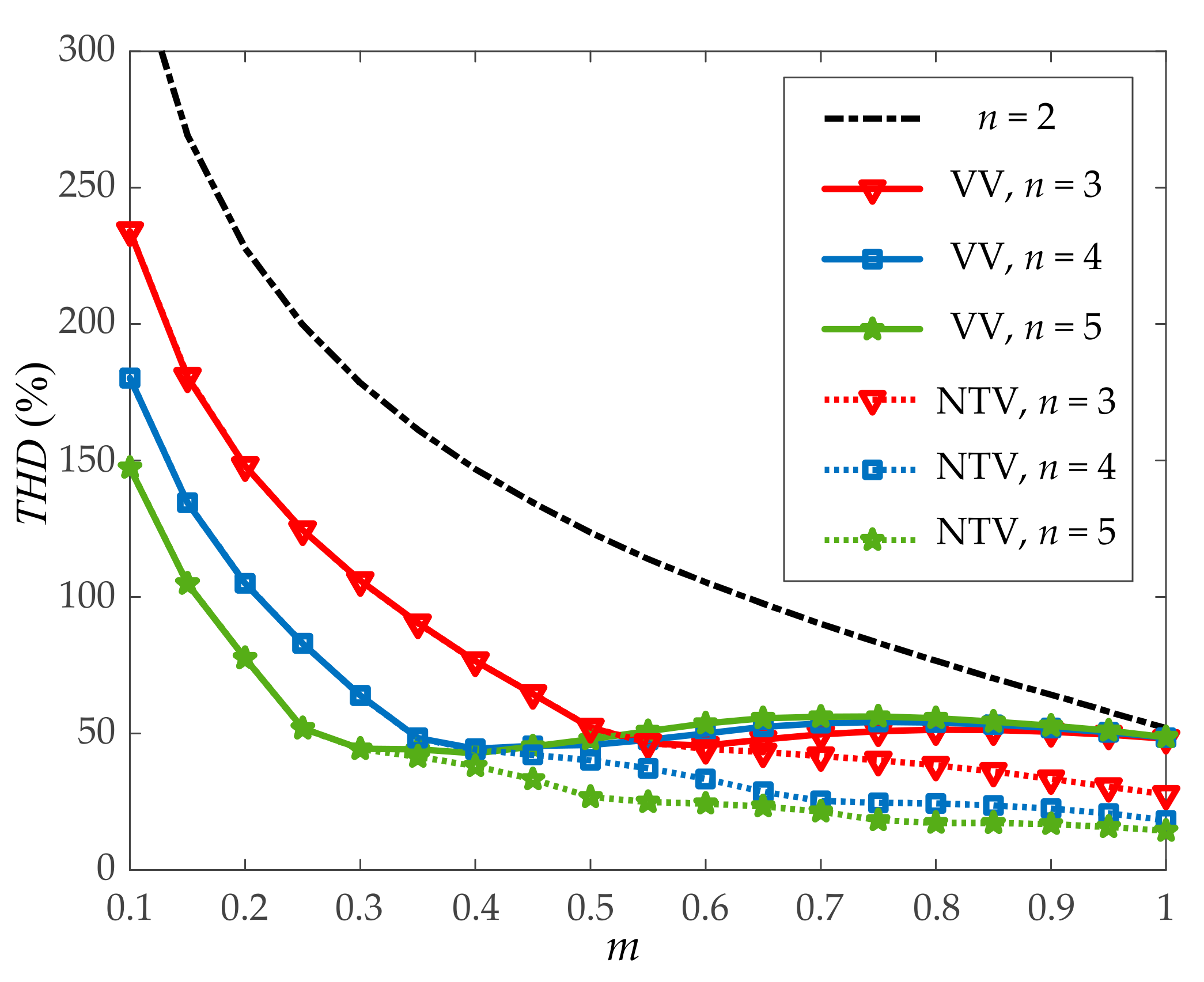
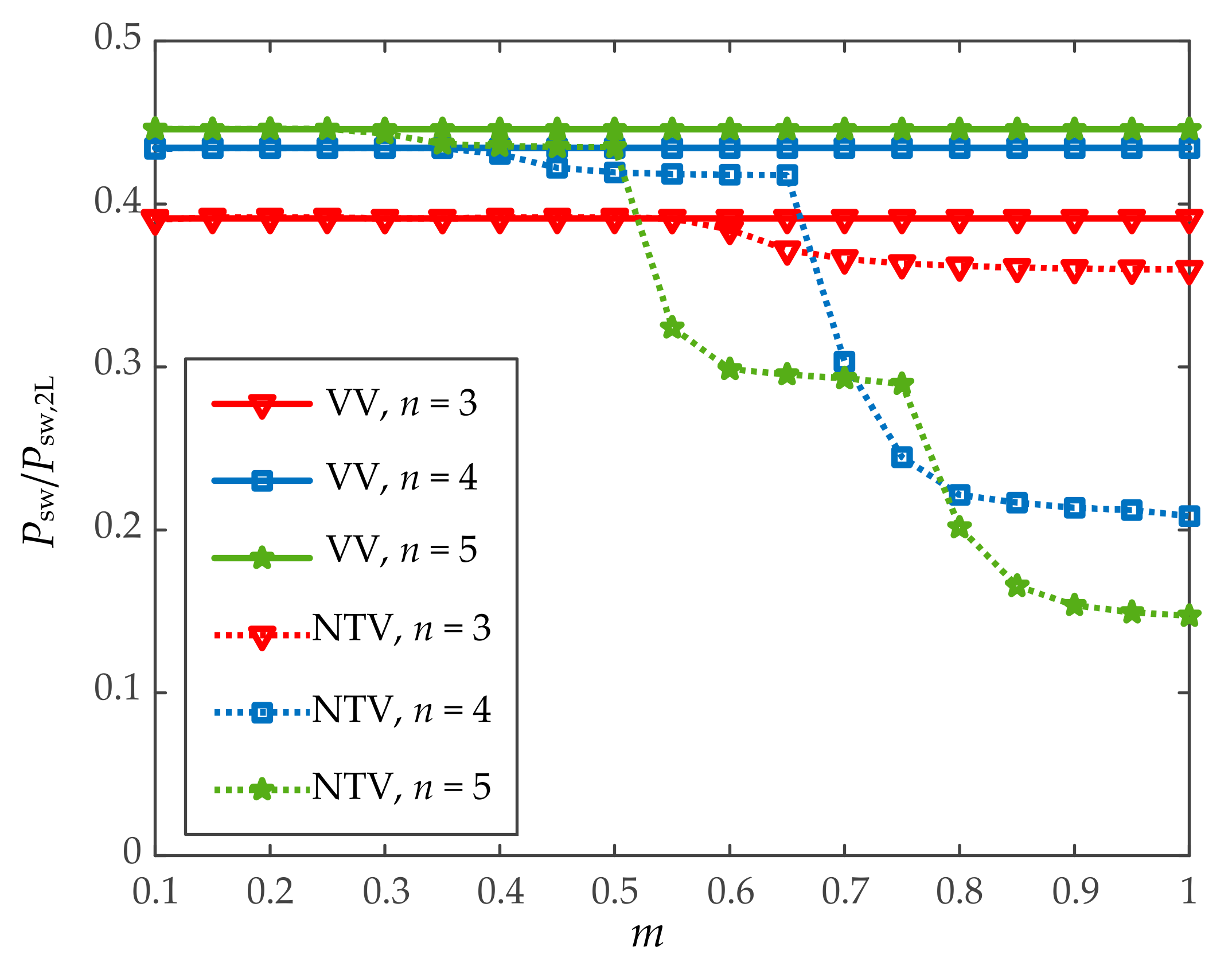
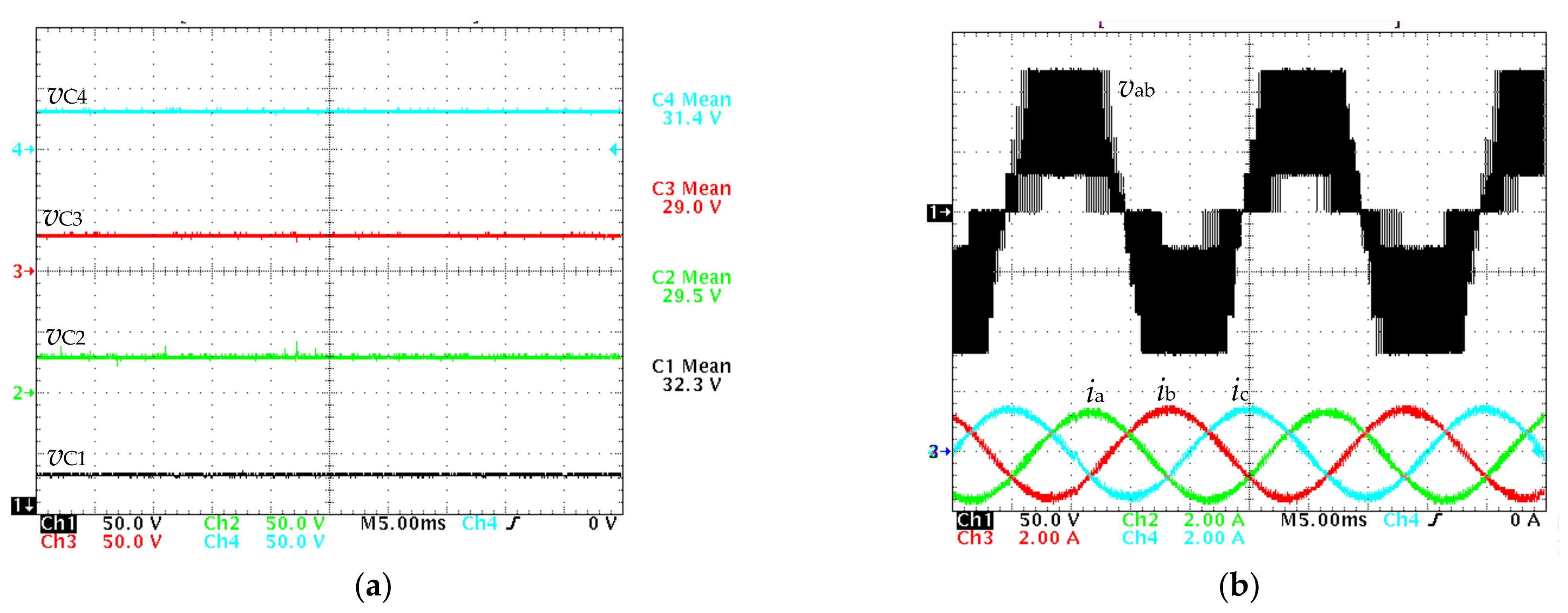
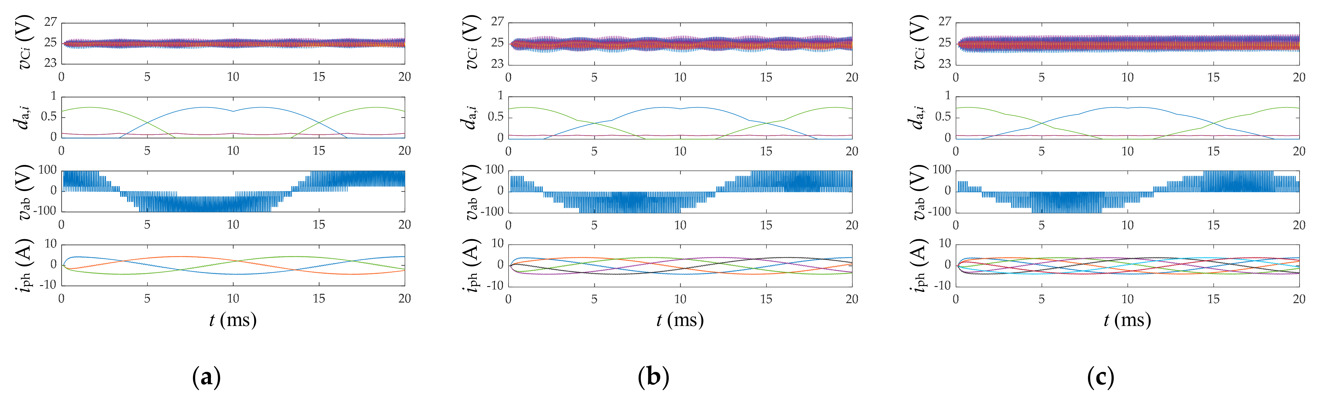
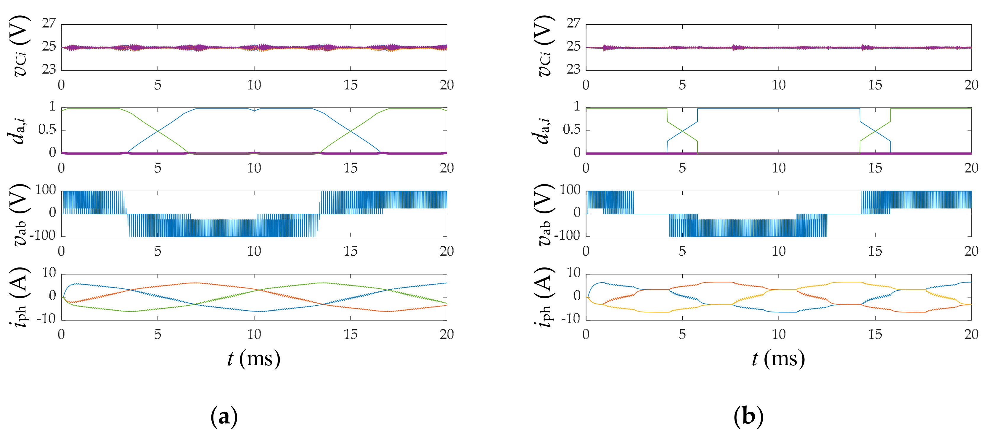
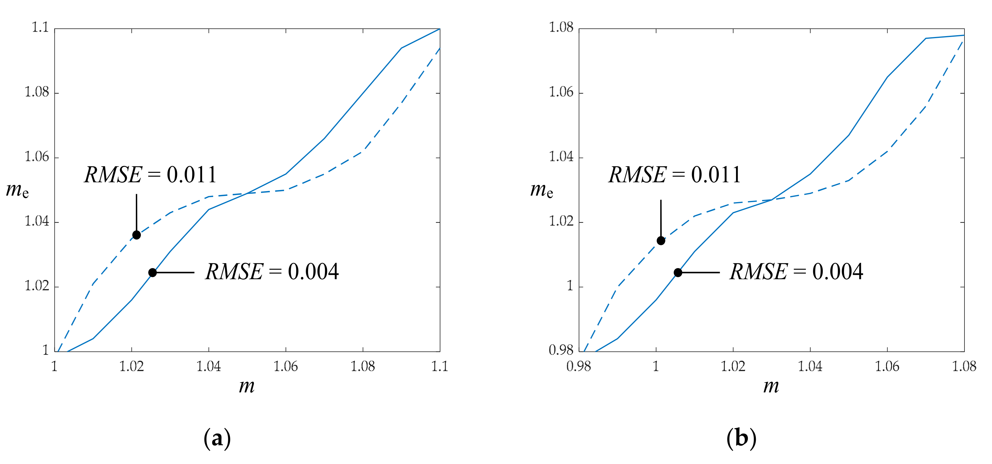
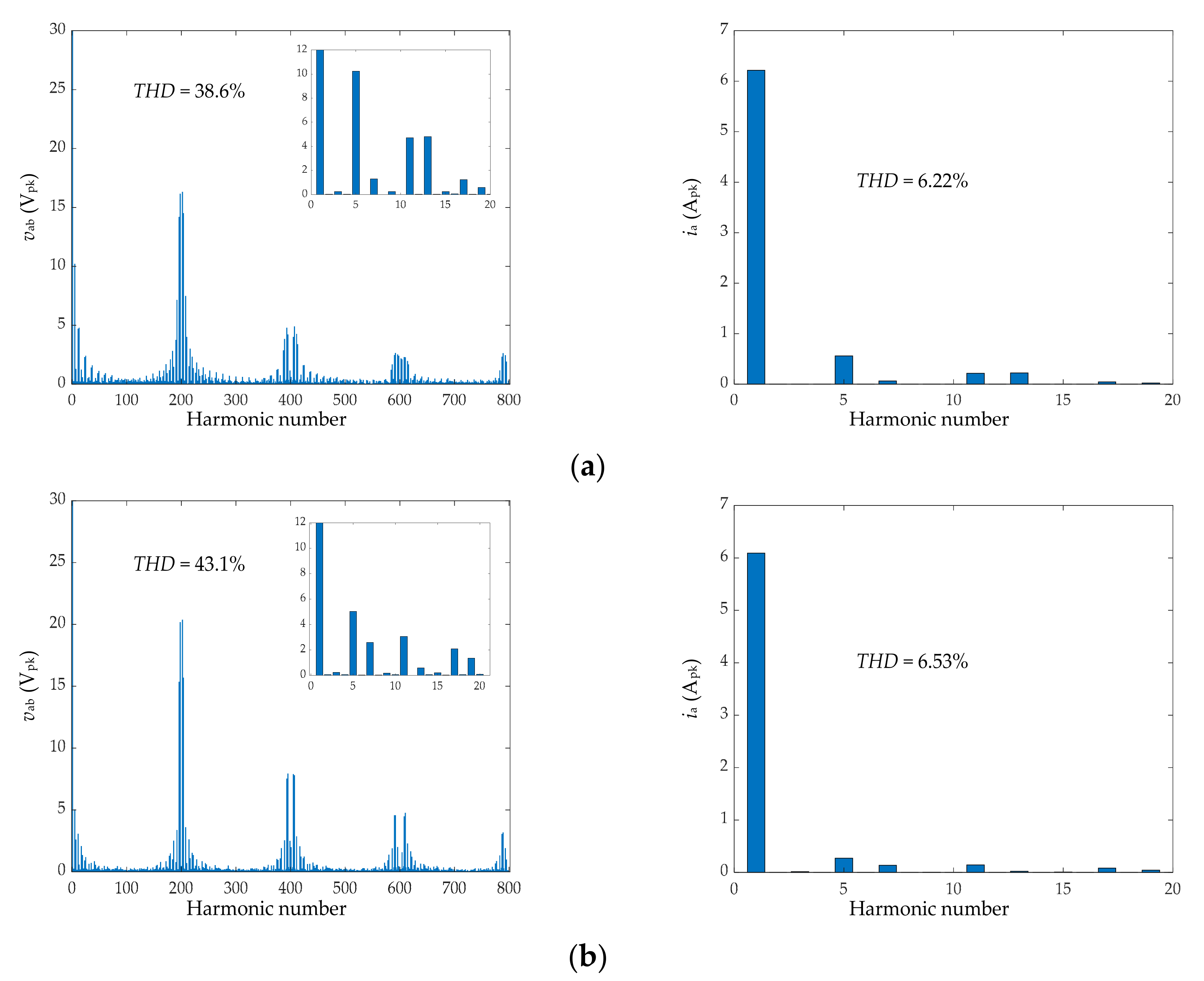
4. Simulation Results

In this section, a set of simulation results are presented to prove the good performance of the proposed formulation under a wide range of operating conditions. The system simulated is the multilevel NPC DC–AC conversion system of Figure 4, with eventually an increase in the number of phases. The DC source is assumed to be a simple DC voltage source and the AC load is assumed to be a wye-connected series resistive–inductive load. Table 2 summarizes the fixed simulation conditions.
Figure 6 illustrates the performance in the undermodulation range of a three-phase system under different modulation index values and numbers of levels. It can be observed that the phase duty ratio pattern matches the one from the original publication describing the PWM strategy [17] and that the capacitor voltages remain balanced on a per switching-cycle basis with a small capacitor voltage ripple despite the small value of the DC-link capacitance.
Using Equation (4), Figure 7 extends the application of the VVPWM strategy to a higher number of phases. As observed in Figure 7b,c, the shape of the phase duty ratios varies as the number of phases increases, showing a pattern slightly more complex than that in the three-phase case shown in Figure 7a. However, all capacitor voltages remain balanced in every switching cycle, and a proper overall performance with balanced and sinusoidal phase currents is achieved.
Figure 8 illustrates the operation in the overmodulation range, under two modulation index values corresponding to the two subregions within the overmodulation range: OMI and OMII. It can be seen that the phase duty ratios saturate in some portions of the line cycle. This is characteristic of the overmodulation region and leads to the introduction of low-order harmonics in the line-to-line voltages and phase currents. Again, the DC-link capacitor voltages remain balanced in every switching cycle.
As mentioned in Section 3, the application of the VVPWM in the full modulation range can be achieved by combining Algorithm 2 with either Algorithm 1 or Algorithm 3. Algorithm 3 is attractive since it does not involve the evaluation of trigonometric functions. However, this advantage is achieved with the drawback of worse linearity between the commanded modulation index value (m) and the effective modulation index value (me) computed from the fundamental component of the output phase voltage. This is illustrated in Figure 9 under two possible values of the hbc parameter. The root mean square error (RMSE) between me and m is indicated in Figure 9 for each curve. It can be observed that the RMSE is higher with Algorithm 3 than with Algorithm 1. However, the difference between me and m is typically lower than 2%, which should be acceptable in many applications. With reference to the case of Figure 9a, Figure 10 and Figure 11 explore the differences in line-to-line voltage and phase current harmonic distortion under two operating points where the two algorithms mostly differ: m = 1.025 and m = 1.075, respectively. Some relatively minor harmonic distortion differences can be observed, due to the different effective operating point in each case.
As mentioned in Section 1 and proved in the literature, the VVPWM achieves capacitor voltage balance in every switching cycle for any operating condition with the disadvantage of higher harmonic distortion and higher switching losses than with conventional multilevel PWM strategies. This is illustrated in Figure 12 and Figure 13, as discussed in [17]. Figure 12 compares the line-to-line voltage total harmonic distortion (THD) under the VVPWM and a conventional nearest-three-vector (NTV) PWM under different numbers of levels n. The THD value under the case of a two-level three-phase DC–AC converter is also shown as a reference for comparison. The VVPWM produces a higher THD than the NTV PWM, but the VVPWM does not require large capacitors and/or additional balancing circuitry to keep the capacitor voltages balanced, as is the case of NTV PWM. The THD values are consistently lower than those in the case of a two-level converter. Figure 13 compares the total switching power loss in per unit value of the total switching power loss of a two-level converter. As can be observed, the VVPWM produces more switching power loss than a conventional NTV PWM strategy, but the loss is smaller than that in a two-level converter. In general, conduction power loss should be similar regardless of the selected modulation strategy.
Regarding the electromagnetic interference (EMI) performance, both the differential mode noise and common-mode noise of VVPWM-operated NPC DC–AC converters are in general lower than those in the case of a two-level converter, reducing the size of the required EMI filter [35]. Nevertheless, some modulation strategy variants have been conceived to further reduce the common-mode voltage [29,32].
The satisfactory operation of multilevel NPC DC–AC converters with VVPWMs has been extensively experimentally verified in the literature [17,18,19,20,21,22,23,24,25,26,27,28,29,30,31,32,35]. Figure 14 illustrates the experimental performance of a five-level three-phase DC–AC inverter feeding a three-phase passive load under a relatively high modulation index value, for which the balancing is not possible using traditional modulation techniques.

5. Conclusions

A simple comprehensive formulation of the original VVPWM strategy for multilevel three-phase NPC DC–AC converters has been presented. The formulation is valid for any number of levels and for the full modulation range, including both the undermodulation and overmodulation regions. In the undermodulation range, it is easily extended to any number of phases. This novel formulation is directly based on basic modulating signals representing the normalized value of the desired phase-to-load-neutral voltages, with no direct reference to the SVD. Thus, it is a convenient one-stop source for researchers and practitioners looking for a general, comprehensive, and simple PWM formulation that guarantees proper performance in NPC DC–AC converters. In addition, the proposed formulation may provide additional insight into the features of VVPWM strategies, facilitate the coding and debugging of this PWM strategy, and also facilitate the development of extensions and variants.

Funding

This publication is part of Grant DPI2017-89153-P, funded by MCIN/AEI/10.13039/501100011033 and by ERDF A way of making Europe.

Conflicts of Interest

The author declares no conflict of interest. The funders had no role in the design of the study; in the collection, analyses, or interpretation of data; in the writing of the manuscript; or in the decision to publish the results.

References

  1. Levi, E. Multiphase Electric Machines for Variable-Speed Applications. IEEE Trans. Ind. Electron. 2008, 55, 1893–1909. [Google Scholar] [CrossRef]
  2. Zhu, Z.Q.; Howe, D. Electrical Machines and Drives for Electric, Hybrid, and Fuel Cell Vehicles. Proc. IEEE 2007, 95, 746–765. [Google Scholar] [CrossRef]
  3. Kouro, S.; Malinowski, M.; Gopakumar, K.; Pou, J.; Franquelo, L.G.; Wu, B.; Rodriguez, J.; Perez, M.A.; Leon, J.I. Recent Advances and Industrial Applications of Multilevel Converters. IEEE Trans. Ind. Electron. 2010, 57, 2553–2580. [Google Scholar] [CrossRef]
  4. Akagi, H. Multilevel Converters: Fundamental Circuits and Systems. Proc. IEEE 2017, 105, 2048–2065. [Google Scholar] [CrossRef]
  5. Sunddararaj, S.P.; Rangarajan, S.S.; N, S. An Extensive Review of Multilevel Inverters Based on Their Multifaceted Structural Configuration, Triggering Methods and Applications. Electronics 2020, 9, 433. [Google Scholar] [CrossRef] [Green Version]
  6. Hassan, A.; Yang, X.; Chen, W.; Houran, M.A. A State of the Art of the Multilevel Inverters with Reduced Count Components. Electronics 2020, 9, 1924. [Google Scholar] [CrossRef]
  7. Rana, R.A.; Patel, S.A.; Muthusamy, A.; Lee, C.W.; Kim, H.-J. Review of Multilevel Voltage Source Inverter Topologies and Analysis of Harmonics Distortions in FC-MLI. Electronics 2019, 8, 1329. [Google Scholar] [CrossRef] [Green Version]
  8. Rodriguez, J.; Bernet, S.; Steimer, P.K.; Lizama, I.E. A Survey on Neutral-Point-Clamped Inverters. IEEE Trans. Ind. Electron. 2010, 57, 2219–2230. [Google Scholar] [CrossRef]
  9. Busquets-Monge, S. Neutral-point-clamped dc-ac power converters. In Wiley Encyclopedia of Electrical and Electronics Engineering; Webster, J.G., Ed.; John Wiley & Sons, Inc.: Hoboken, NJ, USA, 2018; pp. 1–20. [Google Scholar]
  10. Kang, K.-P.; Cho, Y.; Kim, H.-S.; Baek, J.-W. DC-Link Capacitor Voltage Imbalance Compensation Method Based Injecting Harmonic Voltage for Cascaded Multi-Module Neutral Point Clamped Inverter. Electronics 2019, 8, 155. [Google Scholar] [CrossRef] [Green Version]
  11. Li, P.; Zhang, L.; Ouyang, B.; Liu, Y. Nonlinear Effects of Three-Level Neutral-Point Clamped Inverter on Speed Sensorless Control of Induction Motor. Electronics 2019, 8, 402. [Google Scholar] [CrossRef] [Green Version]
  12. Kim, S.-H.; Kim, S.-M.; Park, S.; Lee, K.-B. Switch Open-Fault Detection for a Three-Phase Hybrid Active Neutral-Point-Clamped Rectifier. Electronics 2020, 9, 1437. [Google Scholar] [CrossRef]
  13. Halabi, L.M.; Alsofyani, I.M.; Lee, K.-B. Open-Circuit Fault Tolerance Method for Three-Level Hybrid Active Neutral Point Clamped Converters. Electronics 2020, 9, 1535. [Google Scholar] [CrossRef]
  14. Madasamy, P.; Verma, R.; Rameshbabu, A.; Murugesan, A.; Umamageswari, R.; Munda, J.; Bharatiraja, C.; Mihet-Popa, L. Neutral Point Clamped Transformer-Less Multilevel Converter for Grid-Connected Photovoltaic System. Electronics 2021, 10, 977. [Google Scholar] [CrossRef]
  15. Barros, J.; Rocha, L.; Silva, J. Backstepping Predictive Control of Hybrid Microgrids Interconnected by Neutral Point Clamped Converters. Electronics 2021, 10, 1210. [Google Scholar] [CrossRef]
  16. Alepuz, S.; Busquets-Monge, S.; Nicolás-Apruzzese, J.; Filbà-Martínez, À.; Bordonau, J.; Yuan, X.; Kouro, S. A Survey on Capacitor Voltage Control in Neutral-Point-Clamped Multilevel Converters. Electronics 2022, 11, 527. [Google Scholar] [CrossRef]
  17. Busquets-Monge, S.; Alepuz, S.; Rocabert, J.; Bordonau, J. Pulsewidth Modulations for the Comprehensive Capacitor Voltage Balance of n-Level Three-Leg Diode-Clamped Converters. IEEE Trans. Power Electron. 2009, 24, 1364–1375. [Google Scholar] [CrossRef] [Green Version]
  18. Busquets-Monge, S.; Maheshwari, R.; Munk-Nielsen, S. Overmodulation of n-Level Three-Leg DC–AC Diode-Clamped Converters with Comprehensive Capacitor Voltage Balance. IEEE Trans. Ind. Electron. 2012, 60, 1872–1883. [Google Scholar] [CrossRef]
  19. Busquets-Monge, S.; Ruderman, A. Carrier-based PWM strategies for the comprehensive capacitor voltage balance of mul-tilevel multileg diode-clamped converters. In Proceedings of the 2010 IEEE International Symposium on Industrial Electronics, Bari, Italy, 4–7 July 2010. [Google Scholar]
  20. Maheshwari, R.; Munk-Nielsen, S.; Busquets-Monge, S. A carrier-based approach for overmodulation of three-level neutral-point-clamped inverter with zero neutral-point current. In Proceedings of the 2012 IEEE Energy Conversion Congress and Exposition (ECCE), Raleigh, NC, USA, 15–20 September 2012; pp. 1767–1773. [Google Scholar]
  21. Gui, S.W.; Lin, Z.J.; Huang, S.H. A Varied VSVM Strategy for Balancing the Neutral-Point Voltage of DC-Link Capacitors in Three-Level NPC Converters. Energies 2015, 8, 2032–2047. [Google Scholar] [CrossRef] [Green Version]
  22. Hu, C.; Yu, X.; Holmes, D.G.; Shen, W.; Wang, Q.; Luo, F.; Liu, N. An Improved Virtual Space Vector Modulation Scheme for Three-Level Active Neutral-Point-Clamped Inverter. IEEE Trans. Power Electron. 2016, 32, 7419–7434. [Google Scholar] [CrossRef]
  23. Wang, J.; Gao, Y.; Jiang, W.; Weidong, J. A Carrier-Based Implementation of Virtual Space Vector Modulation for Neutral-Point-Clamped Three-Level Inverter. IEEE Trans. Ind. Electron. 2017, 64, 9580–9586. [Google Scholar] [CrossRef]
  24. Wu, X.; Tan, G.; Ye, Z.; Yao, G.; Liu, Z.; Liu, G. Virtual-Space-Vector PWM for a Three-Level Neutral-Point-Clamped Inverter with Unbalanced DC-Links. IEEE Trans. Power Electron. 2017, 33, 2630–2642. [Google Scholar] [CrossRef]
  25. Xiang, C.-Q.; Shu, C.; Han, D.; Mao, B.-K.; Wu, X.; Yu, T.-J. Improved Virtual Space Vector Modulation for Three-Level Neutral-Point-Clamped Converter with Feedback of Neutral-Point Voltage. IEEE Trans. Power Electron. 2018, 33, 5452–5464. [Google Scholar] [CrossRef]
  26. Liu, G.; Wang, D.; Wang, M.; Zhu, C.; Wang, M. Neutral-Point Voltage Balancing in Three-Level Inverters Using an Optimized Virtual Space Vector PWM with Reduced Commutations. IEEE Trans. Ind. Electron. 2018, 65, 6959–6969. [Google Scholar] [CrossRef]
  27. Weidong, J.; Wang, L.; Wang, J.; Zhang, X.; Wang, P. A Carrier-Based Virtual Space Vector Modulation With Active Neutral-Point Voltage Control for a Neutral-Point-Clamped Three-Level Inverter. IEEE Trans. Ind. Electron. 2018, 65, 8687–8696. [Google Scholar] [CrossRef]
  28. Giri, S.K.; Mukherjee, S.; Kundu, S.; Banerjee, S.; Chakraborty, C. An Improved PWM Scheme for Three-Level Inverter Extending Operation into Overmodulation Region with Neutral-Point Voltage Balancing for Full Power-Factor Range. IEEE J. Emerg. Sel. Top. Power Electron. 2018, 6, 1527–1539. [Google Scholar] [CrossRef]
  29. Jiang, W.; Wang, P.; Ma, M.; Wang, J.; Li, J.; Li, L.; Chen, K.; Weidong, J. A Novel Virtual Space Vector Modulation with Reduced Common-Mode Voltage and Eliminated Neutral Point Voltage Oscillation for Neutral Point Clamped Three-Level Inverter. IEEE Trans. Ind. Electron. 2019, 67, 884–894. [Google Scholar] [CrossRef]
  30. Qamar, M.A.; Wang, K.; Zheng, Z.; Wang, S.; Li, Y. A Simplified Virtual Vector PWM Algorithm to Balance the Capacitor Voltages of Four-Level Diode-Clamped Converter. IEEE Access 2020, 8, 180896–180908. [Google Scholar] [CrossRef]
  31. Guo, F.; Yang, T.; Diab, A.M.; Yeoh, S.S.; Bozhko, S.; Wheeler, P. An Enhanced Virtual Space Vector Modulation Scheme of Three-Level NPC Converters for More-Electric-Aircraft Applications. IEEE Trans. Ind. Appl. 2021, 57, 5239–5251. [Google Scholar] [CrossRef]
  32. Xia, S.; Wu, X.; Zheng, J.; Li, X.; Wang, K. A Virtual Space Vector PWM With Active Neutral Point Voltage Control and Common Mode Voltage Suppression for Three-Level NPC Converters. IEEE Trans. Ind. Electron. 2021, 68, 11761–11771. [Google Scholar] [CrossRef]
  33. Wang, K.; Zheng, Z.; Li, Y. A Novel Carrier-Overlapped PWM Method for Four-Level Neutral-Point Clamped Converters. IEEE Trans. Power Electron. 2019, 34, 7–12. [Google Scholar] [CrossRef]
  34. Wang, J.; Wang, J.; Xiao, B.; Gui, Z.; Jiang, W. Full Range Capacitor Voltage Balance PWM Strategy for Diode-Clamped Multilevel Inverter. Electronics 2020, 9, 1263. [Google Scholar] [CrossRef]
  35. Maheshwari, R.; Munk-Nielsen, S.; Busquets-Monge, S. EMI performance comparison of two-level and three-level inverters in small dc-link capacitors based motor drives. In Proceedings of the 2012 IEEE International Symposium on Industrial Electronics, Hangzhou, China, 28–31 May 2012; pp. 652–657. [Google Scholar]
Figure 1. Three-phase motor drives. (a) Conventional two-level converter; (b) three-level diode-clamped NPC converter.
Electronics 11 00641 g001
Figure 2. Functional model of an n-level NPC converter leg. The single-pole n-throw switch is represented with two alternative symbols.
Electronics 11 00641 g002
Figure 3. NPC leg topologies [9]. (a) Active NPC (ANPC); (b) passive NPC (PNPC); (c) reduced ANPC; (d) reduced PNPC.
Electronics 11 00641 g003
Figure 4. Multilevel three-phase NPC DC–AC conversion system.
Electronics 11 00641 g004
Figure 5. Sequence of connection of each leg to the DC-link points over a switching cycle.
Electronics 11 00641 g005
Figure 6. Simulation results for the three-phase NPC DC–AC conversion system of Figure 4, operated with the proposed VVPWM strategy formulation, under different modulation index values m and numbers of levels n in the undermodulation range (hbc = 1). (a) m = 0.25, n = 3; (b) m = 0.25, n = 4; (c) m = 0.25, n = 5; (d) m = 0.5, n = 3; (e) m = 0.5, n = 4; (f) m = 0.5, n = 5; (g) m = 0.75, n = 3; (h) m = 0.75, n = 4; (i) m = 0.75, n = 5; (j) m = 1, n = 3; (k) m = 1, n = 4; (l) m = 1, n = 5.
Electronics 11 00641 g006aElectronics 11 00641 g006b
Figure 7. Simulation results for an NPC DC–AC conversion system, operated with the proposed VVPWM strategy formulation, under m = 0.75, n = 5, and different numbers of phases. (a) Three phases; (b) five phases; (c) seven phases.
Electronics 11 00641 g007
Figure 8. Simulation results for the three-phase NPC DC–AC conversion system of Figure 4, with n = 5, operated with the proposed VVPWM strategy formulation and hbc = 0.98, under two different modulation index values m corresponding to the overmodulation region. (a) m = 1.01 (OMI); (b) m = 1.07 (OMII).
Electronics 11 00641 g008
Figure 9. Effective modulation index (me) as a function of the commanded modulation index (m) in the overmodulation region for two cases: algorithm implemented with Algorithms 1 and 2 (solid line) and algorithm implemented with Algorithms 2 and 3 (dashed line). (a) hbc = 1; (b) hbc = 0.98.
Electronics 11 00641 g009
Figure 10. Line-to-line voltage and phase current harmonic distortion under m = 1.025 and hbc = 1. (a) Algorithm implemented with Algorithms 1 and 2; (b) algorithm implemented with Algorithms 2 and 3.
Electronics 11 00641 g010
Figure 11. Line-to-line voltage and phase current harmonic distortion under m = 1.075 and hbc = 1. (a) Algorithm implemented with Algorithms 1 and 2; (b) algorithm implemented with Algorithms 2 and 3.
Electronics 11 00641 g011
Figure 12. Total harmonic distortion of the line-to-line voltage in a three-phase multilevel NPC DC–AC converter operated with the VVPWM and operated with a reference NTV PWM [17].
Electronics 11 00641 g012
Figure 13. Switching power loss in a three-phase multilevel NPC DC–AC converter operated with the VVPWM and operated with a reference NTV PWM in per unit value of the switching power loss of a two-level converter [17].
Electronics 11 00641 g013
Figure 14. Experimental results of a five-level three-phase DC–AC converter operated with VVPWM under the following conditions: Vdc = 120 V, m = 0.75, C = 155 μF, fs = 5 kHz, and a linear and balanced load with per-phase impedance ZL = 33.5 Ω ∠8.5° (series R-L load) [17]. (a) DC-link capacitor voltages; (b) Line-to-line voltage and phase currents.
Electronics 11 00641 g014
Table 1. NPC leg switching states [9].
sacConnection of AC Terminal tos1s2s3sk−1sksn−3sn−2sn−1
1dc100000000
2dc210000000
3dc311000000
kdck11110000
n − 2dcn−211111100
n − 1dcn−111111110
ndcn11111111
Table 2. Simulation conditions.
ParameterDescriptionValue
VdcTotal DC-link voltage100 V
CCapacitance of each DC-link capacitor100 µF
foLine-cycle fundamental frequency50 Hz
fsSwitching frequency10 kHz
RLPer-phase load resistance10 Ω
LLPer-phase load inductance2 mH
Publisher’s Note: MDPI stays neutral with regard to jurisdictional claims in published maps and institutional affiliations.

