
Cascaded-like High-Step-Down Converter with Single Switch and Leakage Energy Recycling in Single-Stage Structure


Abstract
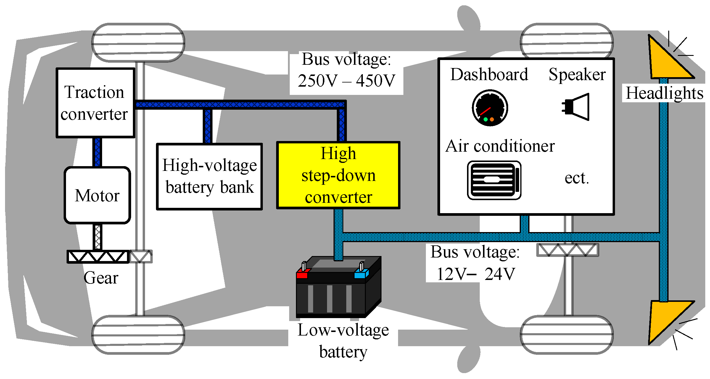
:1. Introduction
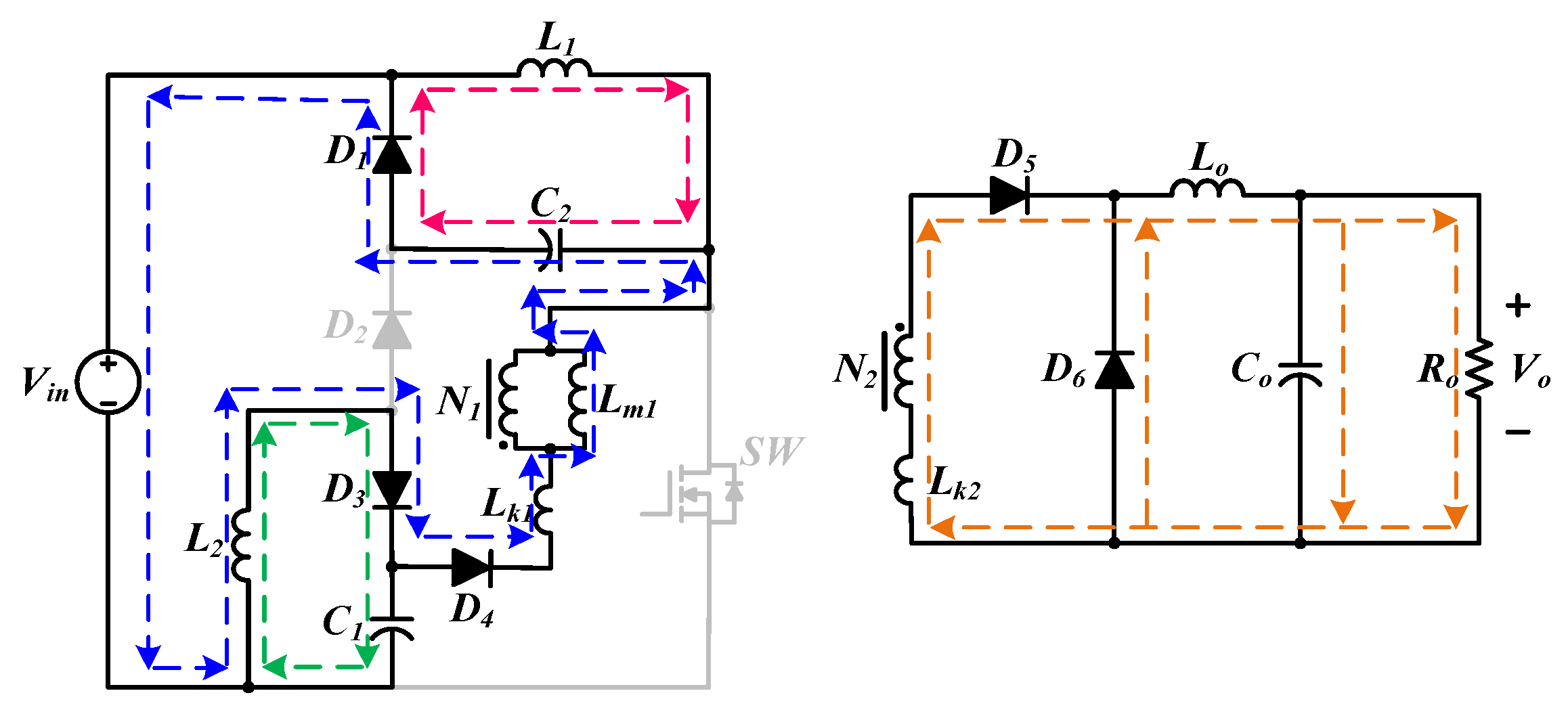
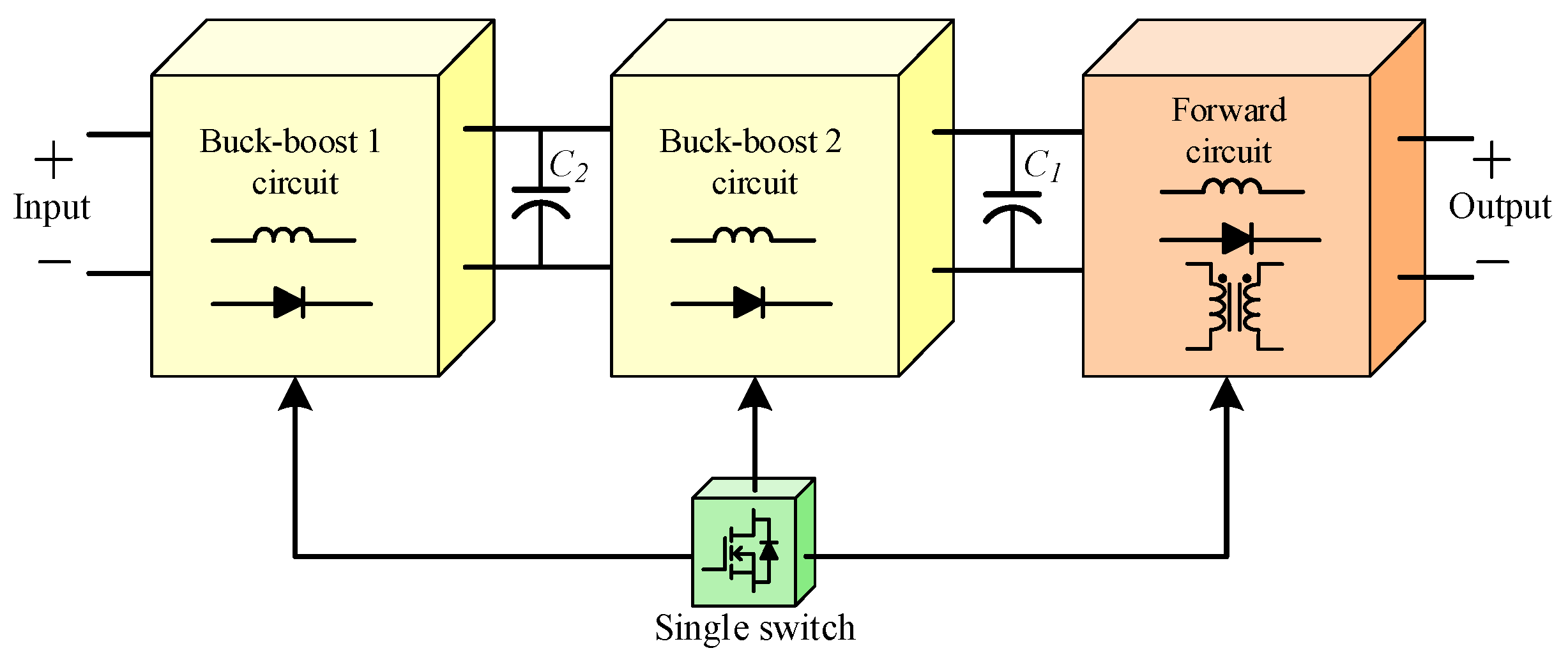
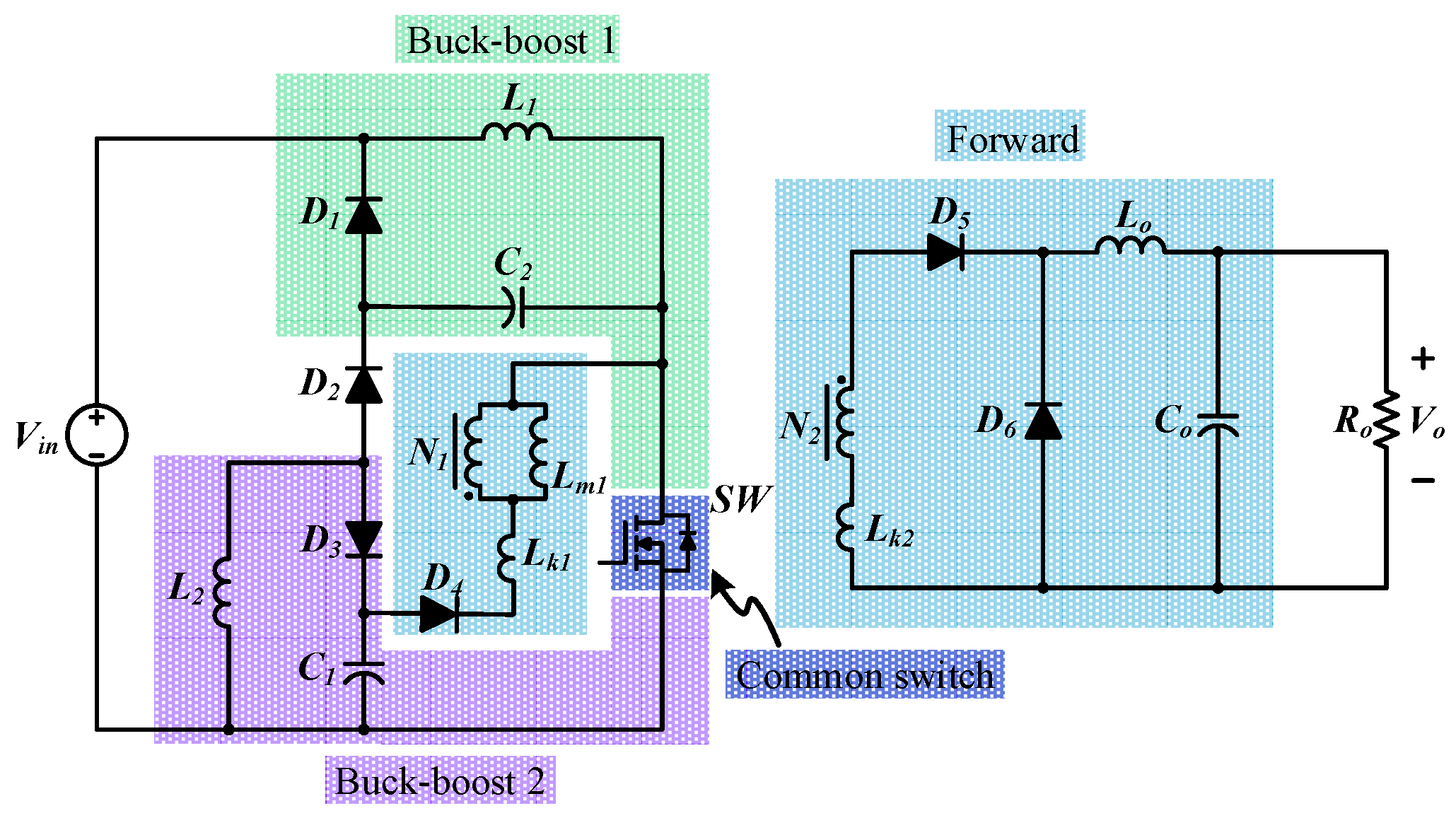
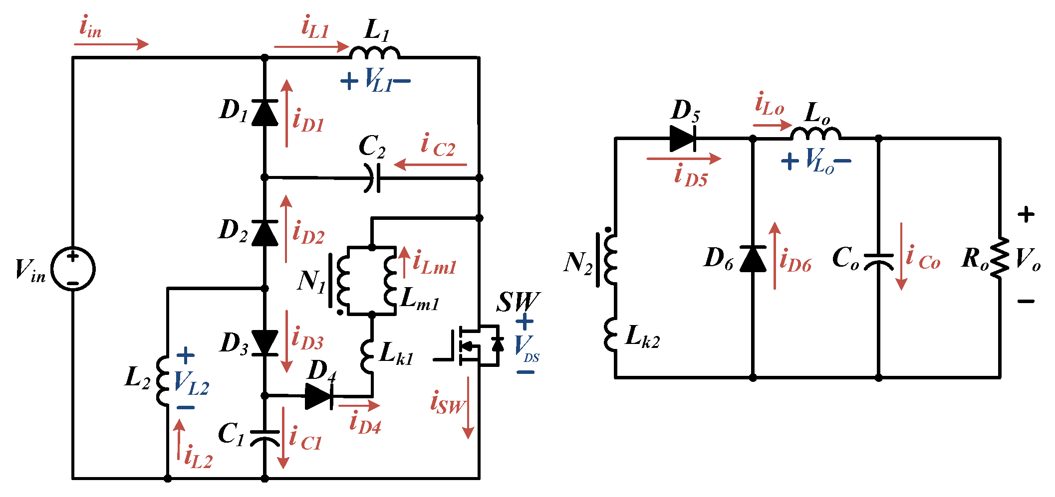
2. Converter Structure and Operation Principle
- All the capacitors are large enough so that the voltages across them are regarded as constant and ripple-free;
- All semiconductor devices and diodes are ideal. That is, parasitic parameters can be neglected;
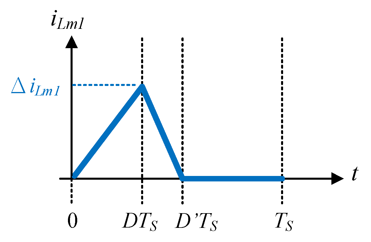
- The Lk1 and Lk2 represent the leakage inductances at the primary side and secondary side of the high-frequency transformer, respectively, values of which both are much smaller than the magnetizing inductance Lm1;
- The duty ratio of the switch SW will be less than 0.5;
- The turns ratio of the coupled inductor n is equal to ;
- The inductors L1 and L2 in the buck-boost circuits and the inductor Lo in the forward circuit all operate in continuous conduction mode (CCM).
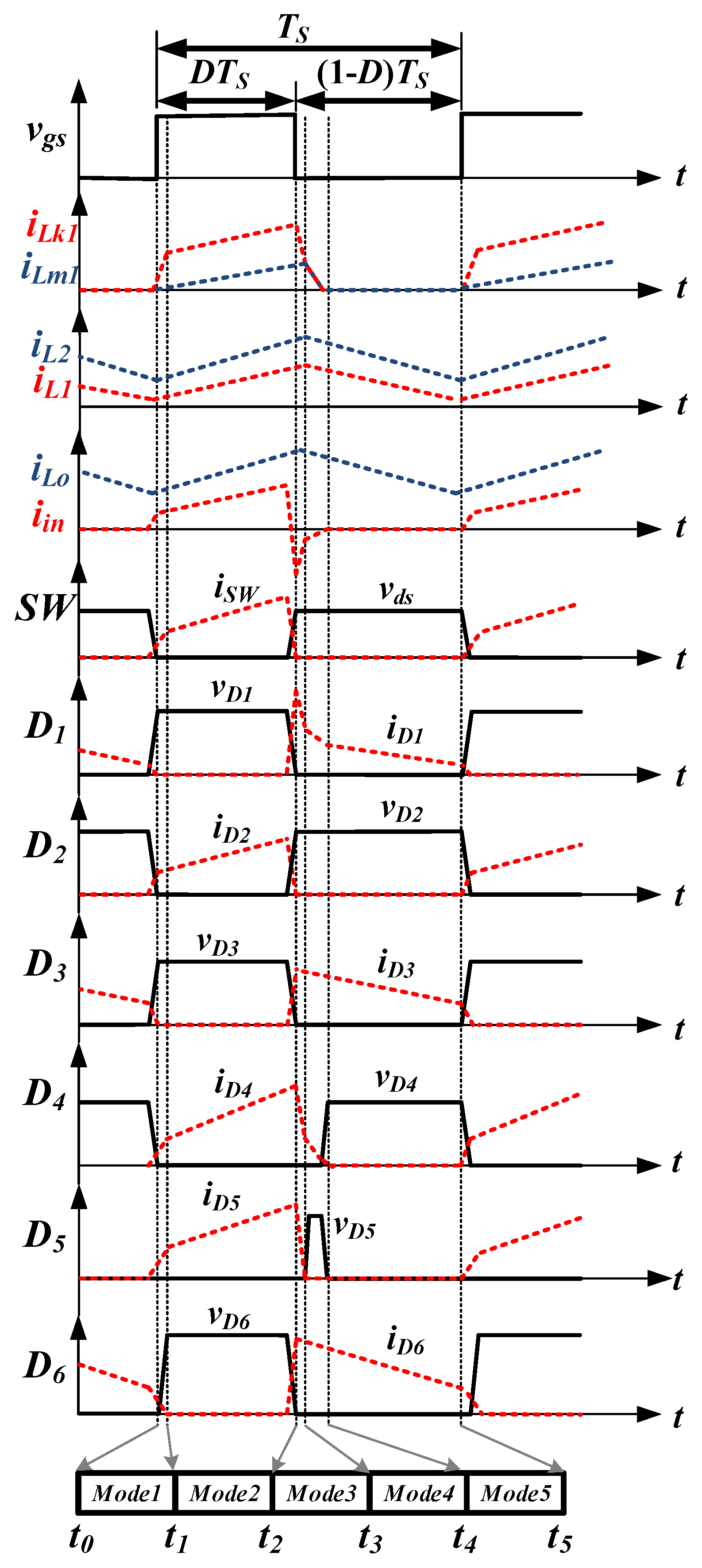
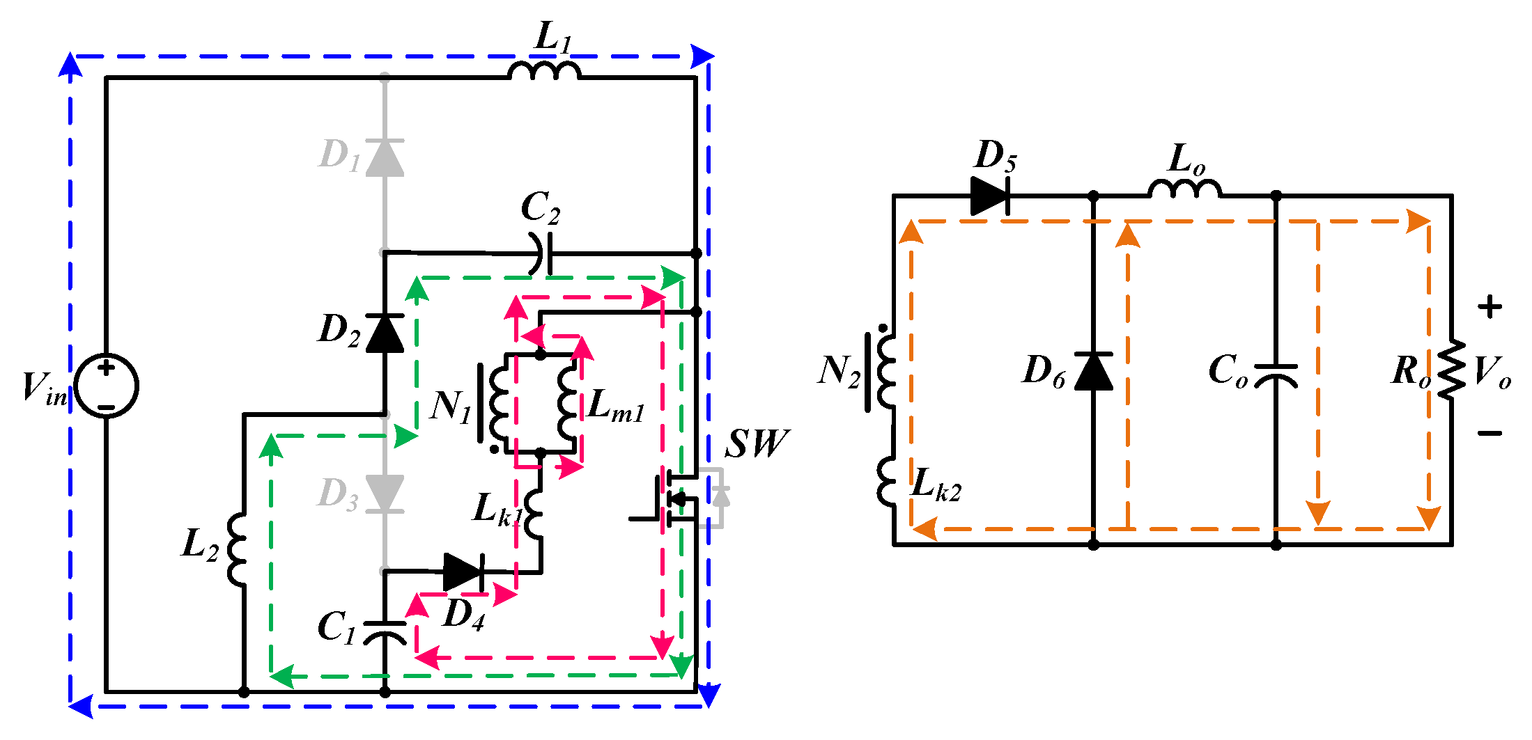
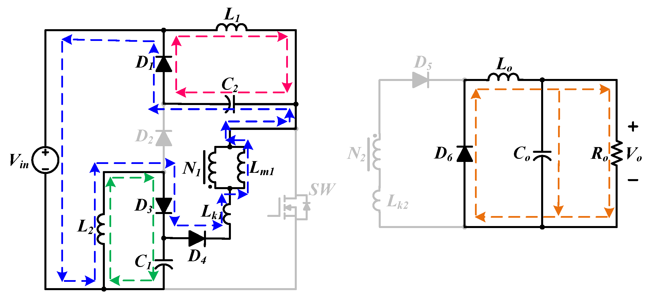
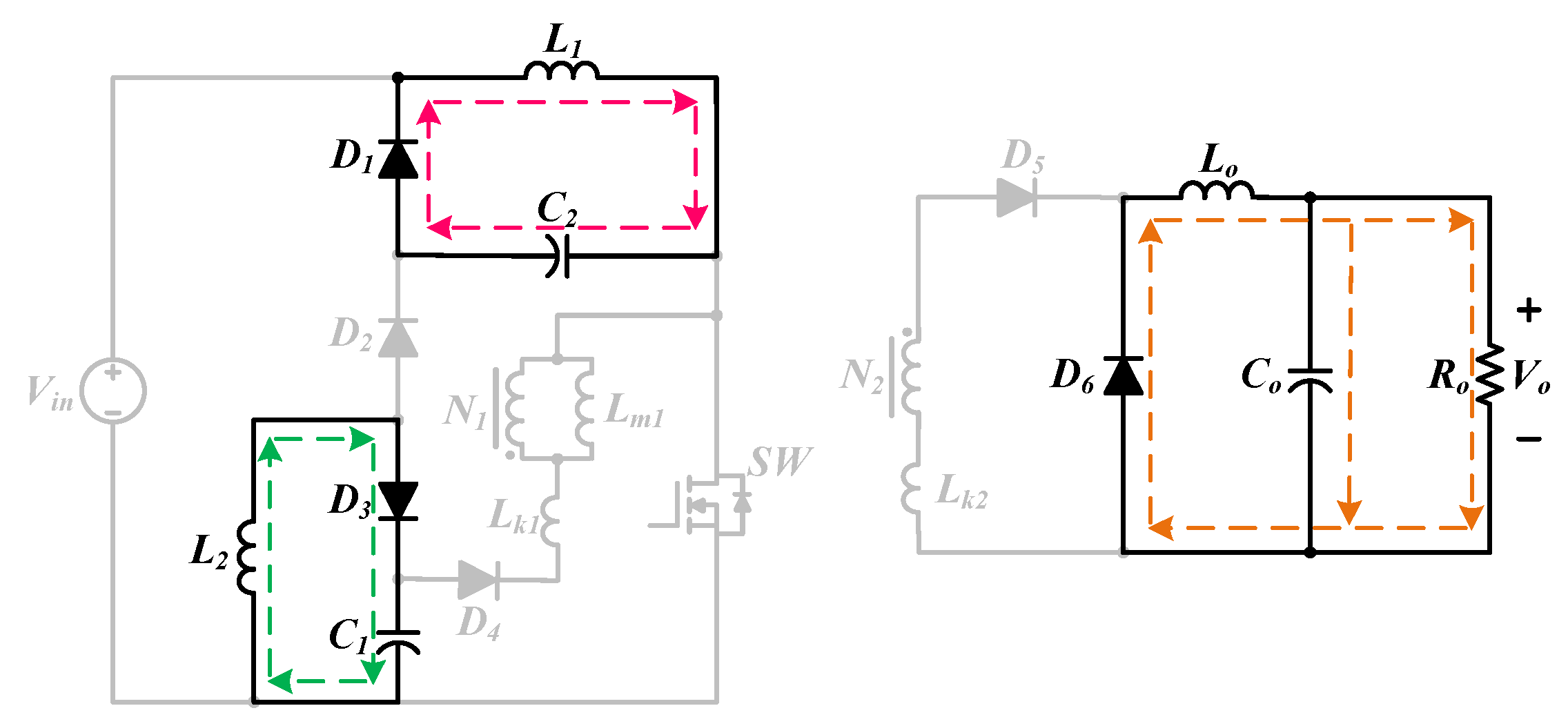
- Mode 1 [t0~t1]:
- Mode 2 [t1~t2]:
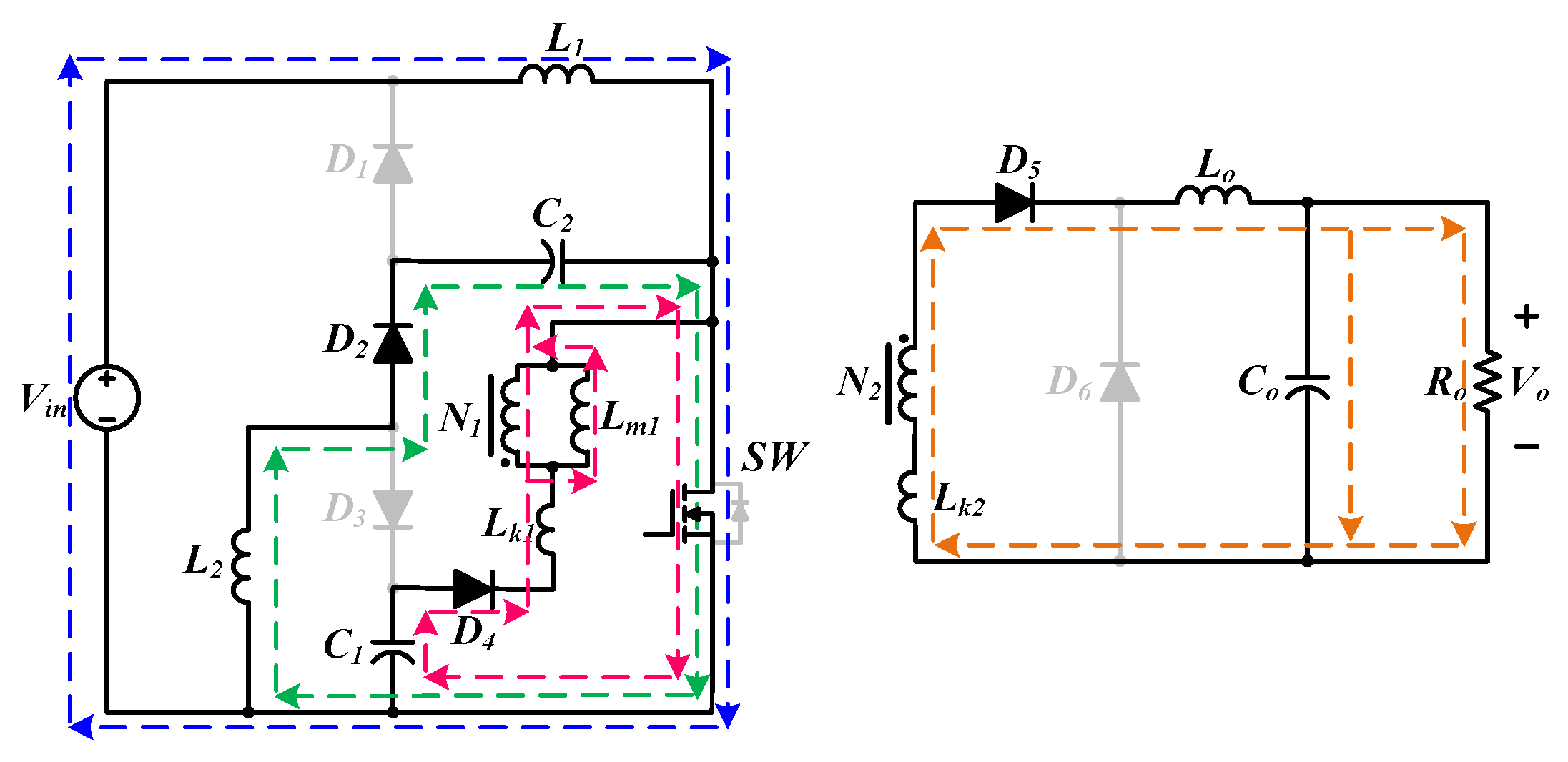
- Mode 3 [t2~t3]:
- Mode 4 [t3~t4]:
- Mode 5 [t4~t5]:
3. Steady-State Analysis
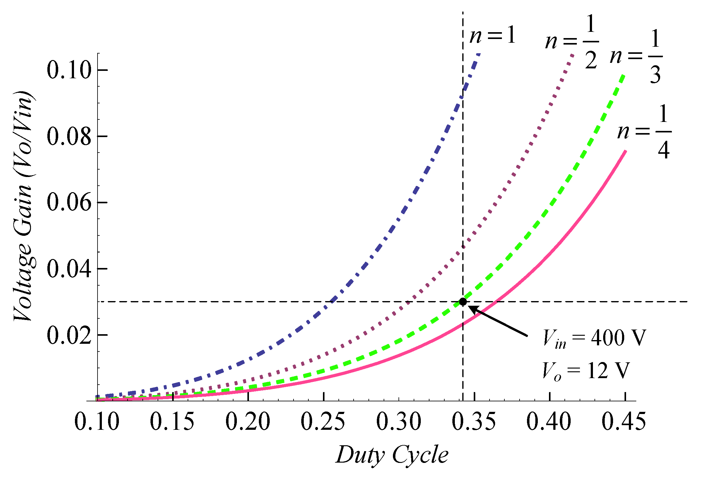
3.1. Voltage Gain
3.2. Voltage Stresses of Semiconductors
3.3. Current Stresses of Semiconductors
3.4. Inductance Design
3.5. Capacitance Design
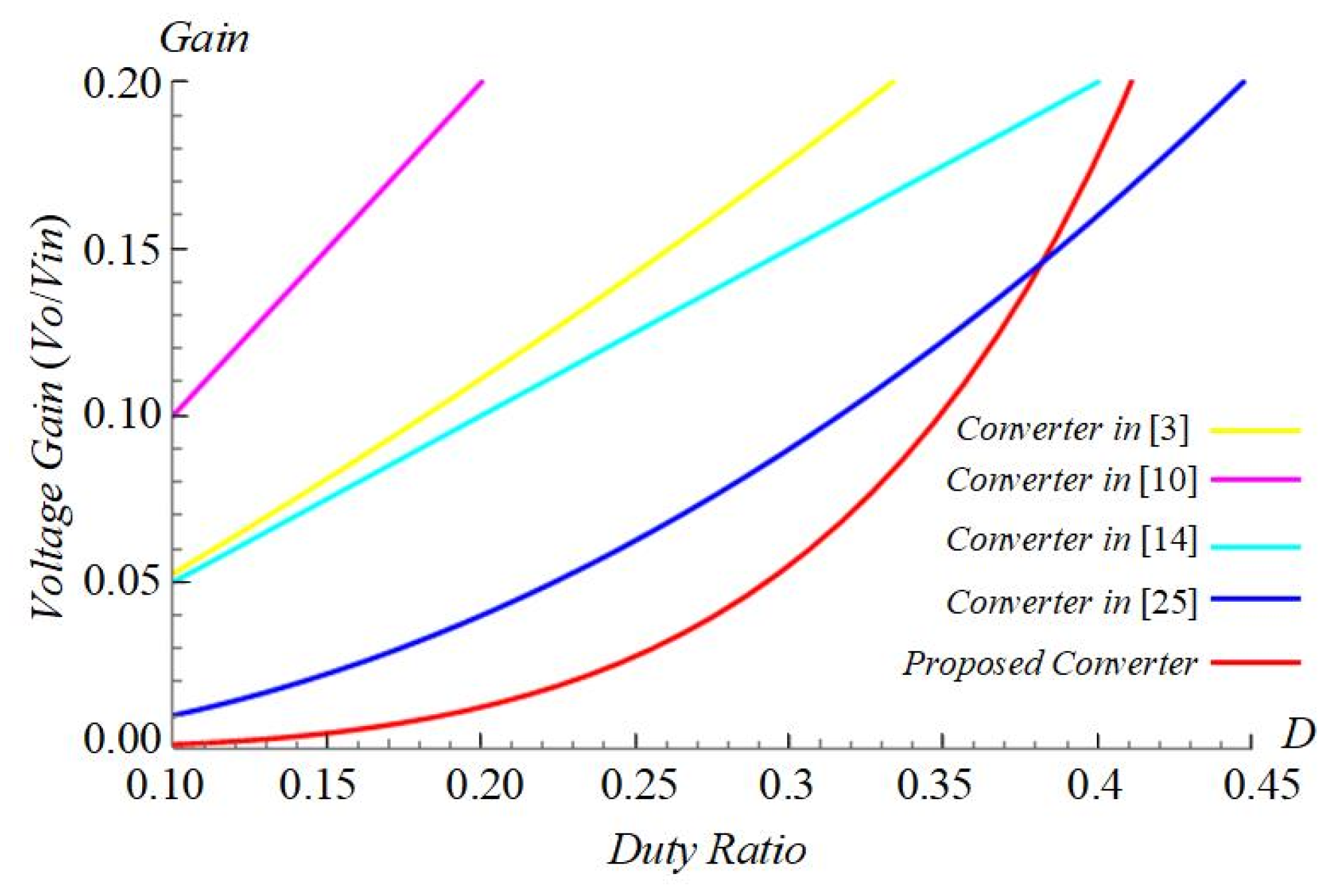
3.6. Performance Comparison
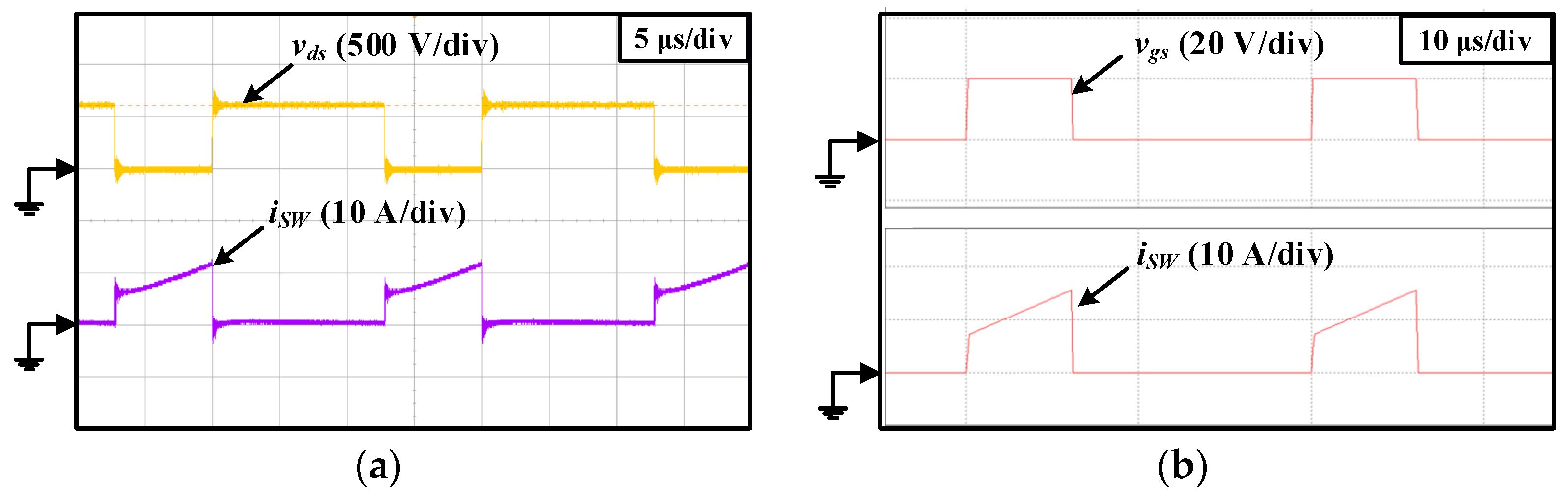
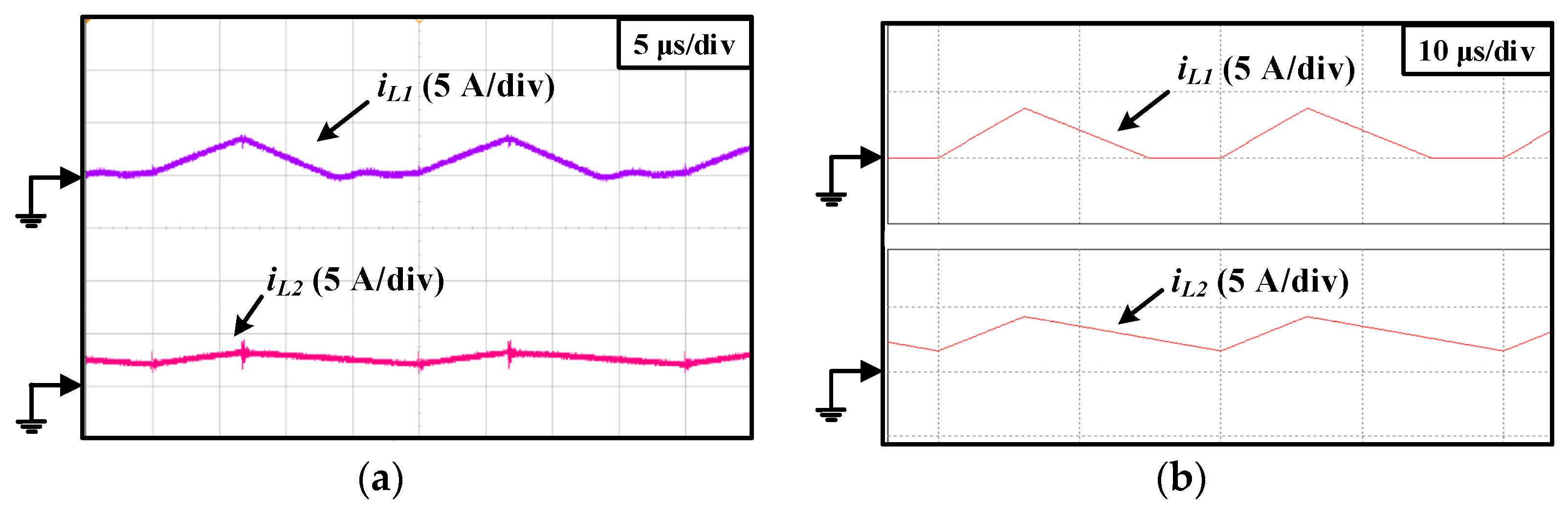
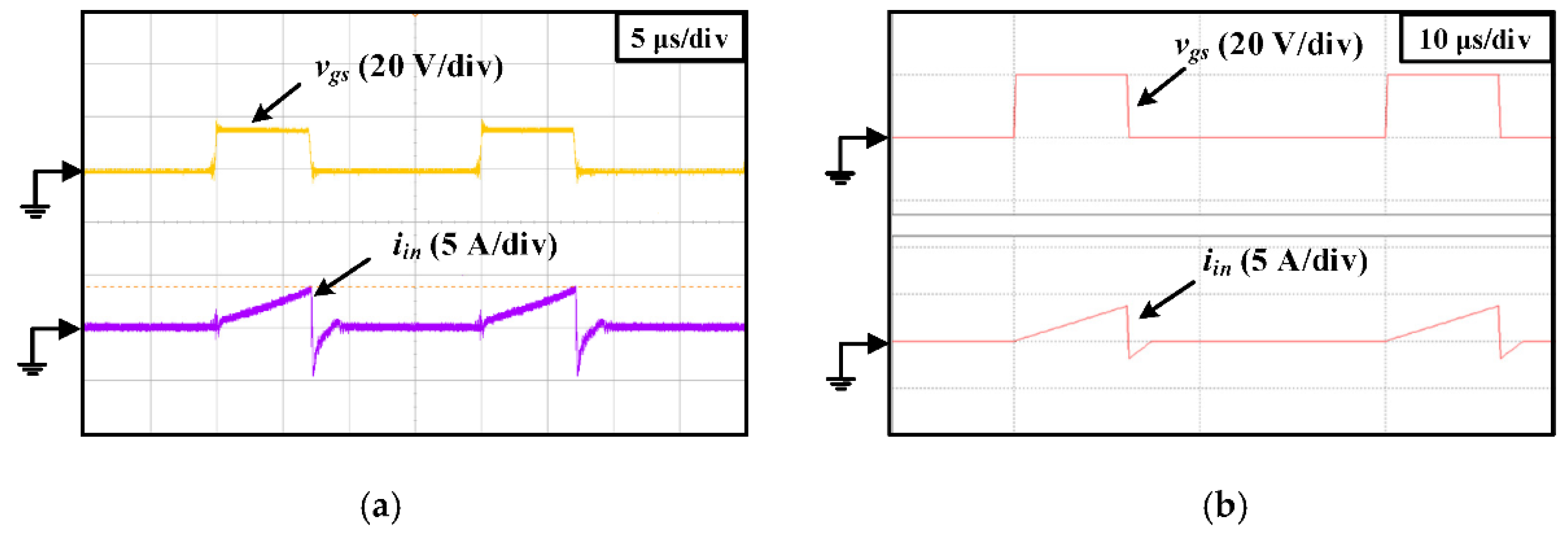
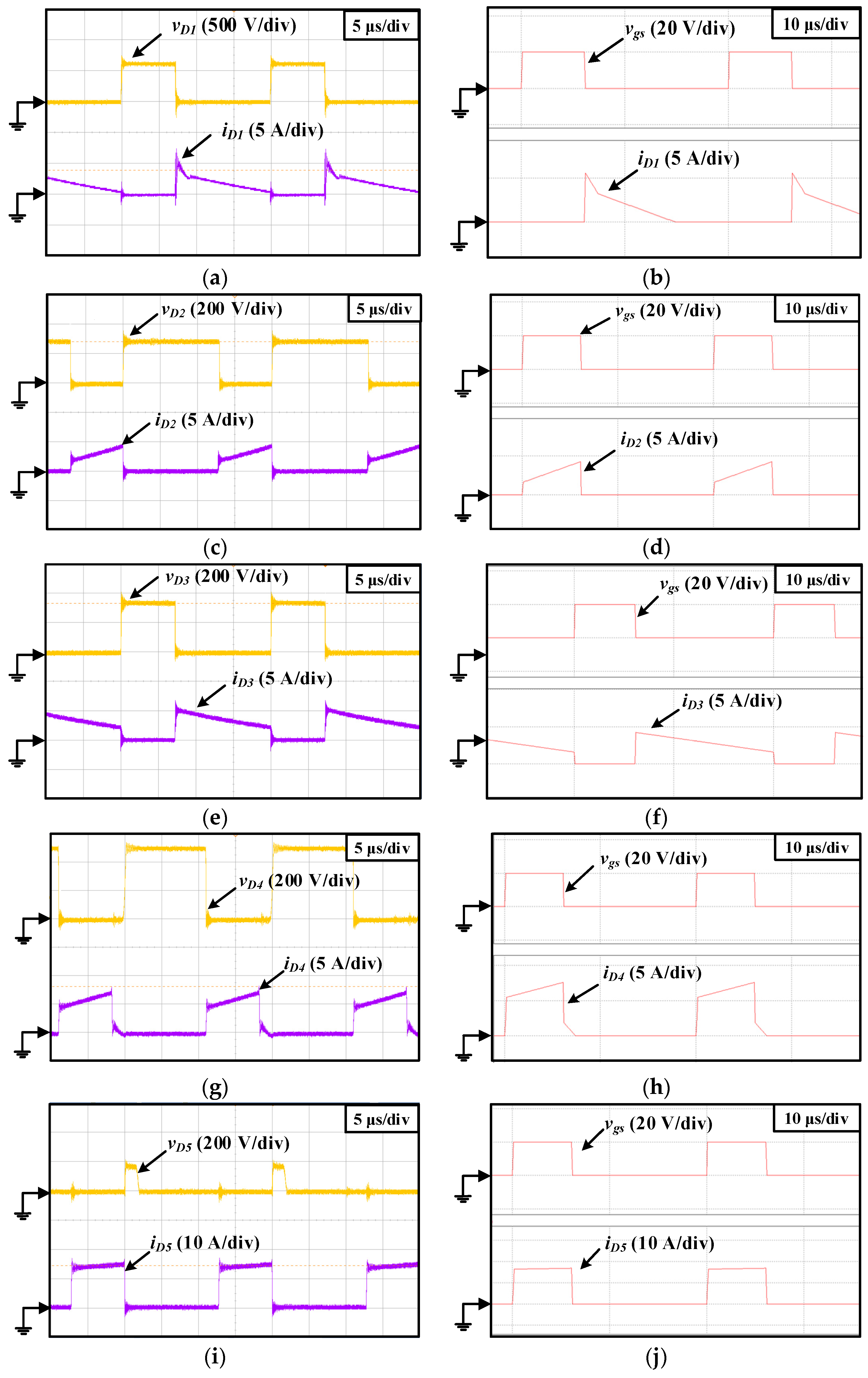
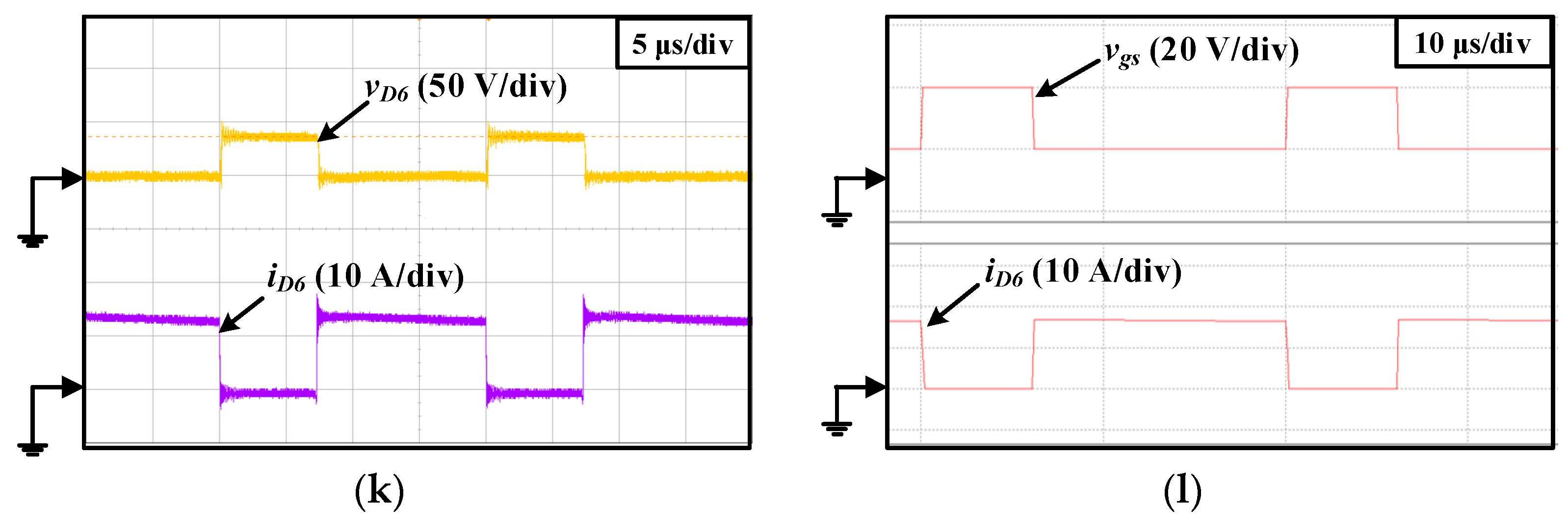
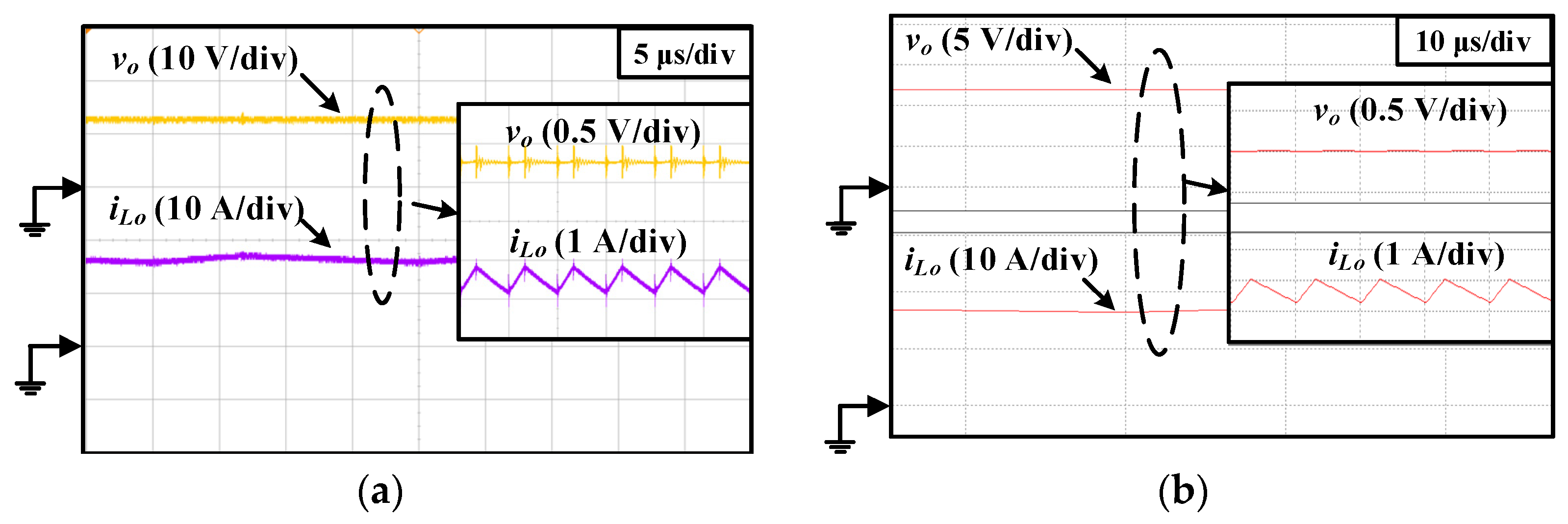
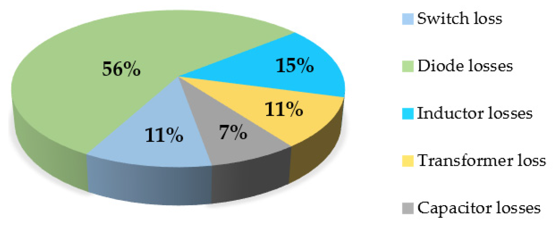
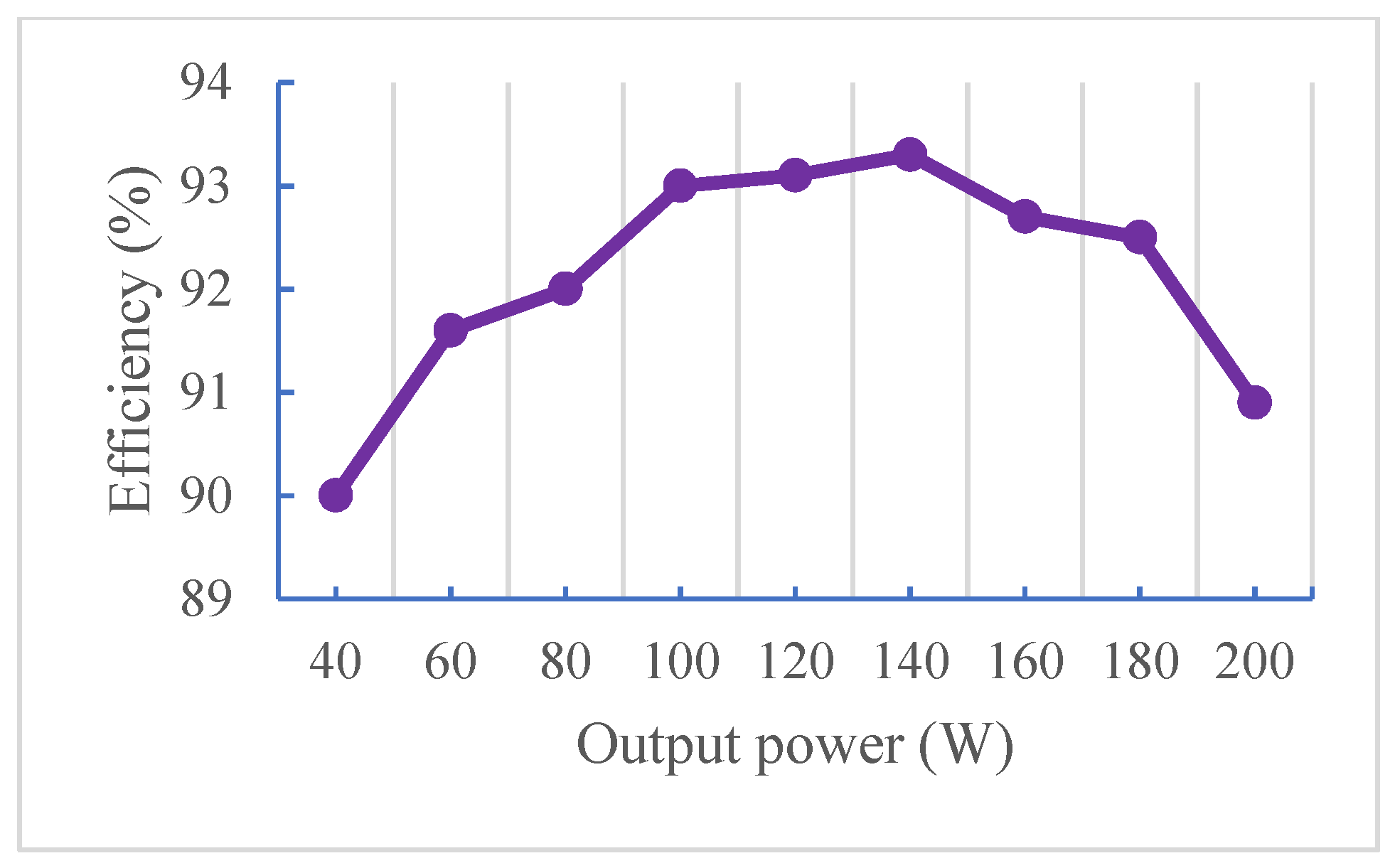
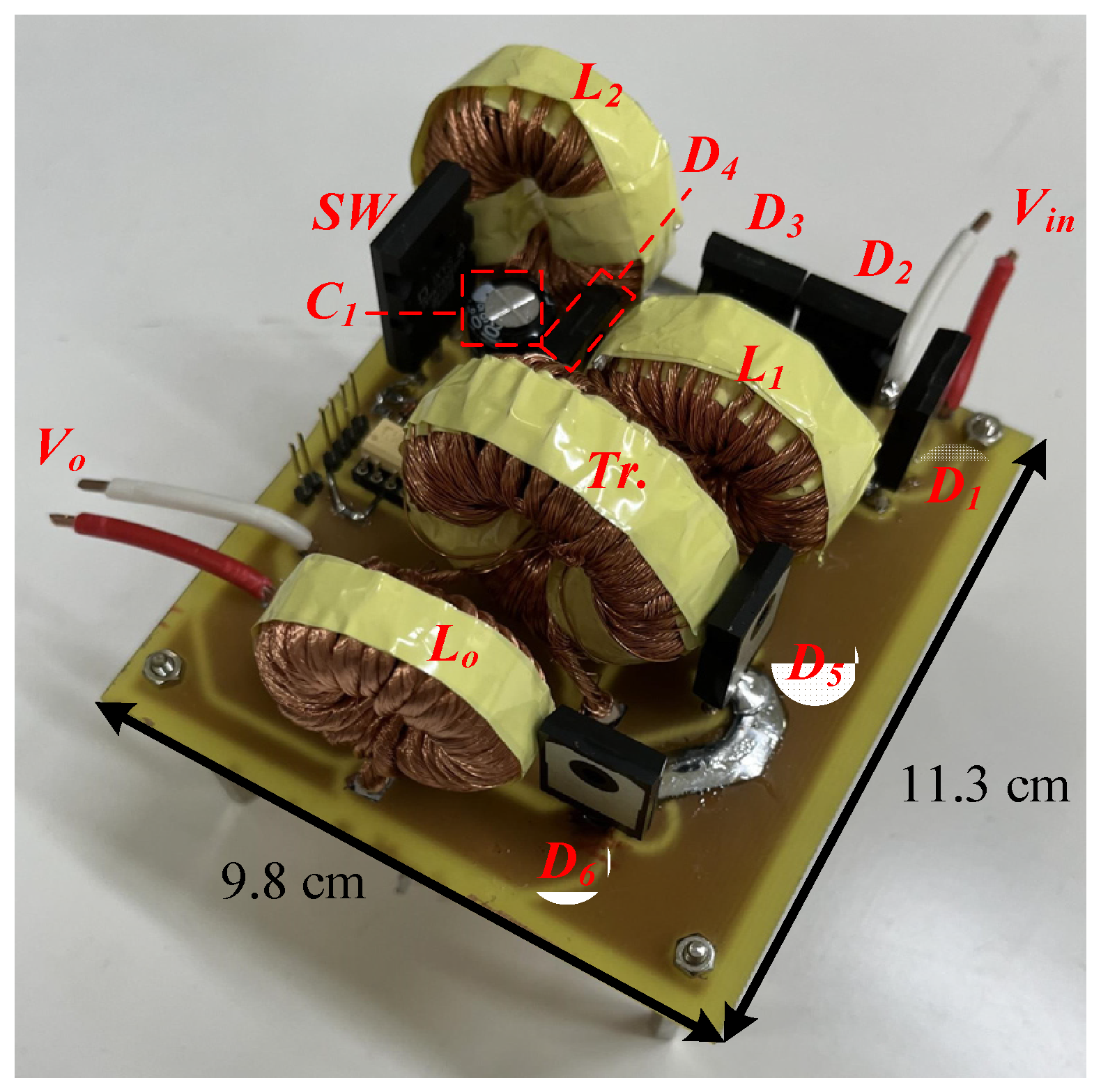
4. Experimental Results
5. Conclusions
Author Contributions
Funding
Conflicts of Interest
References
- Veerachary, M. Two-Switch Semiquadratic Buck Converter. IEEE Trans. Ind. Electron. 2017, 64, 1185–1194. [Google Scholar] [CrossRef]
- Hajiheidari, M.; Farzanehfard, H.; Esteki, M. Asymmetric ZVS Buck Converters with High-Step-Down Conversion Ratio. IEEE Trans. Ind. Electron. 2021, 68, 7957–7964. [Google Scholar] [CrossRef]
- Esteki, M.; Poorali, B.; Adib, E.; Farzanehfard, H. Interleaved Buck Converter with Continuous Input Current, Extremely Low Output Current Ripple, Low Switching Losses, and Improved Step-Down Conversion Ratio. IEEE Trans. Ind. Electron. 2015, 62, 4769–4776. [Google Scholar] [CrossRef]
- Tsai, C.-T.; Shen, C.-L. A High Step-Down Interleaved Buck Converter with Active-Clamp Circuits for Wind Turbines. Energies 2012, 5, 5150–5170. [Google Scholar] [CrossRef] [Green Version]
- Choi, S.; Lee, J.; Lee, J. High-Efficiency Portable Welding Machine Based on Full-Bridge Converter with ISOP-Connected Single Transformer and Active Snubber. IEEE Trans. Ind. Electron. 2016, 63, 4868–4877. [Google Scholar]
- Pei, X.; Nie, S.; Kang, Y. Switch Short-Circuit Fault Diagnosis and Remedial Strategy for Full-Bridge DC–DC Converters. IEEE Trans. Power Electron. 2015, 30, 996–1004. [Google Scholar] [CrossRef]
- Kim, S.; Cha, H.; Ahmed, H.F.; Choi, B.; Kim, H. Isolated Double Step-Down DC–DC Converter with Improved ZVS Range and No Transformer Saturation Problem. IEEE Trans. Power Electron. 2017, 32, 1792–1804. [Google Scholar] [CrossRef]
- Lu, Y.; Wu, K.; Xing, Y. A Family of Isolated Buck-Boost Converters Based on Semiactive Rectifiers for High-Output Voltage Applications. IEEE Trans. Power Electron. 2016, 31, 6327–6340. [Google Scholar] [CrossRef]
- Lee, S.-S.; Yang, Y.; Siwakoti, Y.P.; Barzegarkhoo, R. Improved Cascaded H-Bridge Multilevel Inverters with Voltage-Boosting Capability. Electronics 2021, 10, 2801. [Google Scholar] [CrossRef]
- Liu, Q.; Qian, Q.; Ren, B.; Xu, S.; Yang, L. A Two-Stage Buck–Boost Integrated LLC Converter with Extended ZVS Range and Reduced Conduction Loss for High-Frequency and High-Efficiency Applications. IEEE J. Emerg. Sel. Top. Power Electron. 2021, 9, 727–743. [Google Scholar] [CrossRef]
- Wu, H.; Wan, C.; Sun, K.; Xing, Y. A High Step-Down Multiple Output Converter with Wide Input Voltage Range Based on Quasi Two-Stage Architecture and Dual-Output LLC Resonant Converter. IEEE Trans. Power Electron. 2015, 30, 1793–1796. [Google Scholar] [CrossRef]
- Rueschenbaum, T.; Rehlaender, P.; Ha, P.; Grote, T.; Schafmeister, F.; Boecker, J. Two-Stage Automotive DC-DC Converter Design with Wide Voltage-Transfer Range Utilizing Asymmetric LLC Operation. In Proceedings of the PCIM Europe Digital Days 2020; International Exhibition and Conference for Power Electronics, Intelligent Motion, Renewable Energy and Energy Management, Nuremberg, Germany, 7–8 July 2020; pp. 1–7. [Google Scholar]
- Eckstein, R.H.; Lazzarin, T.B.; Waltrich, G. Two-Stage SEPIC-Buck Topology for Neighborhood Electric Vehicle Charger. In Proceedings of the 2019 IEEE 15th Brazilian Power Electronics Conference and 5th IEEE Southern Power Electronics Conference (COBEP/SPEC), Santos, Brazil, 1–4 December 2019; pp. 1–4. [Google Scholar]
- Alonso, J.M.; Vina, J.; Vaquero, D.G.; Martinez, G.; Osorio, R. Analysis and Design of the Integrated Double Buck–Boost Converter as a High-Power-Factor Driver for Power-LED Lamps. IEEE Trans. Ind. Electron. 2012, 59, 1689–1697. [Google Scholar] [CrossRef]
- Abdelmessih, G.Z.; Alonso, J.M.; Costa, M.A.D.; Chen, Y.-J.; Tsai, W.-T. Fully Integrated Buck and Boost Converter as a High Efficiency, High-Power-Density Off-Line LED Driver. IEEE Trans. Ind. Applicat. 2020, 35, 12238–12251. [Google Scholar] [CrossRef]
- Cosetin, M.R.; Bitencourt, E.A.; Bolzan, T.E.; Silva, M.F.; Alonso, J.M.; do Prado, R.N. Comparison of single stage SEPIC and integrated SEPIC-Buck converter as off-line LED drivers. In Proceedings of the 2013 Brazilian Power Electronics Conference, Gramado, Brazil, 27–31 October 2013; pp. 1134–1139. [Google Scholar]
- Cosetin, M.R.; Bitencourt, E.A.; Bolzan, T.E.; da Silva, M.F.; Alonso, J.M.; do Prado, R.N. Comparison of integrated SEPIC-Buck and SEPIC-Ćuk converters as off-line dimmable LED drivers with reduced storage capacitor. In Proceedings of the 2014 16th European Conference on Power Electronics and Applications, Lappeenranta, Finland, 26–28 August 2014; pp. 1–10. [Google Scholar]
- Almeida, P.S.; Soares, G.M.; Pinto, D.P.; Braga, A.C. Integrated SEPIC Buck-Boost Converter as an Off-line LED Driver without Electrolytic Capacitors. In Proceedings of the IECON 2012-38th Annual Conference on IEEE Industrial Electronics Society, Montreal, QC, Canada, 25–28 October 2012; pp. 4551–4556. [Google Scholar]
- Lee, S.; Do, H. A Single-Switch AC–DC LED Driver Based on a Boost-Flyback PFC Converter with Lossless Snubber. IEEE Trans. Power. Electron. 2017, 32, 1375–1384. [Google Scholar] [CrossRef]
- Zhang, S.; Wang, Y.; Liu, X.; Xu, D. A single-switch integrated-stage LED driver based on Cuk and Class-E converter. In Proceedings of the 2018 International Power Electronics Conference (IPEC-Niigata 2018-ECCE Asia), Niigata, Japan, 20–24 May 2018; pp. 934–938. [Google Scholar]
- Abdelmessih, G.Z.; Alonso, J.M.; Costa, M.A.D. Loss Analysis for Efficiency Improvement of the Integrated Buck–Flyback LED Driver. IEEE Trans. Ind. Applicat. 2018, 54, 6543–6553. [Google Scholar] [CrossRef]
- Yadav, V.K.; Verma, A.K.; Yaragatti, U.R. An Integrated Single Switch AC-DC System for LED Driven by an Unconventional Rectifier. In Proceedings of the 2020 IEEE International Conference on Power Electronics, Drives and Energy Systems (PEDES), Jaipur, India, 16–19 December 2020; pp. 1–6. [Google Scholar]
- Gacio, D.; Alonso, J.M.; Calleja, A.J.; García, J.; Rico-Secades, M. A Universal-Input Single-Stag2e High-Power-Factor Power Supply for HB-LEDs Based on Integrated Buck–Flyback Converter. IEEE Trans. Ind. Electron. 2011, 58, 589–599. [Google Scholar] [CrossRef]
- Poorali, B.; Adib, E. Analysis of the Integrated SEPIC-Flyback Converter as a Single-Stage Single-Switch Power-Factor-Correction LED Driver. IEEE Trans. Ind. Electron. 2016, 63, 3562–3570. [Google Scholar] [CrossRef]
- Tseng, K.-C.; Li, I.-C.; Cheng, C.-A. Integrated Buck and Modified Push−Pull DC−DC Converter with High Step-Down Ratio. IEEE Trans. Ind. Electron. 2020, 67, 235–243. [Google Scholar] [CrossRef]


| Ref. | [3] | [10] | [14] | [25] | Proposed |
|---|---|---|---|---|---|
| Voltage gain | |||||
| MOSFETs | 2 | 6 | 1 | 3 | 1 |
| Diodes | 2 | 0 | 3 | 3 | 6 |
| Capacitors | 3 | 3 | 2 | 3 | 3 |
| Magnetic elements | 3 | 2 | 2 | 3 | 4 |
| Galvanic isolation | No | Yes | No | Yes | Yes |
| Leakage energy recycling | – | Yes | – | Yes | Yes |
| Parameters | Values & Specifications |
|---|---|
| Vin (Input voltage) | 400 V |
| Vo (Output voltage) | 12 V |
| fs (Switch frequency) | 50 kHz |
| Power rating | 200 W |
| Lm1 (Magnetizing inductance) | 366 μH |
| Lk1 (Leakage inductance) | 2.3 μH |
| L1 (Inductor) | 648 μH |
| L2 (Inductor) | 636 μH |
| Lo (Inductor) | 366 μH |
| SW (Power MOSFET) | IXFN60N80P (800 V/53 A), Leiden, Netherlands |
| D1 (Diode) | DSEP29-06A (600 V/30 A), Leiden, Netherlands |
| D2 and D3 (Diode) | BYC8-600 (600 V/8 A), Eindhoven, Netherlands |
| D4 (Diode) | SDP30S120 (1200 V/30 A), Starkville, MS, USA |
| D5 and D6 (Diode) | DSSK 60-02A (200 V/2 × 30 A), Leiden, Netherlands |
| C1 (Electrolytic capacitor) | 47 μF |
| C2 (Electrolytic capacitor) | 4.7 μF |
| Co (Electrolytic capacitor) | 470 μF |
| n (Transformer turns ratio) | 3:1 |
Publisher’s Note: MDPI stays neutral with regard to jurisdictional claims in published maps and institutional affiliations. |
© 2022 by the authors. Licensee MDPI, Basel, Switzerland. This article is an open access article distributed under the terms and conditions of the Creative Commons Attribution (CC BY) license (https://creativecommons.org/licenses/by/4.0/).
Share and Cite
Shen, C.-L.; Chen, L.-Z.; Chuang, T.-Y.; Liang, Y.-S. Cascaded-like High-Step-Down Converter with Single Switch and Leakage Energy Recycling in Single-Stage Structure. Electronics 2022, 11, 352. https://doi.org/10.3390/electronics11030352
Shen C-L, Chen L-Z, Chuang T-Y, Liang Y-S. Cascaded-like High-Step-Down Converter with Single Switch and Leakage Energy Recycling in Single-Stage Structure. Electronics. 2022; 11(3):352. https://doi.org/10.3390/electronics11030352
Chicago/Turabian StyleShen, Chih-Lung, Li-Zhong Chen, Tsung-Yung Chuang, and Yu-Shan Liang. 2022. "Cascaded-like High-Step-Down Converter with Single Switch and Leakage Energy Recycling in Single-Stage Structure" Electronics 11, no. 3: 352. https://doi.org/10.3390/electronics11030352
APA StyleShen, C.-L., Chen, L.-Z., Chuang, T.-Y., & Liang, Y.-S. (2022). Cascaded-like High-Step-Down Converter with Single Switch and Leakage Energy Recycling in Single-Stage Structure. Electronics, 11(3), 352. https://doi.org/10.3390/electronics11030352