Article

Reduced-Cost Optimization-Based Miniaturization of Microwave Passives by Multi-Resolution EM Simulations for Internet of Things and Space-Limited Applications

by
Anna Pietrenko-Dabrowska
1,2,*,
Slawomir Koziel
1,2 and
Ali Ghaffarlouy Raef
2
1
Faculty of Electronics, Telecommunications and Informatics, Gdansk University of Technology, 80-233 Gdansk, Poland
2
Engineering Optimization & Modeling Center, Reykjavik University, 102 Reykjavik, Iceland
*
Author to whom correspondence should be addressed.
Electronics 2022, 11(24), 4094; https://doi.org/10.3390/electronics11244094
Submission received: 4 November 2022 / Revised: 6 December 2022 / Accepted: 7 December 2022 / Published: 8 December 2022
(This article belongs to the Special Issue Advanced RF, Microwave Engineering, and High-Power Microwave Sources)

Abstract

:
Stringent performance specifications along with constraints imposed on physical dimensions make the design of contemporary microwave components a truly onerous task. In recent years, the latter demand has been growing in importance with the innovative application of areas such as the Internet of Things coming into play. The need to employ full-wave electromagnetic (EM) simulations for response evaluation, reliable, yet CPU-heavy, only aggravates the issue. This paper proposes a reduced-cost miniaturization algorithm that employs a trust-region search procedure and multi-resolution EM simulations. In our approach, the resolution of the EM model is adjusted throughout the optimization process based on its convergence status starting from the lowest admissible fidelity. As the algorithm converges, the resolution is increased up to the high-fidelity one, used at the final phase to ensure reliability. Four microwave components have been utilized as verification structures: an impedance matching transformer and three branch-line couplers. Significant savings in terms of the number of EM analyses required to conclude the size reduction process of 41, 42, 38 and 50 percent have been obtained (in comparison to a single-fidelity procedure). The footprint area of the designs optimized using the proposed approach are equal to 32, 205, 410 and 132 mm2, in comparison to 52, 275, 525 and 213 mm2 of the initial (and already compact) design.

1. Introduction

Nowadays, the design of microwave components has become an intricate process that has to satisfy stringent performance requirements, but must also enable the implementation of additional functionalities. Performance specifications pertinent to electrical characteristics of the circuit are typically related to operating frequency and/or frequencies (in the case of multi-band structures), bandwidth, power split ratio, insertion loss levels, allocation of transmission zeros, etc. [1,2,3]. Additional functionalities may include multi-band operation [4,5], tunability [6] or harmonic suppression [7]. Meeting these requirements can be even more challenging due to growing demands for compact size [8,9], which is imperative for emerging applications (e.g., 5G communications [10], Internet of Things (IoT) [11], energy harvesting [12] or sensors [13]). Various methods for miniaturization of microwave components have evolved, including topological modifications, such as transmission line folding [14], employment of compact microstrip resonant cells using the slow-wave phenomenon [15], defected ground structures [16] and high-permittivity substrates [17]. Consequently, compact microwave structures usually feature intricate geometries characterized by large numbers of geometry parameters, simultaneous adjustment of which is indispensable to ascertain the component′s best achievable performance. This, in turn, is of paramount importance, especially for cutting-edge technologies (5G/6G, Internet of Things).
In practice, the tuning process must be executed with the use of full-wave electromagnetic (EM) simulation tools. The employment of EM analysis for the design of compact components is necessary to represent EM cross-coupling effects in tightly packed layouts of miniaturized circuits [18], the effects of environmental components (e.g., connectors) [19], or simply because equivalent network models are grossly inaccurate in characterizing topologically involved structures. On the other hand, rigorous numerical optimization using EM simulations tends to be CPU-heavy. Nevertheless, it is the only approach allowing for the efficient handling of a number of performance figures (e.g., return loss, bandwidth or operating frequency/frequencies), and, at the same time, ensuring control over the physical size of the circuit under study. As the design objectives typically stay in conflict, in practice, the obtained designs constitute trade-offs between the considered performance figures. From a numerical perspective, miniaturization tasks are constrained problems with the constraints being expensive to evaluate. Handling such optimization tasks is numerically demanding, as designs featuring minimum size normally reside at the feasible region boundary. The aforementioned factors make simulation-based miniaturization of microwave components challenging.
The high cost of EM-driven optimization of microwave components, including size-reduction-oriented tasks, is troublesome both in the case of local [20,21,22] and global search [23], especially when using population-based metaheuristics [24,25,26]. Among the techniques designed for streamlining local gradient-based search algorithms, adjoint sensitivities [27,28] and sparse sensitivity updates [29,30,31] may be listed. A completely different strategy is fostered by surrogate-assisted schemes. The surrogate (or a metamodel) is a faster, yet accurate representation of the component under design. There are two kinds of surrogates: physics-based [32] and data-driven [33]. The former involves a low-fidelity representation of the system, e.g., an equivalent circuit. The low-fidelity model is corrected to improve its misalignment with the high-fidelity (EM) model. Representative techniques of this class are space mapping [34], feature-based optimization [35,36] or adaptive response scaling [37]. The second group of surrogates is more generic, as their construction does not require any problem-specific knowledge. The popularity of data-driven models comes from an easy access and versatility (mainly via third-party Matlab toolboxes of many kinds, e.g., SUMO [38], DACE [39], UQlab [40]). Multiple modelling techniques are available, including kriging [41], radial basis functions (RBF) [42], Gaussian process regression [43], support vector regression [44] or neural networks [45,46,47,48]. Still, their applicability is limited by the curse of dimensionality. Setting up reliable surrogates for contemporary microwave devices of intricate topologies and featuring a large number of variables is hardly possible, particularly if the model has to cover broad ranges of operating and geometry parameters (which is imperative from the standpoint of design usability of the model).
This paper proposes an efficient and reliable algorithm for simulation-driven miniaturization of compact microwave components. Our methodology employs multi-fidelity EM simulations selected over a specified range of allowable resolutions: from the minimal (still ensuring satisfactory accuracy) to the high-fidelity model [49]. In addition, the formulation of the design task permits an efficient treatment of design constraints while directly handling size reduction of the structure under design. The entire procedure is embedded into a trust-region gradient-based framework. During the optimization process, the model discretization level is set contingent upon the algorithm convergence status. Adopting the aforementioned mechanisms permits sizeable computational savings without degrading the process reliability. The proposed technique has been employed to miniaturize four compact microwave components: a three-section impedance matching transformer, as well as three branch-line couplers, and is compared to single-fidelity trust-region gradient-based algorithm. The computational cost has been reduced by nearly 50 percent.
The proposed approach enables a rapid rendition of minimum-size microwave components. By means of simultaneous adjustment of all geometry parameters, it allows for additional miniaturization beyond what is possible by pure topology selection of the circuit. Short running time and generality of the presented algorithm make it useful for yielding top-quality structures and to reduce circuit development time, both being of paramount importance for academic research and even more for industry, particularly, in the context of rapidly growing areas including, e.g., the Internet of Things.
The novelty and the technical contributions of the work under review include: (i) development of an algorithm for direct optimization-based miniaturization of microwave components with multi-fidelity EM simulations, (ii) implementation of the size reduction algorithm integrating local gradient-based search with automated adjustment of the model discretization level and (iii) demonstrating a significant speedup of the search process with only a minor increase in the device footprint area with respect to the reference procedure.

2. Miniaturization of Microwave Passives by Multi-Fidelity Simulations

This section describes the proposed miniaturization procedure with multi-resolution EM simulations. The section begins with a formulation of optimization-based miniaturization of microwave passives (Section 2.1). Section 2.2 recalls the standard trust-region algorithm employed in this work as a search engine. The delineation of the multi-fidelity model adjustment scheme and the entire miniaturization framework in Section 2.3 and Section 2.4, respectively, concludes this part of the manuscript.

2.1. Problem Formulation

Nowadays, the design of compact microwave components is more often than not performed through rigorous numerical optimization. Circuit miniaturization is no exception here. In this work, the size reduction task is tackled by solving
x * = arg min x U ( x ) ,
which may also be subject to the inequality constraints gk(x) ≤ 0, k = 1, …, ng, as well as equality constraints hk(x) = 0, k = 1, …, nh. In (1), U is the scalar objective function quantifying the design quality, and x denotes the vector of design variables. For size reduction, U(x) = A(x), with A being the circuit size. Here, we adopt a penalty approach [50], in which the constraints are dealt with in an implicit manner. Thus, the reformulated objective function UP is employed, which accounts for the primary objective (here, the component′s footprint) and other requirements. We have
x * = arg min x U P ( x ) ,
where the function UP is defined as follows
U P ( x ) = U ( x ) + k = 1 n g + n h β k c k ( x )
with ck(x), k = 1, …, ng + nh, representing the penalty functions that quantify constraint violations, whereas βk denotes the penalty coefficients. In (3), the primary objective (size reduction) is supplemented by the contributions proportional to suitably quantified constraint violations. The coefficients βk are typically set up based on designer’s experience on a case-to-case basis.

2.2. Search Engine: Trust-Region Local Search

This section recalls the standard trust-region (TR) algorithm [51], which is exploited here as a search engine. The TR algorithm iteratively yields a series of approximations x(i), i = 0, 1, …, to x* (i.e., the optimal solution), where x(0) denotes the initial design. Each consecutive vector x(i) is established by solving
x ( i + 1 ) = arg min x ; d ( i ) x x ( i ) d ( i ) U L ( i ) ( x ) ,
where UL(i) is defined as UP, but with linear model L(i) of the circuit response R(x). Our principal objective is to reduce the circuit size A(x), which can be evaluated analytically based on the parameter vector x. Thus, there is no need to use the linear model to assess it. Still, when calculating the constraints, the linear expansion model L(i) = R(x(i)) + JR(x(i))·(xx(i)) needs to be employed.

2.3. Model Fidelity Arrangement

Our algorithm exploits multi-fidelity model simulations to expedite miniaturization of microwave passives. Although variable-fidelity frameworks have been employed in antenna [52] and microwave design [53], they typically utilize two levels of resolution: low- and high-fidelity models. Here, we follow the concept introduced in [49], where a continuous range of resolution levels is exploited, delimited by two boundary levels: the lowest one that is still practically useful and the one corresponding to the high-fidelity model. The actual selection of the two levels is of paramount importance. The lowest resolution rmin has to ensure adequate accuracy of the associated model while offering sufficient computational savings, whereas the highest resolution rmax needs to provide an accurate representation of the system outputs.
The model fidelity arrangement utilized in this work is based on the following suppositions: (i) the procedure is initiated with rmin (for the sake of computational savings); (ii) in the consecutive iterations, the resolution r is increased step-by-step, contingent upon the convergence status of the optimization procedure; and (iii) close to the termination, rmax is enforced (for the sake of reliability).
The following factor assessing the convergence status is defined as
Q ( i ) ( ε x , ε U ) = max ε x | | x ( i + 1 ) x ( i ) | | , ε U | U P ( x ( i + 1 ) ) U P ( x ( i ) ) |
with εx and εU referring to the user-defined termination thresholds. The optimization procedure has reached convergence if the following holds: ||x(i+1)x(i)|| < εx (the design shift between iterations is small) OR ||d(i)|| < εx (the TR size is sufficiently reduced) OR |UP(x(i+1)) − UP(x(i))| < εU (the change of the merit function value between iterations is minor). The factor Q(i) serves for adjusting the value of the model discretization level r(i+1) for the next algorithm iteration according to
r ( i + 1 ) = r min if Q ( i ) ( ε x , ε U ) M max r ( i ) , r min + r max r min Q ( i ) ( ε x , ε U ) M 1 α
In (6), M governs the onset of the model resolution increase (with respect to the algorithm convergence) and α is a shape parameter. By setting M = 10–2 and α = 3 (as in Section 3), the model resolution starts to increase (relatively rapidly) two decades prior to convergence, which is beneficiary for computational efficiency.
Nevertheless, Formula (6) does not guarantee that the final iterations are performed using the highest model resolution (which is mandatory from the standpoint of reliability). Thus, a safeguard mechanism must be implemented, which works as follows: in the final iteration, if r(i) < rmax, then the termination condition is ignored. Consequently, for the next (supplemental) iteration, the model resolution is set to r(i+1) = rmax and the TR size is set as d(i+1) = Md d(i) εx/||d(i)||, where the multiplier Md determines the increase in the TR size to ensure sufficient space for design tuning after shifting to the maximum resolution. Here, we adopt Md = 10.
To achieve additional speedup, response gradients are evaluated at a resolution rFD = max{rmin, λr(i)}, which is lower than the current resolution used for simulation of the model outputs. The factor λ assumes positive values below 1; in our work, we set λ = 2/3.
Given a typical time evaluation ratio between the highest- and lowest-fidelity model to be about three, one can estimate the expected reduction of the computational cost of the optimization process at a level of about fifty percent. This is because most of the operations will be performed using lower-fidelity EM simulations, yet the last few iterations executed using the high-fidelity model will contribute to perhaps half of the total cost. That half, as being spanned over 1/5 to 1/4 of the overall iteration span, allows us to estimate the total cost as being half of that corresponding to the high-fidelity only version of the algorithm. This is, clearly, a very rough estimate, which highly depends on several factors, including the said time evaluation ratio.

2.4. Miniaturization Framework

The operational flow of the optimization-based multi-fidelity miniaturization algorithm discussed here is presented in Figure 1, whereas its pseudocode is presented in Algorithm 1. The algorithm exploits two main components: the trust region algorithm of Section 2.2 and the multi-fidelity model arrangement formulated in Section 2.3. The algorithm control parameters are gathered in Table 1.
Algorithm 1: Operation of the proposed multi-fidelity size reduction algorithm.
1. Set the iteration counter i = 0, and r(i) = rmin;
2. Evaluate component response R(x(i)) at the discretization level r(i);
3. Evaluate component sensitivities JR(x(i)) at the discretization level rFD;
4. Construct a linear model L ( i ) ( x ) = R ( x ( i ) ) + J R ( x ( i ) ) ( x x ( i ) ) ;
5. Obtain the design x(i+1) by solving (4);
6. Evaluate component response R(x(i+1)) at the discretization level r(i);
7. Update trust-region size vector d(i);
8. If UP(x(i+1)) < UP(x(i)),
      compute r(i+1) using (6);
      Set i = i + 1;
end
9. If ||x(i+1)x(i)|| < εx OR ||d(i)|| < εx OR | UP(x(i+1)) – UP(x(i))| < εU
if r(i) < rmax
      Set r(i) = rmax and modify d(i); go to 3;
else
      Go to 10;
end
else
      Go to 3;
end
10. END.
We employed CST Microwave Studio for evaluation of the computational models of the considered devices. Hence, the model discretization is parametrized by LPW (lines per wavelength), utilized in CST to govern the mesh density. The boundary resolution levels rmin and rmax were decided upon through the grid convergence studies, as presented in Section 3. The maximum resolution level rmax is the resolution increasing above, which leads to no meaningful changes of the component characteristics, whereas rmin is assessed as the lowest resolution for which the evaluated responses outputs are still adequately rendered.

3. Results

This section provides the results obtained using the introduced size-reduction algorithm with multi-resolution EM-simulations for four microwave passive devices: a three-section impedance transformer and three branch-line couplers. The design goals for the transformer are footprint minimization and in-band matching enhancement. For the couplers, we have three design objectives: (i) footprint minimization, (ii) minimization of matching and isolation and (iii) enforcement of an assumed power split (equal in the case of two couplers, and unequal for the third one).
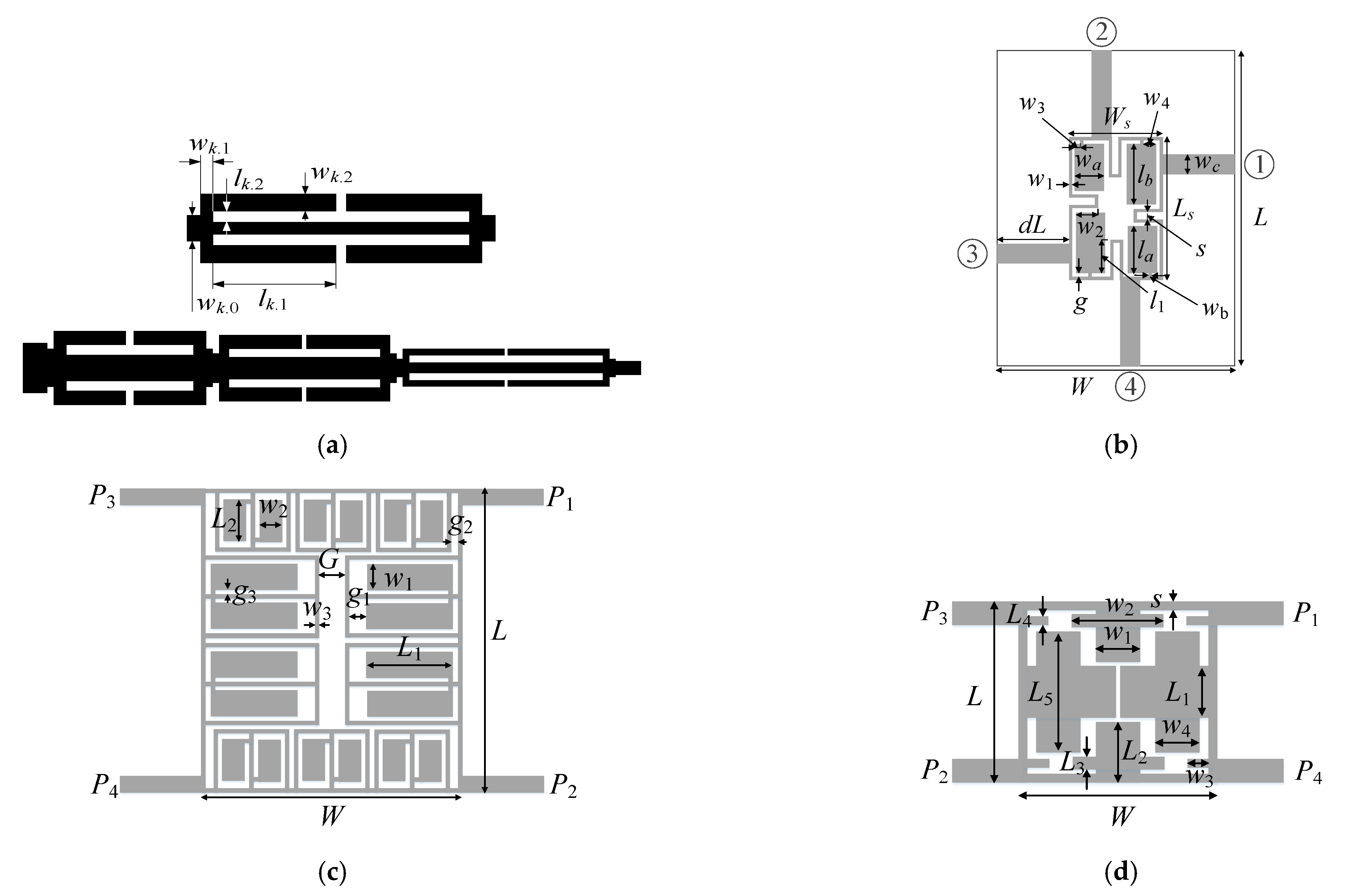
Figure 2 shows the geometries of four microwave devices utilized here as verification case studies: a three-section impedance transformer comprising three compact microstrip resonant cell (CMRC) sections (Circuit I), a compact branch-line coupler (Circuit II), a branch-line coupler with microstrip cells (Circuit III) and a branch-line coupler with unequal power division (Circuit IV). Table 2 gathers all the necessary information pertaining to all circuits: the geometry parameters (the relative and unit-less parameters are indicated by the subscript r; the remaining ones are absolute and expressed in mm), the substrate they are implemented on, the design goals, the objective function formulation and variable-fidelity simulations setup.
Table 2 also provides the values of the penalty coefficients (cf. (3)), which determine the contribution of the penalty terms to make them commensurable to that of the main objective (here, footprint miniaturization). The said values have been set up for each verification case individually. The computational models are evaluated using the time-domain solver of CST Microwave Studio and I dependence of the simulation time on the parameter LPW is presented in Figure 3. The proposed framework utilizes the default control parameter values provided in Table 1.
Our procedure is benchmarked against the conventional single-fidelity trust-region procedure with numerical derivatives to verify the acceleration rate achieved due to the involvement of variable-resolution models, as well as to investigate possible design quality degradation. The following performance factors are taken into account: the footprint of the circuit at the optimal design, along with the computational cost of rendering it. As far as multi-fidelity algorithm is concerned, the actual model simulation times for each resolution level are assessed as the equivalent number of simulations of the highest resolution rmax.
Table 3 gathers the optimization results obtained for all circuits using the introduced algorithm and the conventional TR algorithm utilized here as a reference routine. The results comprise the expenditures of the optimization procedure expressed as the equivalent number of high-fidelity circuit analyses (evaluated using the time evaluation curves of Figure 3), along with the savings with regard to the TR search. Moreover, Table 3 provides the footprint of all the verification structures. Figure 4, Figure 5, Figure 6 and Figure 7 present the responses of the respective circuits at the initial and optimized designs, as well the evolution of circuit size throughout the algorithm runs.
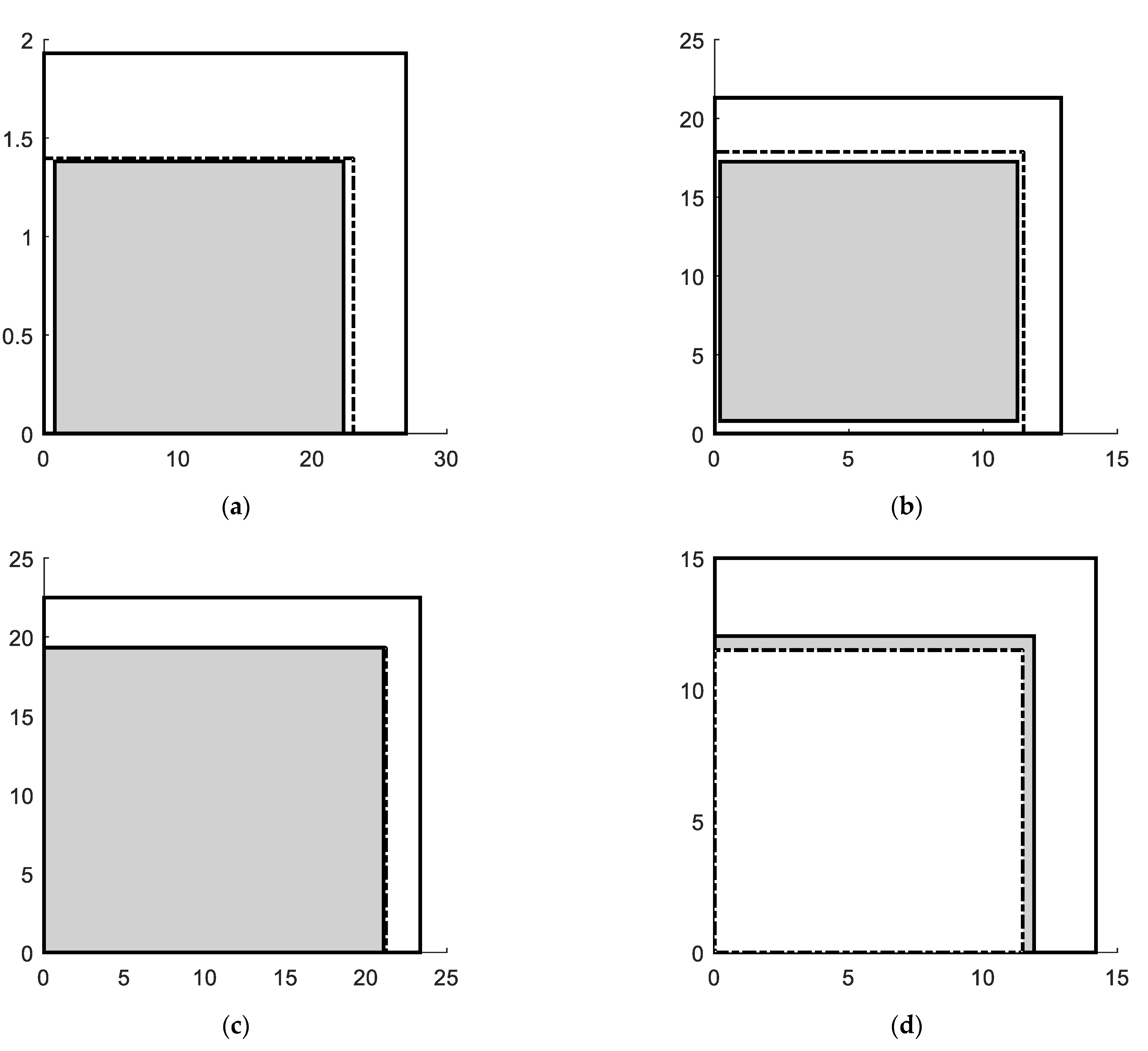
Comparison of the proposed miniaturization framework based on multi-fidelity simulations with the conventional single-fidelity trust-region gradient based algorithm allows us to draw the following conclusions: our approach allows for achieving significant miniaturization rates equal to around 38, 25, 22 and 38 percent (31 percent on average) for Circuits I through IV, respectively, with respect to the initial (and already compact) structure size, whereas for the benchmark TR algorithm, we have 42, 34, 22 and 33 (33 on average). Thus, the size of the optimized designs with respect to the area of the initial design for the proposed and benchmark procedure, are comparable. In the case of Circuits I through III, the footprints of the optimal designs are only 7, 11 and 1 percent larger than those rendered by the conventional TR algorithm, whereas the area of the Circuit IV is eight percent smaller. For the sake of comparison, the footprints of the initial and optimized designs are shown in Figure 8.
The said miniaturization rates are accompanied by a considerable computational savings of around 43 percent on the average (see Table 3). This means that incorporating multi-resolution EM simulations allows for accelerating the optimization-based miniaturization process almost twice on the average at the cost of slightly degraded miniaturization rates. Measuring in absolute numbers, the average CPU cost corresponds to around sixty high-fidelity EM simulations, meaning that the typical execution time only takes around three hours.

4. Conclusions

The paper proposed a novel framework for optimization-based EM-driven size reduction of microwave circuits. Our approach exploits multi-fidelity EM simulations, which are embedded into the core gradient-based optimization algorithm. The management of the circuit discretization level during the optimization run is contingent upon its convergence status: from the lowest one, used when the procedure is launched, to the highest resolution utilized near reaching optimum. Consequently, a significant speedup of the miniaturization procedure been obtained in comparison to a single-fidelity version with similar miniaturization rates. The performance of the proposed size-reduction framework has been comprehensively verified using four microwave devices: an impedance transformer and three branch-line couplers, all optimized for a minimum size. Additionally, minimization of matching within the frequency band of interest has been carried out in the case of the transformer, whereas the couplers have been optimized for best matching and isolation. The savings, with respect to a single-fidelity procedure, have been equal to 41, 42, 38 and 50 percent, across the benchmark set. In the proposed approach, optimal designs feature truly compact sizes: 32, 205, 410 and 132 mm2 (in comparison to 52, 275, 525 and 213 mm2 of the initial design). It should be emphasized that size reduction of microwave components has become critical for a number of applications, including the Internet of Things. The proposed approach offers a design enhancement solution that is fast to execute, fully automated and complements traditional design methods (here, the initial development of compact circuit topology). These features make it an attractive tool, especially in an industrial context, but also in academic research.

Author Contributions

Conceptualization, A.P.-D. and S.K.; methodology, A.P.-D. and S.K.; software, A.P.-D. and A.G.R.; validation, A.P.-D. and S.K.; formal analysis, A.P.-D. and S.K.; investigation, A.P.-D.; resources, S.K.; data curation, A.P.-D. and A.G.R.; writing—original draft preparation, A.P.-D. and S.K.; writing—review and editing, A.P.-D. and S.K.; visualization, A.P.-D. and A.G.R.; supervision, S.K.; project administration, S.K.; funding acquisition, S.K. All authors have read and agreed to the published version of the manuscript.

Funding

The research leading to these results has received funding from the Norway Grants 2014-2021 via the National Centre for Research and Development, grant NOR/POLNOR/HAPADS/0049/2019-00. This work was also supported in part by the Icelandic Centre for Research (RANNIS) Grant 217771.

Institutional Review Board Statement

Not applicable.

Informed Consent Statement

Not applicable.

Data Availability Statement

Data sharing not applicable.

Acknowledgments

The authors thank Dassault Systemes, France, for making the CST Microwave Studio available.

Conflicts of Interest

The authors declare no conflict of interest. The funders had no role in the design of the study; in the collection, analyses or interpretation of data; in the writing of the manuscript, or in the decision to publish the results.

References

  1. Cai, L.; Cheng, K.M. A novel design of dual-band rat-race coupler with reconfigurable power-dividing ratio. IEEE Microwave Wireless Comp. Lett. 2018, 28, 16–18. [Google Scholar] [CrossRef]
  2. Li, Q.; Chen, X.; Chi, P.; Yang, T. Tunable bandstop filter using distributed coupling microstrip resonators with capacitive terminal. IEEE Microw. Wirel. Comp. Lett. 2020, 30, 35–38. [Google Scholar] [CrossRef]
  3. Chen, S.; Yu, Y.; Tang, M. Dual-band Gysel power divider with different power dividing ratios. IEEE Microw. Wirel. Comp. Lett. 2019, 29, 462–464. [Google Scholar] [CrossRef]
  4. Chi, P.; Chen, Y.; Yang, T. Single-layer dual-band balanced substrate- integrated waveguide filtering power divider for 5G millimeter-wave applications. IEEE Microw. Wirel. Comp. Lett. 2020, 30, 585–588. [Google Scholar] [CrossRef]
  5. Seddiki, M.L.; Nedil, M.; Ghanem, F. A novel wide, dual-and triple-band frequency reconfigurable butler matrix based on transmission line resonators. IEEE Access 2019, 7, 1840–1847. [Google Scholar] [CrossRef]
  6. Ebrahimi, A.; Baum, T.; Scott, J.; Ghorbani, K. Continuously tunable dual-mode bandstop filter. IEEE Microw. Wirel. Comp. Lett. 2018, 28, 419–421. [Google Scholar] [CrossRef] [Green Version]
  7. Tsai, K.; Yang, H.; Chen, J.; Chen, Y.E. A miniaturized 3 dB branch-line hybrid coupler with harmonics suppression. IEEE Microw. Wirel. Comp. Lett. 2011, 21, 537–539. [Google Scholar] [CrossRef]
  8. Lin, Y.-S.; Liu, Y.-R.; Chan, C.-H. Novel miniature dual-band rat-race coupler with arbitrary power division ratios using differential bridged-T coils. IEEE Trans. Microw. Theory Tech. 2021, 69, 590–602. [Google Scholar] [CrossRef]
  9. Mocanu, I.A. Compact dual band ring coupler using miniaturized metamaterial left-handed impedance inverters. IEEE Access 2021, 9, 86119–86131. [Google Scholar] [CrossRef]
  10. Hussain, R. Shared-aperture slot-based sub-6-GHz and mm-Wave IoT antenna for 5G applications. IEEE IoT J. 2021, 8, 10807–10814. [Google Scholar] [CrossRef]
  11. Hussain, N.; Kim, N. Integrated microwave and mm-Wave MIMO antenna module with 360° pattern diversity for 5G Internet-of-Things. IEEE IoT J. 2022, 9, 24777–24789. [Google Scholar] [CrossRef]
  12. Lorenz, C.H.P.; Hemour, S.; Liu, W.; Badel, A.; Formosa, F.; Wu, K. Hybrid power harvesting for increased power conversion efficiency. IEEE Microw. Wirel. Comp. Lett. 2015, 25, 687–689. [Google Scholar] [CrossRef]
  13. Dinh, D.D.; Lancaster, M.J. Microwave power sensors with integrated filtering function for transfer power standards. IEEE Microw. Wirel. Comp. Lett. 2020, 30, 308–311. [Google Scholar] [CrossRef]
  14. Kosuge, A.; Kadomoto, J.; Kuroda, T. A 6 Gb/s 6 pJ/b 5 mm-distance non-contact interface for modular smartphones using two-fold transmission line coupler and high EMC tolerant pulse transceiver. IEEE J. Solid-State Circ. 2016, 51, 1446–1456. [Google Scholar] [CrossRef]
  15. Shum, K.M.; Mo, T.T.; Xue, Q.; Chan, C.H. A compact bandpass filter with two tuning transmission zeros using a CMRC resonator. IEEE Trans. Microw. Theory Tech. 2015, 53, 895–900. [Google Scholar] [CrossRef]
  16. Han, C.; Tang, D.; Deng, Z.; Qian, H.J.; Luo, X. Filtering power divider with ultrawide stopband and wideband low radiation loss using substrate integrated defected ground structure. IEEE Microw. Wirel. Comp. Lett. 2021, 31, 113–116. [Google Scholar] [CrossRef]
  17. Alqadami, A.S.M.; Nguyen-Trong, N.; Mohammed, B.; Stancombe, A.E.; Heitzmann, M.T.; Abbosh, A. Compact unidirectional conformal antenna based on flexible high-permittivity custom-made substrate for wearable wideband electromagnetic head imaging system. IEEE Trans. Antennas Propag. 2020, 68, 183–194. [Google Scholar] [CrossRef]
  18. Wang, D.-M.; Hu, J.-G.; Wu, J. A fully integrated low-cost HF multi-standard RFID reader SoC and module for IoT applications. IEEE IoT Journal. 2022, 9, 19201–19213. [Google Scholar] [CrossRef]
  19. Kurgan, P.; Koziel, S. Selection of circuit geometry for miniaturized microwave components based on concurrent optimization of performance and layout area. AEÜ–Int. J. Electr. Comm. 2019, 108, 287–294. [Google Scholar] [CrossRef]
  20. Tomasson, J.A.; Koziel, S.; Pietrenko-Dabrowska, A. Quasi-global optimization of antenna structures using principal components and affine subspace-spanned surrogates. IEEE Access 2020, 8, 50078–50084. [Google Scholar] [CrossRef]
  21. Kolda, T.G.; Lewis, R.M.; Torczon, V. Optimization by direct search: New perspectives on some classical and modern methods. SIAM Rev. 2003, 45, 385–482. [Google Scholar] [CrossRef] [Green Version]
  22. Pietrenko-Dabrowska, A.; Koziel, S. Expedited antenna optimization with numerical derivatives and gradient change tracking. Eng. Comput. 2020, 37, 1179–1193. [Google Scholar] [CrossRef]
  23. Liu, B.; Yang, H.; Lancaster, M.J. Global optimization of microwave filters based on a surrogate model-assisted evolutionary algorithm. IEEE Trans. Microw. Theory Techn. 2017, 65, 1976–1985. [Google Scholar] [CrossRef] [Green Version]
  24. Zhao, W.; Liu, E.-X.; Wang, B.; Gao, S.; Png, C.E. Differential evolutionary optimization of an equivalent dipole model for electromagnetic emission analysis. IEEE Trans. Electromagn. Compat. 2018, 60, 1635–1639. [Google Scholar] [CrossRef]
  25. Lalbakhsh, A.; Afzal, M.U.; Esselle, K.P. Multiobjective particle swarm optimization to design a time-delay equalizer metasurface for an electromagnetic band-gap resonator antenna. IEEE Antenna Wirel. Comp. Lett. 2017, 16, 912–915. [Google Scholar] [CrossRef]
  26. Yang, C.; Zhang, J.; Tong, M.S. An FFT-accelerated particle swarm optimization method for solving far-field inverse scattering problems. IEEE Trans. Antennas Propag. 2021, 69, 1078–1093. [Google Scholar] [CrossRef]
  27. Koziel, S.; Ogurtsov, S.; Cheng, Q.S.; Bandler, J.W. Rapid EM-based microwave design optimization exploiting shape-preserving response prediction and adjoint sensitivities. IET Microw. Ant. Prop. 2014, 8, 775–781. [Google Scholar] [CrossRef]
  28. Feng, F.; Na, W.; Liu, W.; Yan, S.; Zhu, L.; Zhang, Q.-J. Parallel gradient-based EM optimization for microwave components using adjoint- sensitivity-based neuro-transfer function surrogate. IEEE Trans. Microw. Theory Tech. 2020, 68, 3606–3620. [Google Scholar] [CrossRef]
  29. Pietrenko-Dabrowska, A.; Koziel, S. Numerically efficient algorithm for compact microwave device optimization with flexible sensitivity updating scheme. Int. J. RF Microw. Comput. Aided Eng. 2019, 29, e21714. [Google Scholar] [CrossRef]
  30. Koziel, S.; Pietrenko-Dabrowska, A. Efficient gradient-based algorithm with numerical derivatives for expedited optimization of multi-parameter miniaturized impedance matching transformers. Radioengineering 2019, 27, 572–578. [Google Scholar] [CrossRef]
  31. Koziel, S.; Pietrenko-Dabrowska, A. Reduced-cost design closure of antennas by means of gradient search with restricted sensitivity updates. Metrol. Meas. Syst. 2019, 26, 595–605. [Google Scholar]
  32. Zhang, W.; Feng, F.; Gongal-Reddy, V.-M.-R.; Zhang, J.; Yan, S.; Ma, J.; Zhang, Q.J. Space mapping approach to electromagnetic centric multiphysics parametric modeling of microwave components. IEEE Trans. Microw. Theory Tech. 2018, 66, 3169–3185. [Google Scholar] [CrossRef]
  33. Cai, J.; King, J.; Yu, C.; Liu, J.; Sun, L. Support vector regression-based behavioral modeling technique for RF power transistors. IEEE Microw. Wirel. Comp. Lett. 2018, 28, 428–430. [Google Scholar] [CrossRef]
  34. Melgarejo, J.C.; Ossorio, J.; Cogollos, S.; Guglielmi, M.; Boria, V.E.; Bandler, J.W. On space mapping techniques for microwave filter tuning. IEEE Trans. Microw. Theory Tech. 2019, 67, 4860–4870. [Google Scholar] [CrossRef]
  35. Koziel, S.; Bandler, J.W. Reliable microwave modeling by means of variable-fidelity response features. IEEE Trans. Microw. Theory Tech. 2015, 63, 4247–4254. [Google Scholar] [CrossRef]
  36. Pietrenko-Dabrowska, A.; Koziel, S. Fast design closure of compact microwave components by means of feature-based metamodels. Electronics 2021, 10, 10. [Google Scholar] [CrossRef]
  37. Koziel, S.; Unnsteinsson, S.D. Expedited design closure of antennas by means of trust-region-based adaptive response scaling. IEEE Antenna Wirel. Comp. Lett. 2018, 17, 1099–1103. [Google Scholar] [CrossRef]
  38. Gorissen, D.; Crombecq, K.; Couckuyt, I.; Dhaene, T.; Demeester, P. A surrogate modeling and adaptive sampling toolbox for computer based design. J. Mach. Learn. Res. 2010, 11, 2051–2055. [Google Scholar]
  39. Lophaven, S.N.; Nielsen, H.B.; Søndergaard, J. DACE: A MATLAB Kriging Toolbox; Tech. Rep. IMMTR-2002-12; Technical University of Denmark: Lyngby, Denmark, 2002. [Google Scholar]
  40. Marelli, S.; Sudret, B. UQLab: A framework for uncertainty quantification in MATLAB. In Vulnerability, Uncertainty, and Risk: Quantification, Mitigation, and Management; ASCE Library: London, UK, 2014; pp. 2554–2563. [Google Scholar]
  41. Hassan, A.S.O.; Etman, A.S.; Soliman, E.A. Optimization of a novel nano antenna with two radiation modes using kriging surrogate models. IEEE Photonics J. 2018, 10, 4800807. [Google Scholar] [CrossRef]
  42. Xiao, L.; Shao, W.; Jin, F.; Wang, B.; Joines, W.T.; Liu, Q.H. Semisupervised radial basis function neural network with an effective sampling strategy. IEEE Trans. Microw. Theory Tech. 2020, 68, 1260–1269. [Google Scholar] [CrossRef]
  43. Jacobs, J.P.; Koziel, S. Two-stage framework for efficient Gaussian process modeling of antenna input characteristics. IEEE Trans. Antennas Propag. 2014, 62, 706–713. [Google Scholar] [CrossRef] [Green Version]
  44. Prado, D.R.; Lopez-Fernandez, J.A.; Arrebola, M.; Goussetis, G. Support vector regression to accelerate design and crosspolar optimization of shaped-beam reflectarray antennas for space applications. IEEE Trans. Antennas Propag. 2019, 67, 1659–1668. [Google Scholar] [CrossRef]
  45. Cui, J.; Feng, F.; Na, W.; Zhang, Q.-J. Bayesian-based automated model generation method for neural network modeling of microwave components. IEEE Microw. Wirel. Comp. Lett. 2023, 31, 1179–1182. [Google Scholar] [CrossRef]
  46. Jin, J.; Feng, F.; Zhang, J.; Yan, S.; Na, W.; Zhang, Q.J. A novel deep neural network topology for parametric modeling of passive microwave components. IEEE Access 2020, 8, 82273–82285. [Google Scholar] [CrossRef]
  47. Zhang, W.; Feng, F.; Jin, J.; Zhang, Q.-J. Parallel multiphysics optimization for microwave devices exploiting neural network surrogate. IEEE Microw. Wirel. Comp. Lett. 2021, 31, 341–344. [Google Scholar] [CrossRef]
  48. Liu, Z.-X.; Shao, W.; Ding, X.; Peng, L.; Jiang, B. Neural network with Fourier series-based transfer functions for filter modeling. IEEE Microw. Wirel. Comp. Lett. 2022, 32, 823–826. [Google Scholar] [CrossRef]
  49. Koziel, S.; Pietrenko-Dabrowska, A.; Plotka, P. Reduced-cost microwave design closure by multi-resolution EM simulations and model management. IEEE Access 2021, 9, 116326–116337. [Google Scholar] [CrossRef]
  50. Nocedal, J.; Wright, S.J. Numerical Optimization, 2nd ed.; Springer: New York, NY, USA, 2001. [Google Scholar]
  51. Conn, A.R.; Gould, N.I.M.; Toint, P.L. Trust Region Methods; MPS-SIAM Series on Optimization; Society for Industrial and Applied Mathematics: Philadelphia, PA, USA, 2000. [Google Scholar]
  52. Koziel, S.; Pietrenko-Dabrowska, A. Variable-fidelity simulation models and sparse gradient updates for cost-efficient optimization of compact antenna input characteristics. Sensors 2019, 19, 1806. [Google Scholar] [CrossRef] [Green Version]
  53. Koziel, S.; Bekasiewicz, A. Fast EM-driven optimization using variable-fidelity EM models and adjoint sensitivities. IEEE Microw. Wirel. Comp. Lett. 2016, 26, 80–82. [Google Scholar] [CrossRef]
  54. Koziel, S.; Pietrenko-Dabrowska, A. Reliable data-driven modeling of high-frequency structures by means of nested kriging with enhanced design of experiment. Eng. Comput. 2019, 36, 2293–2308. [Google Scholar] [CrossRef]
  55. Tseng, C.-H.; Chang, C.-L. A rigorous design methodology for compact planar branch-line and rat-race couplers with asymmetrical T-structures. IEEE Trans. Microw. Theory Tech. 2012, 60, 2085–2092. [Google Scholar] [CrossRef]
  56. Letavin, D.A.; Shabunin, S.N. Miniaturization of a branch-line coupler using microstrip cells. In Proceedings of the 2018 XIV International Scientific-Technical Conference on Actual Problems of Electronics Instrument Engineering (APEIE), Novosibirsk, Russia, 2–6 October 2018; pp. 62–65. [Google Scholar]
  57. Letavin, D.A.; Mitelman, E.; Chechetkin, V.A. Compact microstrip branch-line coupler with unequal power division. In Proceedings of the 2017 11th European Conference on Antennas and Propagation, EUCAP 2017, Paris, France, 19–24 March 2017; pp. 1162–1165. [Google Scholar]
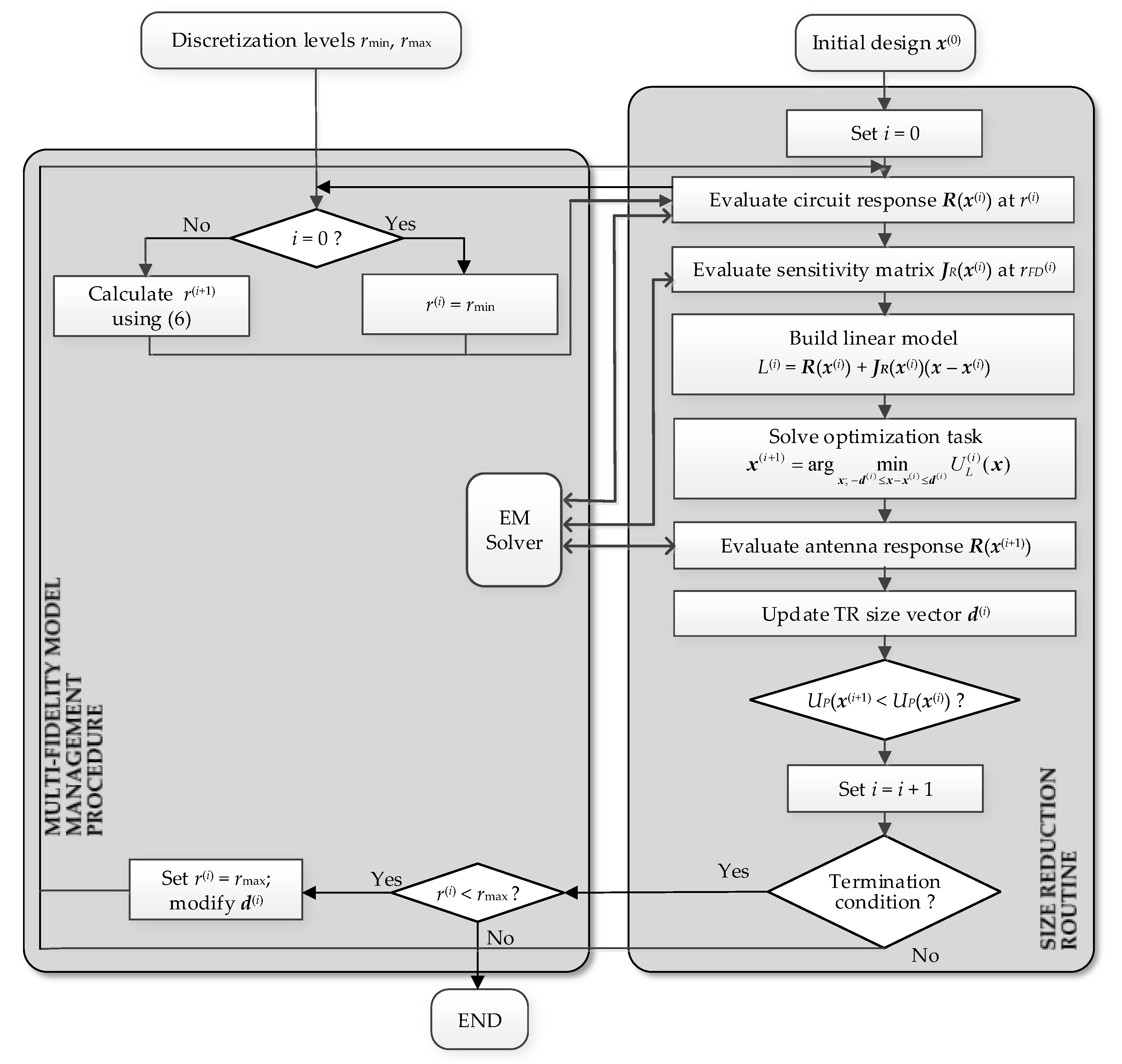
Figure 1. Operational flow of the proposed optimization-based miniaturization framework with multi-resolution EM simulations (one-headed arrows indicate the procedure flow, whereas two-headed arrows show where the procedure accesses the EM solver).
Electronics 11 04094 g001
Figure 2. Verification structures: (a) three-section impedance matching transformer: (top) compact microstrip resonant cell (CMRC), (bottom) geometry of the circuit using CMRCs (Circuit I) [54]; (b) compact branch-line coupler (Circuit II) [55]; the numbers in circles show ports; (c) branch-line coupler with microstrip cells (Circuit III) [56], (d) compact branch-line coupler with unequal power division (Circuit IV) [57].
Electronics 11 04094 g002
Figure 3. The dependence on the simulation time versus model resolution expressed using LPW: (ad) Circuit I through IV, respectively; the low-fidelity model (- - -) and the high-fidelity model (—) are shown using vertical lines.
Electronics 11 04094 g003
Figure 4. Circuit I: (a) responses at the initial (A0 = 52 mm2) (gray) and design optimized using the proposed algorithm (reduced size: Aopt = 31 mm2) (black); the red horizontal line marks the design specifications; (b) evolution of the circuit size throughout the optimization run.
Electronics 11 04094 g004
Figure 5. Circuit II: (a) responses at the initial (A0 = 275 mm2) and design optimized using the proposed algorithm (reduced size: Aopt = 205 mm2), indicated using gray and black, respectively; S-parameters marked as |S11| (—), |S21| (····), |S31| (- - -), |S41| (- .); the vertical line marks the circuit operating frequency; (b) evolution of the circuit size throughout the optimization run.
Electronics 11 04094 g005
Figure 6. Circuit III: (a) responses at the initial (A0 = 525 mm2) and design optimized using the proposed algorithm (reduced size: Aopt = 409 mm2), indicated using gray and black, respectively; S-parameters marked as |S11| (—), |S21| (····), |S31| (- - -), |S41| (- .); the vertical line marks the circuit operating frequency; (b) evolution of the circuit size throughout the optimization run.
Electronics 11 04094 g006
Figure 7. Circuit IV: (a) responses at the initial (A0 = 213 mm2) and design optimized using the proposed algorithm (reduced size: Aopt = 132 mm2), indicated using gray and black, respectively; S-parameters marked as |S11| (—), |S21| (····), |S31| (- - -), |S41| (- .); the vertical line marks the circuit operating frequency; (b) evolution of the circuit size throughout the optimization run.
Electronics 11 04094 g007
Figure 8. Footprint areas of the initial design (white rectangle, solid line), as well as the designs optimized using the proposed (white rectangle, dash-dotted line), and the basic TR routine (grey rectangle, solid line): (a) Circuit I, (b) Circuit II, (c) Circuit III, and (d) Circuit IV.
Electronics 11 04094 g008
Table 1. Control parameters of the proposed algorithm.
ParameterPurposeDefault Value
rminGoverning EM-model discretization level (minimum value)Problem specific 1
rmaxGoverning EM-model discretization level (maximum value)Problem specific 1
MLaunching the discretization level increase 10–2
αAdjustment of EM-simulation model resolution 3
λSetting discretization level for FD2/3
MdTR radius increase (near convergence)10
εx, εUAlgorithm termination10–3
1 Established through a visual inspection of the family of circuit responses.
Table 2. Details of microwave structures used as verification cases.
Case Study
Circuit ICircuit IICircuit IIICircuit IV
SubstrateRF-35 substrate
(εr = 3.5, h = 0.762 mm)
RO4003
(εr = 3.38, h = 0.76 mm)
FR4
(εr = 4.4, h = 1.0 mm)
FR4
(εr = 4.4, h = 1.0 mm)
Design
parameters
x = [l1.1 l1.2 w1.1 w1.2 w1.0 l2.1 l2.2 w2.1 w2.2 w2.0 l3.1 l3.2 w3.1 w3.2 w3.0]Tx = [g l1r la lb w1 w2r w3r w4r wa wb]Tx = [G g1 g2 g3 w1 w3 L1 L2]Tx = [W w1r w2r w3 w4 L L1r L2r L3 L4 L5r s]T
Other
parameters
L = 2dL + Ls,
Ls = 4w1 + 4g + s + la + lb,
W = 2dL + Ws, l1 = lbl1r, Ws = 4w1 + 4g + s + 2wa,
w2 = waw2r, w3 = w3rwa,
w4 = w4rwa, wc = 1.9 mm
L = 4w1 + 10w3 +
+ 15g3 + 2L2,
W = 4w3 + 2L1 +
+ G + 2g1 + 2g3
w1 = w1rw2, w2 = w2r(W-2w3),
l1 = L1r(L–2s–2l4),
l2 = L2r(Ll1)/2,
L5=L5r(L–2(W0l4/2)–mx), mx=|l4l3|/2+(l4+l3)/2
Operating parameters F = [1.75 4.25] GHzf0 = 1.5 GHzf0 = 1.0 GHzf0 = 2.0 GHz
Design goals
F1Minimization of footprint area
F2Minimization of
matching |S11| within bandwidth F
Minimization of
matching |S11| and isolation |S41| at f0
F3Equal power split at f0:
|S31| − |S21| = 0 at f0
Unequal power split at f0: |S31| − |S21| = 3 dB at f0
Objective function
(cf. (3))
U P ( x ) = A + β S 11 + 20 20 2
β = 300
U P ( x ) = A + β 1 S 11 + 20 20 2 + β 2 d s d s max d s max 2
β1 = 10,000, β2 = 30β1 = 1000, β2 = 30β1 = 10,000, β2 = 100
dsmax = 0.1dsmax = 0.1dsmax = 3.0
Low-fidelity model
rmin14161516
Simulation time [s] #80.3130.0215.6188.5
High-fidelity model
rmax28302826
Simulation time [s] #160.4237.4960.3283.6
Time
evaluation ratio
2.01.84.51.5
Initial
design
x(0) = [3.58 0.19 0.79 0.38 0.3 3.75 0.24 0.33 0.39 1.46 3.9 0.18 0.23 0.28 1.0]Tx(0) = [0.59 0.7 6.7 8.3 0.84 0.91 0.72 0.13 3.3 0.63]Tx(0) = [1.0 1.0 0.6 0.25 2.4 0.25 9.0 3.75]Tx(0) = [15.0 0.63 0.93 3.45 3.0 12.4 0.42 0.81
1.50 1.0 0.9 0.5]T
# EM-simulations were performed on an Intel Xeon 2.1 GHz dual-core CPU with 128 GB RAM.
Table 3. Numerical results.
CircuitAlgorithmCost 1Cost Savings 2Footprint Area A [mm2] 3
IConventional TR search15830.0
Multi-fidelity (this work)93 41.132.2
IIConventional TR search67182.0
Multi-fidelity (this work)3941.8205.5
IIIConventional TR search73407.1
Multi-fidelity (this work)4538.4409.8
IVConventional TR search152143.1
Multi-fidelity (this work)8750.3131.9
1 Number of equivalent high-fidelity EM simulations. 2 Relative computational savings in percent with respect to the reference algorithm. 3 Obtained footprint area.
Publisher’s Note: MDPI stays neutral with regard to jurisdictional claims in published maps and institutional affiliations.