
Resolving the Unusual Gate Leakage Currents of Thin-Film Transistors with Single-Walled Carbon-Nanotube-Based Active Layers


Abstract
1. Introduction
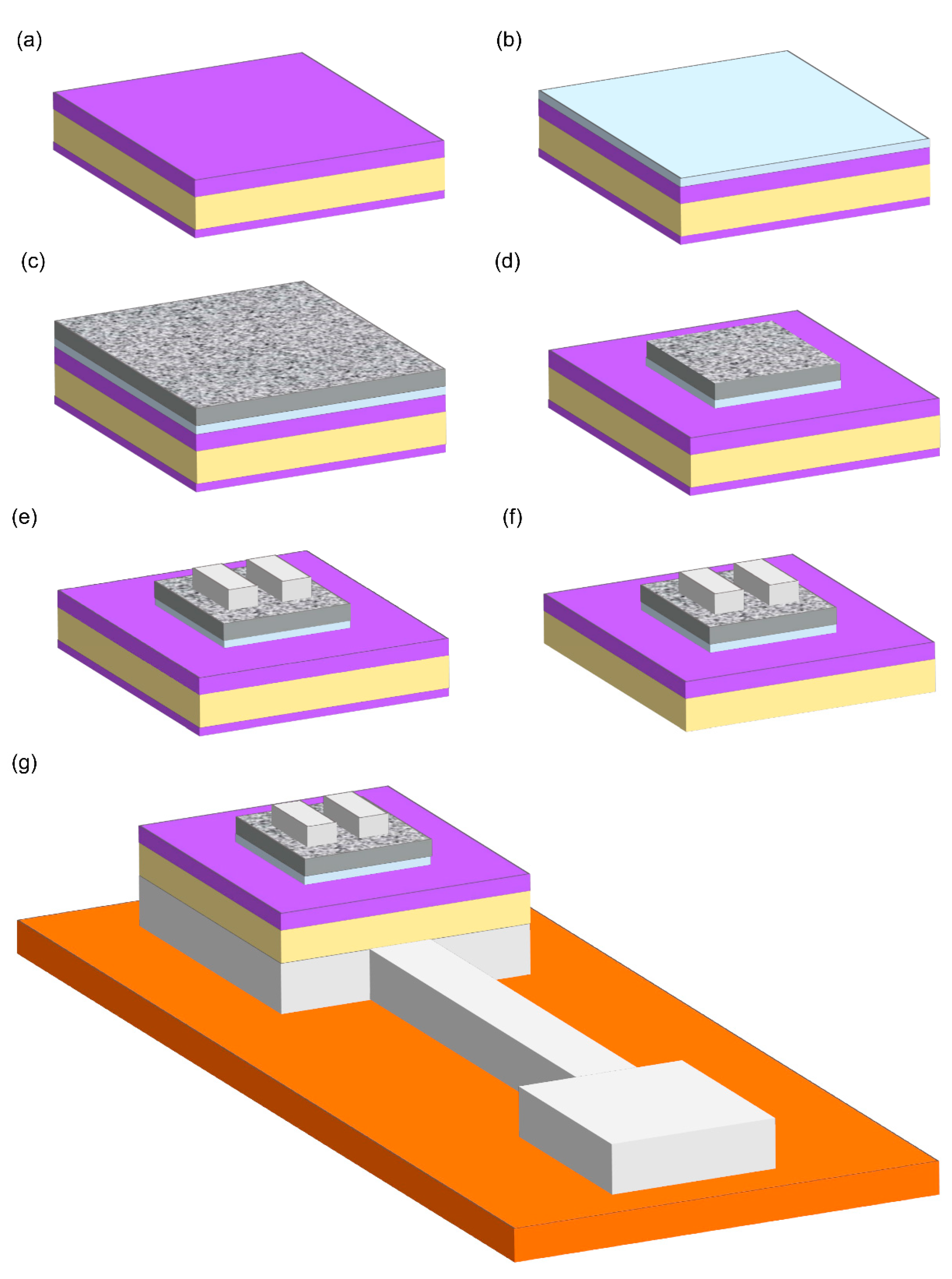
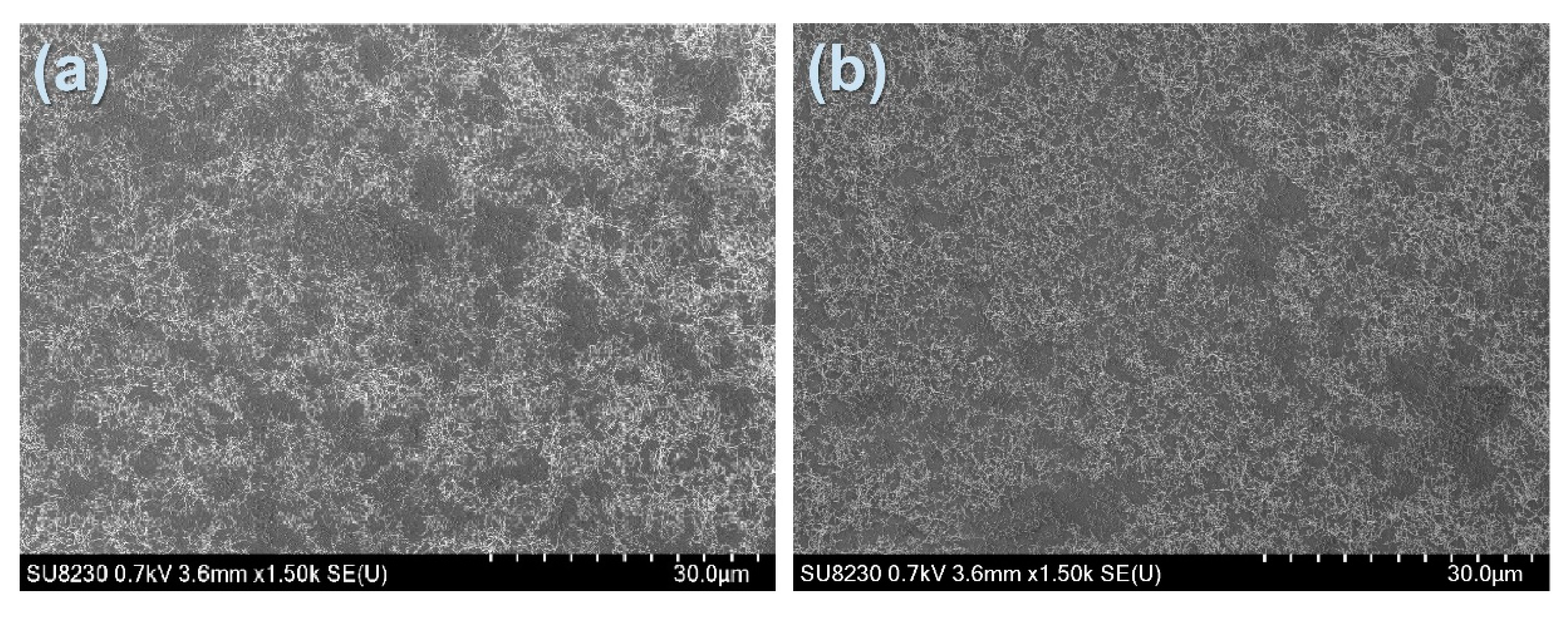
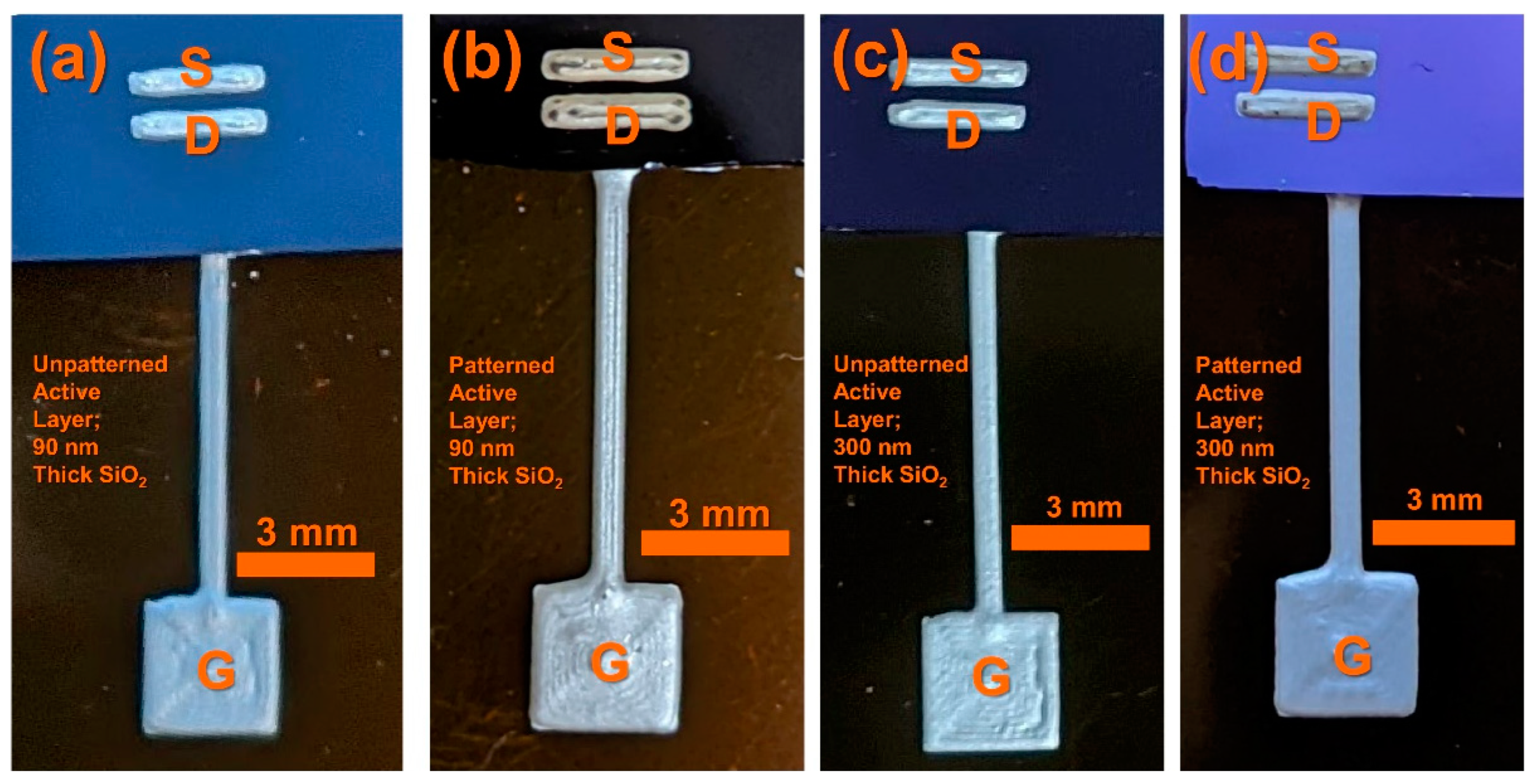
2. Materials and Methods
3. Results
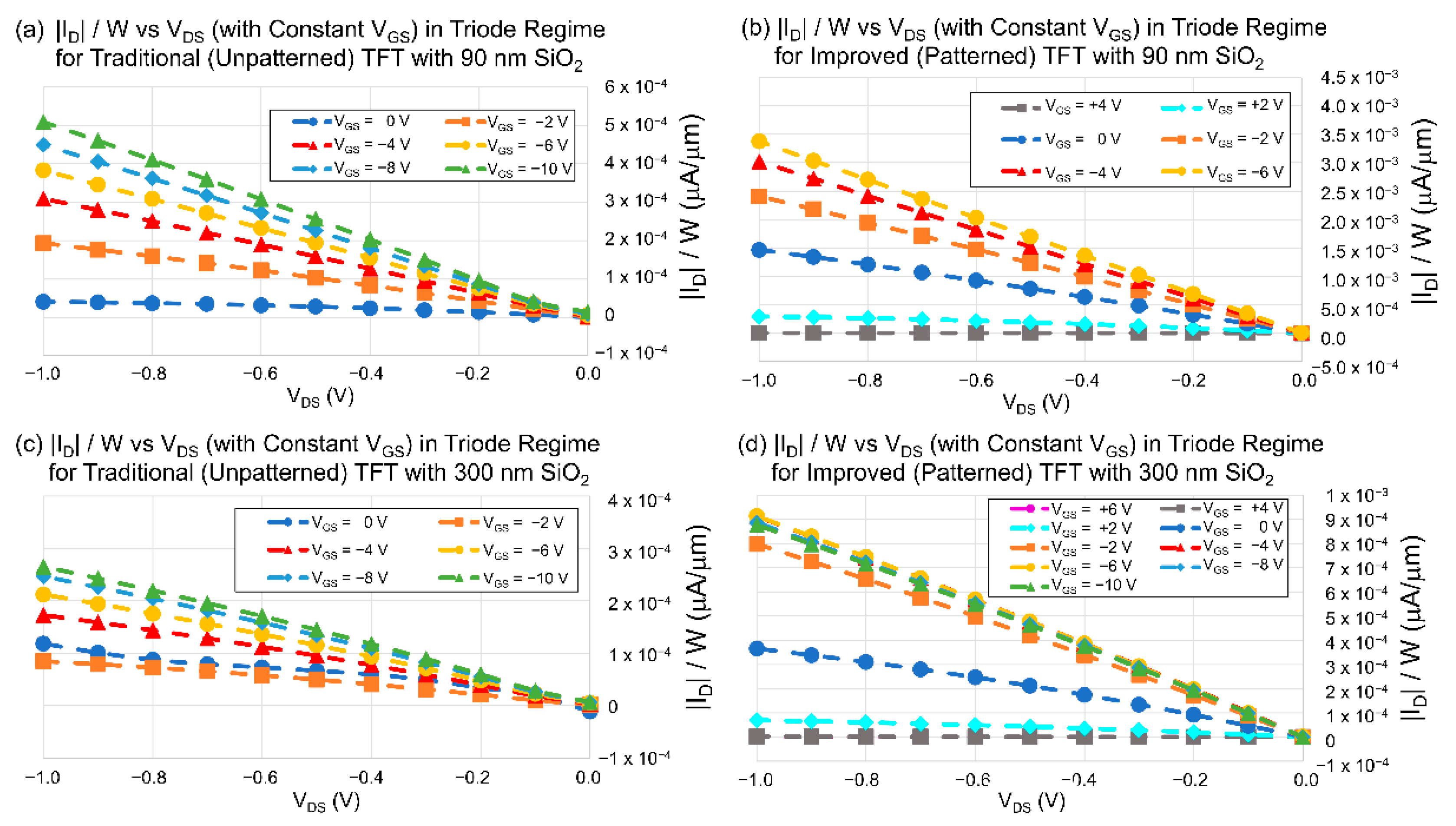
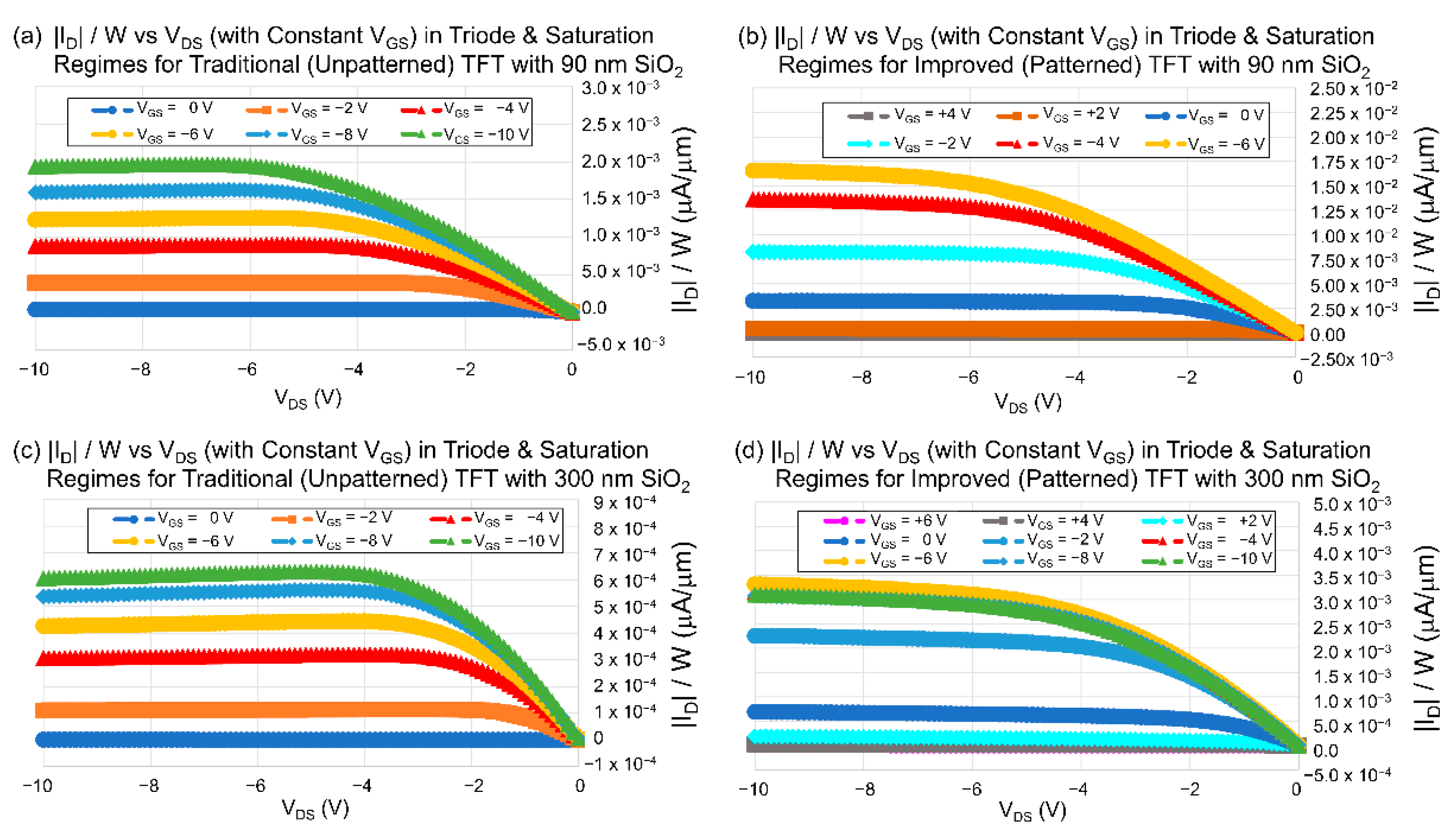
3.1. |ID|/W versus VDS Characteristics:
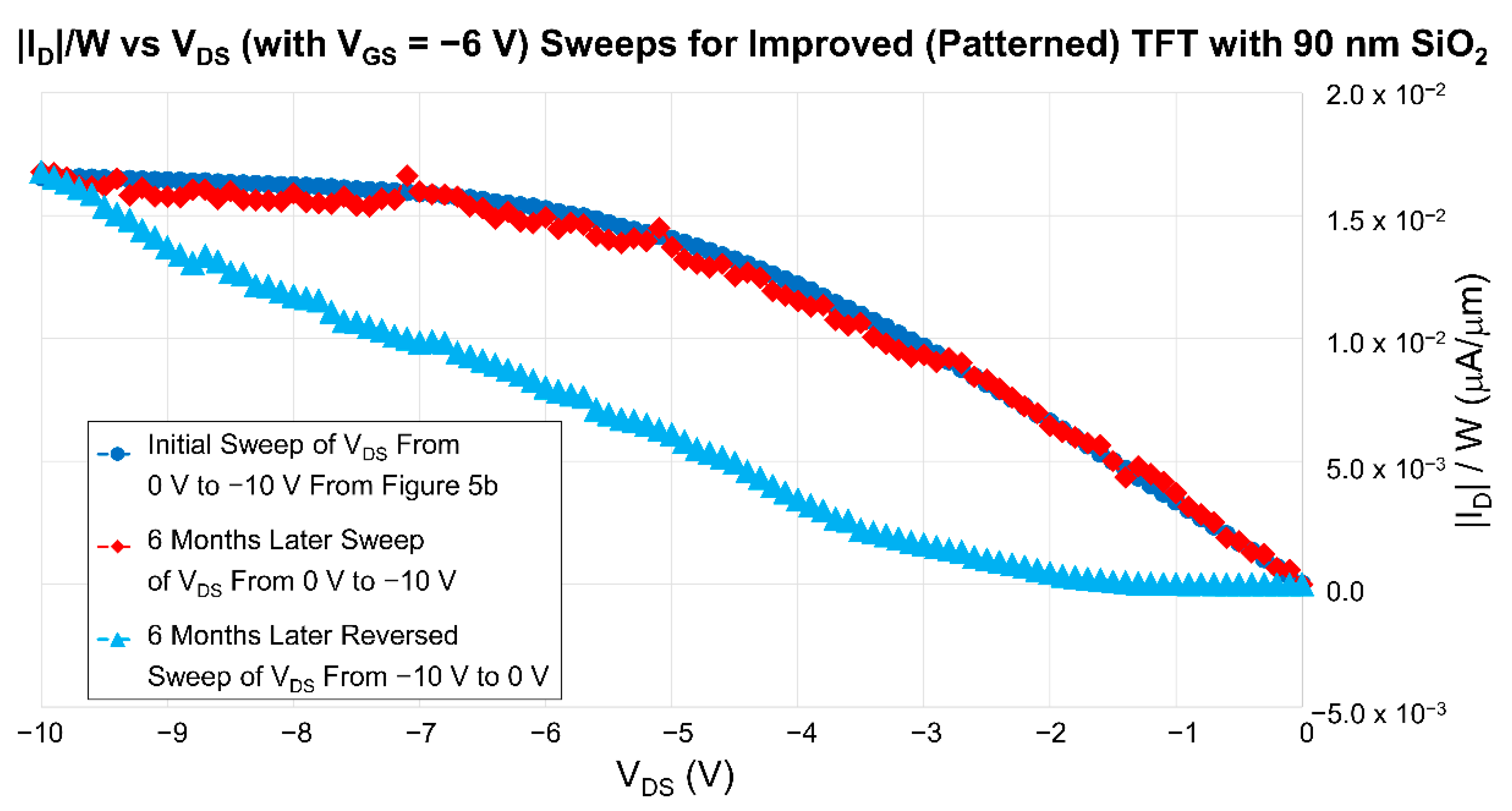
3.2. Repeatability and Hysteresis of |ID|/W versus VDS Measurements
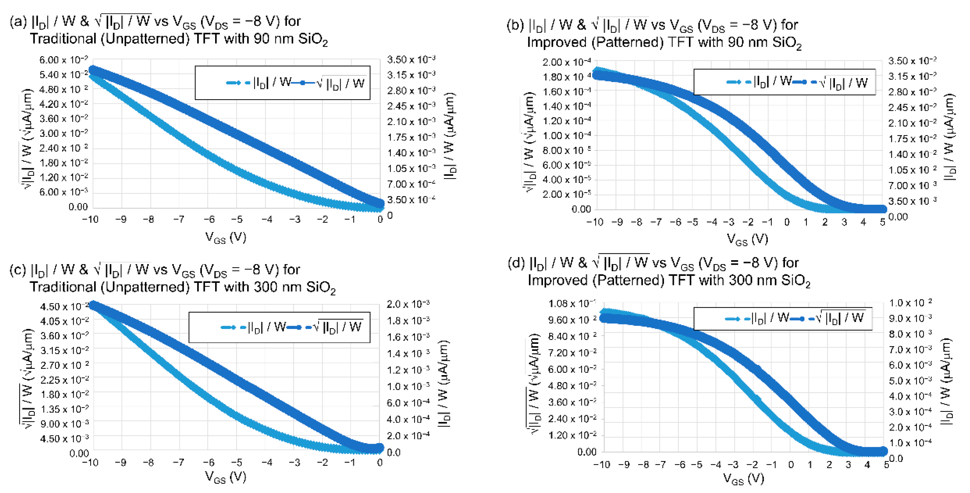
3.3. |ID|/W versus VGS and versus VGS Characteristics:
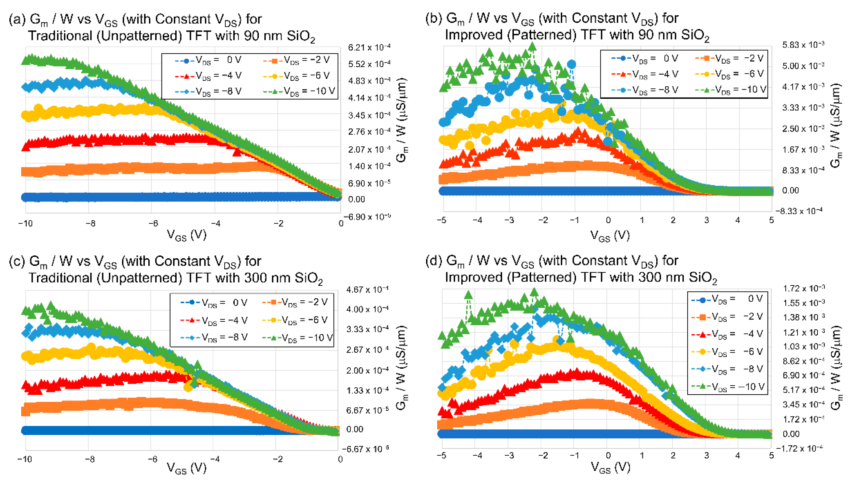
3.4. Gm/W versus VGS Characteristics: Transconductance
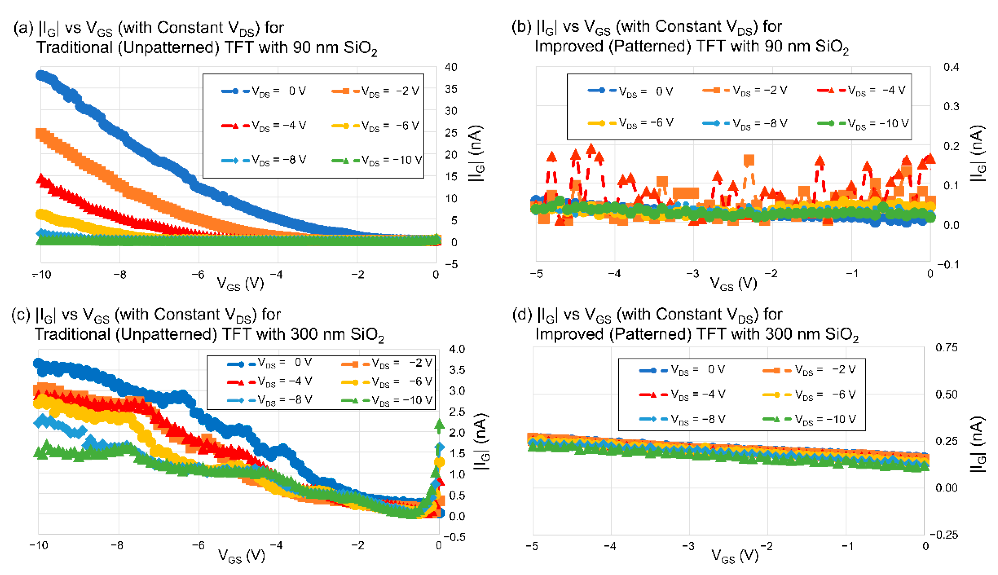
3.5. |IG| versus VGS Characteristics: Resolving Unusual Gate Leakage Current Behavior
4. Discussion
5. Conclusions
Author Contributions
Funding
Institutional Review Board Statement
Informed Consent Statement
Data Availability Statement
Acknowledgments
Conflicts of Interest
References
- Pandey, M.; Rashiku, M.; Bhattacharya, S. Recent progress in the development of printed electronic devices. In Chemical Solution Synthesis for Materials Design and Thin Film Device Applications; Das, S., Dhara, S., Eds.; Elsevier: Amsterdam, The Netherlands, 2021; pp. 349–368. [Google Scholar]
- Nomura, K.; Ohta, H.; Takagi, A.; Kamiya, T.; Hirano, M.; Hosono, H. Room Temperature Fabrication of Transparent Flexible Thin-Film Transistors Using Amorphous Oxide Semiconductors. Nature 2004, 432, 488–492. [Google Scholar] [CrossRef]
- Wang, L.; Yoon, M.-H.; Lu, G.; Yang, Y.; Facchetti, A.; Mark, T.J. High-performance Transparent Inorganic-organic Hybrid Thin-film N-type Transistors. Nat. Mater. 2006, 5, 893–900. [Google Scholar] [CrossRef]
- Nomura, K.; Ohta, H.; Ueda, K.; Kamiya, T.; Hirano, M.; Hosono, H. Thin-film Transistor Fabricated in Single-crystalline Transparent Oxide Semiconductor. Science 2003, 300, 1269–1272. [Google Scholar] [CrossRef]
- Sun, Y.; Rogers, J.A. Inorganic Semiconductors for Flexible Electronics. Adv. Mater. 2007, 19, 1897–1916. [Google Scholar] [CrossRef]
- Madelung, O. (Ed.) Technology and Applications of Amorphous Silicon; Springer: Berlin, Germany, 2000. [Google Scholar]
- Wang, M.-C.; Yang, H.-C.; Hsu, H.-W.; Hsieh, Z.-H.; Chen, S.-Y.; Chang, S.-Y.; Liu, C.-H. Degradation Mechanism for Continuous-Wave Green Laser-crystallized Polycrystalline Silicon n-Channel Thin-Film Transistors under Low Vertical-Field Hot-Carrier Stress with Different Laser Annealing Powers. Jpn. J. Appl. Phys. 2011, 50, 04DH16. [Google Scholar] [CrossRef]
- Cavallari, M.R.; Pastrana, L.M.; Sosa, C.D.F.; Izquierdo, J.E.E.; Fonseca, F.J.; Amorim, C.A.; Kymissis, I. Organic Thin-Film Transistors as Gas Sensors: A Review. Materials 2021, 14, 3. [Google Scholar] [CrossRef]
- Knobelspies, S.; Bierer, B.; Daus, A.; Takabayashi, A.; Salvatore, G.A.; Cantarella, G.; Perez, A.O.; Wöllenstein, J.; Palzer, S.; Tröster, G. Photo-Induced Room-Temperature Gas Sensing with a-IGZO Based Thin-Film Transistors Fabricated on Flexible Plastic Foil. Sensors 2018, 18, 358. [Google Scholar] [CrossRef] [PubMed]
- Elkington, D.; Cooling, N.; Belcher, W.; Dastoor, P.C.; Zhou, X. Organic Thin-Film Transistor (OTFT)-Based Sensors. Electronics 2014, 3, 234–254. [Google Scholar] [CrossRef]
- Rim, Y.S. Review of metal oxide semiconductors-based thin-film transistors for point-of-care sensor applications. J. Inf. Disp. 2020, 21, 203–210. [Google Scholar] [CrossRef]
- Gelinck, G.H.; Huitema, H.E.A.; van Veenendaal, E.; Cantatore, E.; Schrijnemakers, L.; van der Putten, J.B.P.H.; Geuns, T.C.T.; Beenhakkers, M.; Giesbers, J.B.; Huisman, B.-H.; et al. Flexible active-matrix displays and shift registers based on solution-processed organic transistors. Nat. Mater. 2004, 3, 106–110. [Google Scholar] [CrossRef]
- Klauk, H.; Halik, M.; Zschieschang, U.; Eder, F.; Rhode, D.; Schmid, G.; Dehm, C. Flexible organic complementary circuits. IEEE Trans. Electron Devices. 2005, 52, 618–622. [Google Scholar] [CrossRef]
- Wang, C.; Zhang, J.; Ryu, K.; Badmaev, A.; De Arco, L.G.; Zhou, C. A wafer-scale fabrication of separated carbon nanotube thin-film transistors for display application. Nano Lett. 2009, 9, 4285–4291. [Google Scholar] [CrossRef] [PubMed]
- Chen, J.; Kumar, S. Variability in output characteristics of single-walled carbon nanotube thin-film transistors. IEEE Trans. Nanotechnol. 2018, 17, 353–361. [Google Scholar] [CrossRef]
- Takahashi, T.; Takei, K.; Gilles, A.G.; Fearing, R.S.; Javey, A. Carbon nanotube active-matrix backplanes for conformal electronics and sensors. Nano Lett. 2011, 11, 5408–5413. [Google Scholar] [CrossRef] [PubMed]
- Wong, H.-S.P.; Akinwande, D. Carbon nanotube field-effect transistors. In Carbon Nanotube and Graphene Device Physics; Cambridge University Press: New York, NY, USA, 2011; pp. 191–232. [Google Scholar]
- Kumar, S.; Cola, B.A.; Jackson, R.; Graham, S. A Review of Carbon Nanotube Ensembles as Flexible Electronics and Advanced Packaging Materials. J. Electron. Packag. 2011, 133, 020906. [Google Scholar] [CrossRef]
- Sangwan, V.K.; Ortiz, R.P.; Alaboson, J.M.P.; Emery, J.D.; Bedzyk, M.J.; Lauhon, L.J.; Marks, T.J.; Hersam, M.C. Fundamental performance limits of carbon nanotube thin-film transistors achieved using hybrid molecular dielectrics. ACS Nano 2012, 6, 7480–7488. [Google Scholar] [CrossRef]
- Park, S.; Vosguerichian, M.; Bao, Z. A review of fabrication and applications of carbon nanotube film-based flexible electronics. Nanoscale 2013, 5, 1727–1752. [Google Scholar] [CrossRef] [PubMed]
- Rutherglen, C.; Jain, D.; Burke, P. Nanotube electronics for radio frequency applications. Nat. Nanotechnol. 2009, 4, 811–819. [Google Scholar] [CrossRef]
- Vaillancourt, J.; Lu, X.; Han, X.; Janzen, D.C. High-speed thin-film transistor on flexible substrate fabricated at room temperature. Electron. Lett. 2006, 42, 1365–1367. [Google Scholar] [CrossRef]
- Hirotani, J.; Ohno, Y. Carbon Nanotube Thin Films for High-Performance Flexible Electronics Applications. Top. Curr. Chem. 2019, 377, 257–270. [Google Scholar]
- Wang, H.; Luo, J.; Robertson, A.; Ito, Y.; Yan, W.; Lang, V.; Zaka, M.; Schäffel, F.; Rümmeli, M.H.; Briggs, G.A.D.; et al. High-performance field effect transistors from solution processed carbon nanotubes. ACS Nano 2010, 4, 6659–6664. [Google Scholar] [CrossRef]
- Jeong, M.; Lee, K.; Choi, E.; Kim, A.; Lee, S.B. Spray-coated carbon nanotube thin-film transistors with striped transport channels. Nanotechnology 2012, 23, 505203. [Google Scholar] [CrossRef]
- Shimizu, M.; Fujii, S.; Tanaka, T.; Kataura, H. Effects of surfactants on the electronic transport properties of thin-film transistors of single-wall carbon nanotubes. J. Phys. Chem. C 2013, 117, 11744–11749. [Google Scholar] [CrossRef]
- Huang, Q.; Liu, F.; Zhao, J.; Xia, J.; Liang, X. Ambipolarity suppression of carbon nanotube thin film transistors. Carbon 2020, 157, 358–363. [Google Scholar] [CrossRef]
- Xu, J.-L.; Dai, R.-X.; Xin, Y.; Sun, Y.-L.; Li, X.; Yu, Y.-X.; Xiang, L.; Xie, D.; Wang, S.-D.; Ren, T.-L. Efficient and Reversible Electron Doping of Semiconductor-Enriched Single-Walled Carbon Nanotubes by Using Decamethylcobaltocene. Sci. Rep. 2017, 7, 6751. [Google Scholar] [CrossRef] [PubMed]
- Cai, L.; Wang, C. Carbon Nanotube Flexible and Stretchable Electronics. Nanoscale Res. Lett. 2015, 10, 320. [Google Scholar] [CrossRef]
- Kim, Y.-H.; Heo, J.-S.; Kim, T.-H.; Park, S.; Yoon, M.-H.; Kim, J.; Oh, M.S.; Yi, G.-R.; Noh, Y.-Y.; Park, S.K. Flexible Metal-oxide Devices Made by Room-temperature Photochemical Activation of Sol-gel Films. Nature 2012, 489, 128–132. [Google Scholar] [CrossRef]
- Lin, Y.-H.; Faber, H.; Zhao, K.; Wang, Q.; Amassian, A.; McLachlan, M.; Anthopoulos, T.D. High-performance ZnO Transistors Processed via an Aqueous Carbon-free Metal Oxide Precursor Route at Temperatures between 80–180 °C. Adv. Mater. 2013, 25, 4340–4346. [Google Scholar] [CrossRef]
- Lee, J.; Lim, K.-H.; Kim, Y.S. Effects of Unusual Gate Current on the Electrical Properties of Oxide Thin-Film Transistors. Sci. Rep. 2018, 8, 13905. [Google Scholar] [CrossRef]
- Arai, T.; Sasaoka, T. Emergent Oxide TFT Technologies for Next-generation AM-OLED Displays. SID Int. Symp. Dig. Tech. Pap. 2011, 42, 710–713. [Google Scholar] [CrossRef]
- Matsuo, T.; Mori, S.; Ban, A.; Imaya, A. Advantages of IGZO Oxide Semiconductor. SID Int. Symp. Dig. Tech. Pap. 2014, 45, 83–86. [Google Scholar] [CrossRef]
- Nag, M.; Chasin, A.; Rockele, M.; Steudel, S.; Myny, K.; Bhoolokam, A.; Tripathi, A.; der Putten, B.; Kumar, A.; van der Steen, J.-L.; et al. Single-source Dual-layer Amorphous IGZO Thin-film Transistors for Display and Circuit Applications. J. Soc. Inf. Disp. 2013, 21, 129–136. [Google Scholar] [CrossRef]
- Seong, K.; Kim, K.; Park, S.Y.; Kim, Y.S. Micro-patterned ZnO Semiconductors for High Performance Thin Film Transistors via Chemical Imprinting with a PDMS Stamp. Chem. Commun. 2013, 49, 2783–2785. [Google Scholar] [CrossRef] [PubMed]
- Xu, W.; Wang, H.; Ye, L.; Xu, J. The Role of Solution-processed High-κ Gate Dielectrics in Electrical Performance of Oxide Thin Film Transistors. J. Mater. Chem. C. 2014, 2, 5389–5396. [Google Scholar] [CrossRef]
- Sung, S.; Park, S.; Cha, S.; Lee, W.-J.; Kim, C.-H.; Yoon, M.-H. Direct Patterning of Sol–gel Metal Oxide Semiconductor and Dielectric Films via Selective Surface Wetting. RSC Adv. 2015, 5, 38125–38129. [Google Scholar] [CrossRef]
- Lombardo, S.; Stathis, J.H.; Linder, B.P.; Pey, K.L.; Palumbo, F.; Tung, C.H. Dielectric breakdown mechanisms in gate oxides. J. App. Phys. 2005, 98, 12. [Google Scholar] [CrossRef]
- Tai, M.-C.; Wang, Y.-X.; Chang, T.-C.; Huang, H.-C.; Lin, C.-C.; Huang, B.-S.; Chang, H.-Y.; Huang, J.-W.; Sze, S. Gate dielectric breakdown in A-InGaZnO thin film transistors with Cu electrodes. IEEE Electron Device Lett. 2021, 42, 851–854. [Google Scholar] [CrossRef]
- Chen, P.; Fu, Y.; Aminirad, R.; Wang, C.; Zhang, J.; Wang, K.; Galatsis, K.; Zhou, C. Fully Printed Carbon Nanotube Thin Film Transistor Circuits and Its Application in Organic Light Emitting Diode Control. Nano Lett. 2011, 11, 5301–5308. [Google Scholar] [CrossRef]
- Jang, S.; Jang, H.; Lee, Y.; Suh, D.; Baik, S.; Hong, B.H.; Ahn, J.-H. Flexible, transparent single-walled carbon nanotube transistors with graphene electrodes. Nanotechnology 2010, 21, 425201. [Google Scholar] [CrossRef]
- Zhao, J. Structures and fabrication of TFTs. In Printed Electronics: Materials, Technologies and Applications; Cui, Z., Ed.; Wiley: Singapore, 2016; pp. 157–159. [Google Scholar]
- Antoniou, M.; Tsounidi, D.; Petrou, P.S.; Beltsios, K.G.; Kakabakos, S.E. Functionalization of silicon dioxide and silicon nitride surfaces with aminosilanes for optical biosensing applications. Med. Devices Sens. 2020, 3, e10072. [Google Scholar] [CrossRef]
- Howarter, J.A.; Youngblood, J.P. Optimization of silica silanization by 3-aminopropyltriethoxysilane. Langmuir 2006, 22, 11142–11147. [Google Scholar] [CrossRef] [PubMed]
- Fortunato, E.M.C.; Barquinha, P.M.C.; Pimentel, A.C.M.B.G.; Gonçalves, A.M.F.; Marques, A.J.S.; Pereira, L.M.N.; Martins, R.F.P. Fully Transparent ZnO Thin-film Transistor Produced at Room Temperature. Adv. Mater. 2005, 17, 590–594. [Google Scholar] [CrossRef]
- Bashir, A.; Wöbkenberg, P.H.; Smith, J.; Anthopoulos, T. High-performance Zinc Oxide Transistors and Circuits Fabricated by Spray Pyrolysis in Ambient Atmosphere. Adv. Mater. 2009, 21, 2226–2231. [Google Scholar] [CrossRef]
- Adamopoulos, G.; Thomas, S.; Wöbkenberg, P.H.; Bradley, D.D.C.; McLachlan, M.A.; Anthopoulos, T.D. High-mobility Low-voltage ZnO and Li-doped ZnO Transistors Based on ZrO2 High-k Dielectric Grown by Spray Pyrolysis in Ambient Air. Adv. Mater. 2011, 23, 1894–1898. [Google Scholar] [CrossRef]
- Liu, J.; Casavant, M.J.; Cox, M.; Walters, D.A.; Boul, P.; Lu, W.; Rimberg, A.J.; Smith, K.A.; Colbert, D.T.; Smalley, R.E. Controlled deposition of individual single-walled carbon nanotubes on chemically functionalized templates. Chem. Phys. Lett. 1999, 303, 125–139. [Google Scholar] [CrossRef]
- Romanuik, S.F.; Rout, B.; Girard-Lauriault, P.-L.; Bhadra, S. Resolving Unusual Gate Current and Dielectric Breakdown of Solution Processed Carbon Nanotube Thin Film Transistor. In Proceedings of the IEEE Internation Symposium on Circuits and Systems 2022 (ISCAS 22) Conference, Austin, TX, USA, 28 May–1 June 2022. [Google Scholar]
- Han, K.N.; Li, C.A.; Bui, M.-P.N.; Seong, G.H. Patterning of Single-Walled Carbon Nanotube Films on Flexible, Transparent Plastic Substrates. Langmuir 2010, 26, 598–602. [Google Scholar] [CrossRef] [PubMed]
- Buendía, J.J.; De Cea, M.; Luan, J. Determination of the Field-Effect Mobility and the Density of States of a Thin-Film Transistor; Universitat Politècnica de Catalunya Barcelona Tech UPCommons: Barcelona, Spain; Available online: https://upcommons.upc.edu/bitstream/handle/2117/192490/otft1.pdf?sequence=1&isAllowed=y (accessed on 20 February 2022).
- LeMieux, M.C.; Sok, S.; Roberts, M.E.; Opatkiewicz, J.P.; Liu, D.; Barman, S.N.; Patil, N.; Mitra, S.; Bao, Z. Solution Assembly of Organized Carbon Nanotube Networks for Thin-Film Transistors. ACS Nano 2009, 3, 4089–4097. [Google Scholar] [CrossRef] [PubMed]
- Wang, H.; Wei, P.; Li, Y.; Han, J.; Lee, H.R.; Naab, B.D.; Liu, N.; Wang, C.; Adijanto, E.; Tee, B.C.-K.; et al. Tuning the threshold voltage of carbon nanotube transistors by n-type molecular doping for robust and flexible complementary circuits. Proc. Natl. Acad. Sci. USA 2014, 111, 4776–4781. [Google Scholar] [CrossRef]


| TFT | SWCNT Layer Patterned? | SiO2 Thickness tox (nm) | Length of S and D Electrodes (mm) | Width of S and D Electrodes (μm) | Separation between S and D Electrodes (μm) | Channel Width W (mm) | Channel Length L (μm) |
|---|---|---|---|---|---|---|---|
| Traditional TFT 1 * | Unpatterned | 90 | 5.4 | 840 | 320 | 5.4 | 320 |
| Improved TFT 1 * | Patterned | 300 | 6.3 | 835 | 370 | 6.3 | 370 |
| Traditional TFT 2 | Unpatterned | 90 | 2.9 | 630 | 320 | 2.9 | 320 |
| Improved TFT 2 | Patterned | 90 | 3.0 | 660 | 290 | 3.0 | 290 |
| Traditional TFT 3 | Unpatterned | 300 | 3.0 | 600 | 350 | 3.0 | 350 |
| Improved TFT 3 | Patterned | 300 | 2.9 | 610 | 330 | 2.9 | 330 |
| TFT | SWCNT Layer Patterned? | SiO2 Thickness tox (nm) | On-State Current |ION|/W (μA/μm) | Off-State Current |IOFF|/W (μA/μm) | On/off Ratios ION/IOFF (A/A) | Ratio of Improved TFT on/off Ratio/Traditional TFT on/off Ratio |
|---|---|---|---|---|---|---|
| Traditional TFT 1 * | Unpatterned | 90 | Indeterminable Due to Dielectric Breakdown | Indeterminable Due to Dielectric Breakdown | Indeterminable Due to Dielectric Breakdown | -- |
| Improved TFT 1 * | Patterned | 300 | 7.97 × 10⁻⁵ | 3.02 × 10⁻⁸ | 2,640 | -- |
| Traditional TFT 2 | Unpatterned | 90 | 1.23 × 10⁻³ | 6.38 × 10⁻⁸ | 19,280 | -- |
| Improved TFT 2 | Patterned | 90 | 1.65 × 10⁻² | 6.8 × 10⁻⁸ | 242,650 | 12.59 |
| Traditional TFT 3 | Unpatterned | 300 | 6.07 × 10⁻⁴ | 3.33 × 10⁻⁸ | 18,230 | -- |
| Improved TFT 3 | Patterned | 300 | 3.29 × 10⁻³ | 1.09 × 10⁻⁷ | 30,180 | 1.66 |
| TFT | SWCNT Layer Patterned? | SiO2 Thickness tox (nm) | Threshold Voltage Vth (V) | Charge Carrier Mobility μ (cm2 V−1 s−1) | Ratio of Improved TFT μ/Traditional TFT μ |
|---|---|---|---|---|---|
| Traditional TFT 1 * | Unpatterned | 90 | Indeterminable Due to Dielectric Breakdown | Indeterminable Due to Dielectric Breakdown | -- |
| Improved TFT 1 * | Patterned | 300 | −1.5 | 0.3 | -- |
| Traditional TFT 2 | Unpatterned | 90 | +1.96 | 0.51 | -- |
| Improved TFT 2 | Patterned | 90 | +2.63 | 7.82 | 15.3 |
| Traditional TFT 3 | Unpatterned | 300 | −1.73 | 1.48 | -- |
| Improved TFT 3 | Patterned | 300 | +3.43 | 8.10 | 5.47 |
| TFT | SWCNT Layer Patterned? | SiO2 Thickness tox (nm) | Gate Current |IG| (with VDS = 0 V) | Ratio of Improved TFT |IG|/Traditional TFT |IG| |
|---|---|---|---|---|
| Traditional TFT 1 * | Unpatterned | 90 | 3.5 μA | -- |
| Improved TFT 1 * | Patterned | 300 | 420 pA | 8,330 |
| Traditional TFT 2 | Unpatterned | 90 | 10 nA | -- |
| Improved TFT 2 | Patterned | 90 | 60 pA | 170 |
| Traditional TFT 3 | Unpatterned | 300 | 2.1 nA | -- |
| Improved TFT 3 | Patterned | 300 | 260 pA | 8 |
Publisher’s Note: MDPI stays neutral with regard to jurisdictional claims in published maps and institutional affiliations. |
© 2022 by the authors. Licensee MDPI, Basel, Switzerland. This article is an open access article distributed under the terms and conditions of the Creative Commons Attribution (CC BY) license (https://creativecommons.org/licenses/by/4.0/).
Share and Cite
Romanuik, S.F.; Rout, B.; Girard-Lauriault, P.-L.; Bhadra, S. Resolving the Unusual Gate Leakage Currents of Thin-Film Transistors with Single-Walled Carbon-Nanotube-Based Active Layers. Electronics 2022, 11, 3719. https://doi.org/10.3390/electronics11223719
Romanuik SF, Rout B, Girard-Lauriault P-L, Bhadra S. Resolving the Unusual Gate Leakage Currents of Thin-Film Transistors with Single-Walled Carbon-Nanotube-Based Active Layers. Electronics. 2022; 11(22):3719. https://doi.org/10.3390/electronics11223719
Chicago/Turabian StyleRomanuik, Sean F., Bishakh Rout, Pierre-Luc Girard-Lauriault, and Sharmistha Bhadra. 2022. "Resolving the Unusual Gate Leakage Currents of Thin-Film Transistors with Single-Walled Carbon-Nanotube-Based Active Layers" Electronics 11, no. 22: 3719. https://doi.org/10.3390/electronics11223719
APA StyleRomanuik, S. F., Rout, B., Girard-Lauriault, P.-L., & Bhadra, S. (2022). Resolving the Unusual Gate Leakage Currents of Thin-Film Transistors with Single-Walled Carbon-Nanotube-Based Active Layers. Electronics, 11(22), 3719. https://doi.org/10.3390/electronics11223719