1. Introduction
Conventional carrier-based sinusoidal PWM (SPWM) and space vector PWM(SV-PWM)are the two most popular high switching frequency (HSF) approaches. Low switching frequency (LSF) approaches include space vector modulation (SVM) and selective harmonic removal.
In addition, to enhance the effective switching frequency in classic carrier-based SPWM for industrial applications, phase shifting is typically used with HSF.
The SVM strategy is another interesting method that has been used in three-level converters. LSFs often accomplish one or two commutations of the semiconductor devices to develop a multilevel waveform across one period of output voltages. These techniques have such applications as space vector control and selective harmonic removal.
Another method for solving transcendental equations for angles of switches has recently been established. Polynomial equations can be converted from transcendental equations that characterize harmonic content. Specific odd harmonics have been eliminated utilizing consequent elimination theory. However, if the number of DC voltages or switching angles rises, these equation’s degrees become too large to solve using elimination theory, which is a limitation of today’s computer algebra software tools.
Reduced common mode voltages, high voltage capability, low dV/dt, close to sinusoidal responses, and little or no response filter make multilevel inverters ideal for high-power applications [
1].
ZS/qZSCMIs alleviate the disadvantages of traditional CMIs by integrating the ZS/qZS network with the H-bridge module due to the buck/boost and single stage inversion of the Z source (ZS)/quasi-Z source (qZS) inverter.
There are two operating states for typical H-bridge modules in CMI: active and zero. However, operating states for ZS/qZS-CMI are a little more complicated due to additional shoot-through stages while evaluating inverter efficiency [
2,
3].
Lower-order harmonics, as well as modified sinusoidal output voltage, can be avoided or decreased using PWM approaches.
The number of necessary bidirectional switches is eight, which is smaller than all other topologies except the new hybrid asymmetric H-bridge multilevel inverter (NHAH-MLI), which has a major drawback of voltage balancing due to asymmetric capacitors. CHB-MLI does not require any unidirectional switches, which is also a benefit. In comparison to the other topologies addressed, the switching operation in CHB-MLI is likewise relatively easy. The possibility of adding a separate DC source or photovoltaic (PV) string to CHB-MLI boosts its versatility.
The CHB-MLI has improved THD, according to the topological analysis of multilevel inverters. Because there are fewer switching devices, there is a lower danger of failure. For photovoltaic (PV) applications, the cascaded H-bridge MLI appears to have more promise.
A simulation was carried out for the seven-level qZS-CHBMLI with SPV as a source at each H-bridge due to the presence of the “Z” network between the PV source and the H-bridge converter. Due to the presence of a “Z” network between the PV source and the H-bridge converter, the qZS-CHBMLI has a continuous current characteristic. Because it operates in the shoot-through state, it will not help reduce the output voltage. A lower THD is associated with a higher modulation index. As a result, it can be concluded that qZSCHBMLI is suitable for photovoltaic applications.
The analysis of a solar photovoltaic system, as well as the design of a stand-alone SPV system, was carried out in this research paper.
This paper is divided into seven sections. The first section is the introduction, the second section focuses on modulation strategies, and the third section describes the different multilevel inverters’ topologies and comparison and balance-control problems in multilevel inverters. Section four discusses the performance of basic MLI topologies using MATLAB/Simulink. The fifth and sixth sections focus on modeling and analyzing SPV-based quasi-Z-source cascaded H-bridge (qZSCHBMLI) with the best switching (phase shift) and best MLI topology (CHB-MLI) using MATLab/Simulink, respectively. Section seven contains the results and discussion. Section eight presents the conclusion of this work.
2. Modulation Strategies
High-frequency switching methods have many commutations for the power semiconductors of the fundamental output voltage in one cycle.
Figure 1 depicts the classification of various approaches based on the switching frequency of multilevel inverters [
4].
2.1. PWM Space Vector
Modulation is a technique for controlling motor devices that is very new and widely used. The output voltage is estimated in the SVPWM approach by utilizing the three response vectors in the inverter’s space vector diagram that are closest to the nodes of the triangle containing the reference vector. The key benefit of this method is that it produces lower THD in output currents and voltages [
5].
2.2. Sinusoidal PWM Techniques (Multicarrier)
The carrier signal in multicarrier PWM systems is a triangle wave as shown in
Figure 2 for the different carrier arrangements, while the reference wave is a sinusoidal signal.
The unipolar switched inverter generates less EMI and offers reduced switching losses, and is beneficial from the efficiency point of view.
When the amplitude modulation index (m
a) is more than unity, over modulation occurs. It causes the creation of lower-order harmonics, which reduces the number of pulses in the line to line voltage waveform. Moreover, the pulse width tends to disappear in the middle of the positive and negative half cycles. The switching operations of the device, as well as the minimum notch and pulse widths, must be preserved. A temporary spike in load current will occur whenever the minimum width notches and pulses are eliminated [
6].
2.3. Selective Harmonic Elimination (SHE)
The basic switching frequency approach, and hence the notion of harmonic elimination, underpins the SHE technique.
Unipolar PWM and bipolar PWM could be needed for multilevel appropriateness when modulation indices are too low. Low modulation indices can also benefit from virtual stage PWM, which provides a viable low modulation index control alternative to unipolar PWM and bipolar PWM.
For SHE methodologies like the virtual stage PWM technique and the fundamental switching frequency technique, the transcendental equation for switching angles is a serious issue [
5].
2.4. Space Vector PWM at Fundamental Frequency
For each state, the SVPWM determines the constant switching time. This SVPWM might simply be set to a greater value. SVPWM effectively utilizes the DC link voltage, has a low current ripple, and is reasonably simple to implement in hardware using DSP [
7].
In comparison to SPWM, SVPWM has a 15% higher voltage consumption ratio. The number of duplicate switching states and the difficulty of picking switching states grows in tandem with the number of levels.
As shown in
Table 1, for each cycle, each sector has seven different switching states (000 and 111 counts as a single state). It has a zero vector at the beginning (for 000) and the end (for 111). Even numbers travel clockwise, whereas odd numbers travel counterclockwise in each sector.
Because of these merits, it is favorable for converter switching control, but a demerit of this method is that it will become more difficult to achieve as the number of levels increases. In addition, this strategy is not capable of completely reducing low-order harmonics (LOH) [
8].
An inverter’s output should ideally be a sinusoidal voltage. Practical inverter outputs, on the other hand, are non-sinusoidal and can be separated into fundamental and harmonic components. THD is commonly used to evaluate inverter performance [
9].
At various m
a values, analysis of total harmonic distortion (THD) was performed using numerous SPWM techniques, such as POD, APOD, PD, and PS, for the modulation indices 0.8, 0.9, and 1.
Figure 3a,b demonstrate a graphical examination of THD vs. modulation indices for unipolar and bipolar modes, respectively.
Therefore, it is proven that at different value of modulation index (m
a), the phase shift technique is best for switching, as shown in
Figure 4.
3. Topologies of Multilevel Inverters (MLIs)
The topologies of MLIs are classified into two types:
Basic topologies
- ◦
diode-clamped multilevel inverter (DC-MLI)
- ◦
flying-capacitor multilevel inverter (FC-MLI)
- ◦
cascaded H-bridge multilevel inverter (CHB-MLI)
Hybrid topologies
- ◦
asymmetric hybrid multilevel inverter (AH-MLI):
- ◦
new symmetrical hybrid multilevel inverter (NSH-MLI)
- ◦
hybrid clamped multilevel inverter (HC-MLI)
3.1. Diode-Clamped Multilevel Inverter (DC-MLI)
Figure 5 depicts an MLI with four capacitors on the DC line and a five-level diode clamp (C
1, C
2, C
3, & C
4). Through clamping diodes for DC-bus voltage V
dc, the voltage stress of each device is fixed to a capacitor voltage level of V
dc/4 [
5].
In each leg, four parallel switch pairs are installed. The parallel switch pairs are set up in such a way that turning on one prevents the other from turning on. (S
1, S
1′), (S
2, S
2′), (S
3, S
3′), and (S
4, S
4′) are the four parallel pairs in this scenario. Reverse voltage clamping diodes must have different voltage ratings, despite the fact that any working switching device only has to block a voltage level of V
dc/(m–1) [
10].
3.2. Flying-Capacitor Multilevel Inverters (FC-MLI)
Figure 6 depicts a basic flying-capacitor MLI. The device voltage is clamped to one capacitor voltage level by independent capacitors, which is why it is termed a flying-capacitor inverter [
11].
The flexibility of voltage combination in a five-level capacitor-clamped multilevel inverter is more with respect to a neutral-point clamped inverter. The output voltage across leg “a” and neutral-point “n” of the five-level MLI can be examined using various switching combinations.
In the previous analysis, the capacitors with negative signals were assumed to be charging and those with positive signs to be discharging. It is manageable to control the charge of a capacitor by using the right capacitor combinations. To clamp the voltage, capacitor clamping inverters, like diode clamping inverters, require a higher number of high-rated capacitors.
An m-level inverter requires a total of (m–1) (m–2)/2 clamping capacitors per leg, in addition to the main DC-line capacitors, assuming that the voltage rating of each essential capacitor is the same as the main power switch [
5].
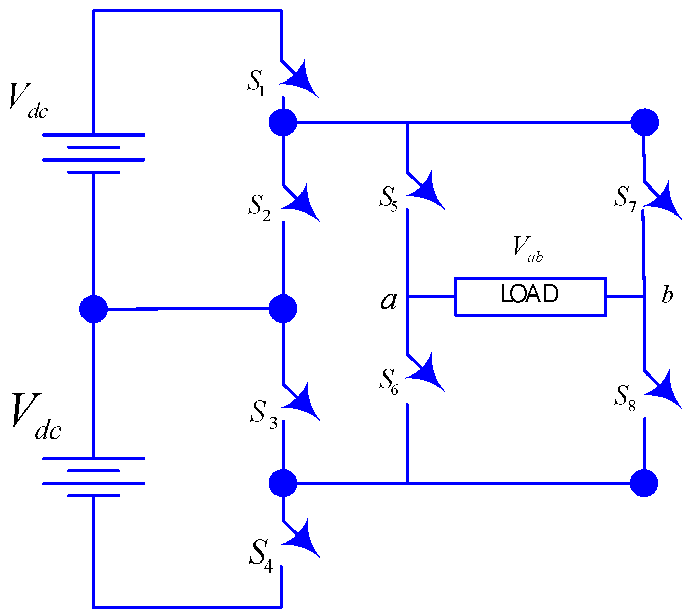
3.3. Cascaded H-Bridge Multilevel Inverters (CHB-MLI)
The output waveforms of cascaded H-bridge multilevel inverters (CHB-MLI) are combined by connecting the AC terminals of two-level bridges in series. The circuit arrangement for a five-level H-bridge MLI with two cascaded cells is shown in
Figure 7. The CMLI relies on a variety of DC sources, including batteries, fuel cells, and solar cells.
Five alternative voltage outputs, +Vdc/2, Vdc, 0, −Vdc/2, and −Vdc, may be formed by altering the patterns of each cell’s four switches and each inverter level. Combining the inverter outputs yields the AC output voltage and n = 2N+1 is the number of output voltage levels, where N is the number of DC sources.
Although the cascaded architecture necessitates a large number of independent DC sources, batteries or PV panels can be utilized to link them in some systems. This sort of inverter without the need of a transformer has been utilized, and its efficiency is greatly improved due to the lack of filters [
12].
3.4. Asymmetric Hybrid Multilevel Inverter (AH-MLI)
The DC voltages of each cell in cascaded MLI are the same. However, it is possible for the cells to have different voltage values [
13], and that type of circuit is known as asymmetric hybrid MLI.
Figure 8 shows two different DC-line levels, one low voltage and the other high voltage. Low-voltage switches, such as IGBT, are S
1–S
4, whereas high-voltage switches, such as GTO, are S
11–S
41. Utilizing unequal DC voltages, the voltage levels can be increased without increasing the number of bridge cells in the inverter circuit. This results in multilevel waveform for similarly used devices. [
14].
In this case, voltage levels are only dependent upon the availability of the DC sources. This property permits the creation of output voltage with higher levels, and due to this increase in level, harmonics will be reduced and thus the obtained voltage has less THD.
Inverter topology is depicted in
Figure 8, in which the input DC voltages of the H-bridge inverter are unequal. The DC voltages for the first and second H-bridges are V
dc and 2V
dc, respectively, in this configuration, and3V
dc, 2V
dc, V
dc, 0,–V
dc,–2V
dc, and–3V
dc are the output voltage levels that the two legs of the inverter can generate. The DC voltage of the second H-bridge is three times that of the first H-bridge in a nine-level inverter. By replacing the second H-bridge output voltage of V
o2 =±2 V
dc with V
o2 = ±3 V
dc and then evaluating the inverter output voltage, all nine output voltage levels can be achieved [
15].
Using dissimilar DC voltages, there are some limitations reported with the CHB MLI. The benefits of the flexible topology are no longer available. Because of the absence of repetitive switching states, the switching strategy becomes substantially more difficult [
14]. Due to this limitation of asymmetric MLI topology, it only suits industrial requirements, though it is feasible—with the equal voltage level among them—to implement high-frequency PWM for the first H-bridge, and at a lower rate for the other switches.
3.5. New Symmetrical Hybrid Multilevel Inverters (NSH-MLI)
It is possible to construct a voltage waveform between points a and b using a certain switching strategy for switches S
1–S
4 and the H-bridge switches.
Figure 9 depicts the operation of a five-level multilevel inverter. The single-leg switches reject voltages of the magnitude V
dc and use a specific modulation mechanism to function at a high frequency. The higher-voltage2V
dc will not flow through the H-bridge switches S
5, S
6, S
7, or S
8 [
16].
Because the output voltage is only half-cycled, these switches only activate every half-cycle. As a result, they operate at a lower frequency while commuting at 0 voltage [
16], and thus this MLI could also be chosen among the hybrid MLIs [
15,
16].
This is accomplished by wiring switches S
5–S
8 as a full-bridge inverter, which is responsible for switching the load terminals in relation to the gate’s output. Negative and positive voltages are produced by turning on the pairings S
5, S
8, and S
6, S
7 in that order. To provide a certain load voltage, the three-level DC–DC converter switches S
1–S
4 are modulated and switched.
Figure 9 depicts a five-level symmetrical hybrid MLI with high-frequency switches S
1 through S
4 rated for half the DC-link voltage E. S
5–S
8 switches are rated with a total DC-link voltage of 2V
dc. Low-frequency switches could be used to build switches S
5–S
8 for GTOs, IGCTs, and other applications because they have the property of only switching once per load-voltage interval when the voltage is zero. On the basis of this technique, this inverter is a symmetric (same DC sources) hybrid (multiple carrier frequencies) MLI. The number of steps in the staircase waveform can be extended by cascading or merging various H-bridge inverters, much like in other examples of cascaded inverters.
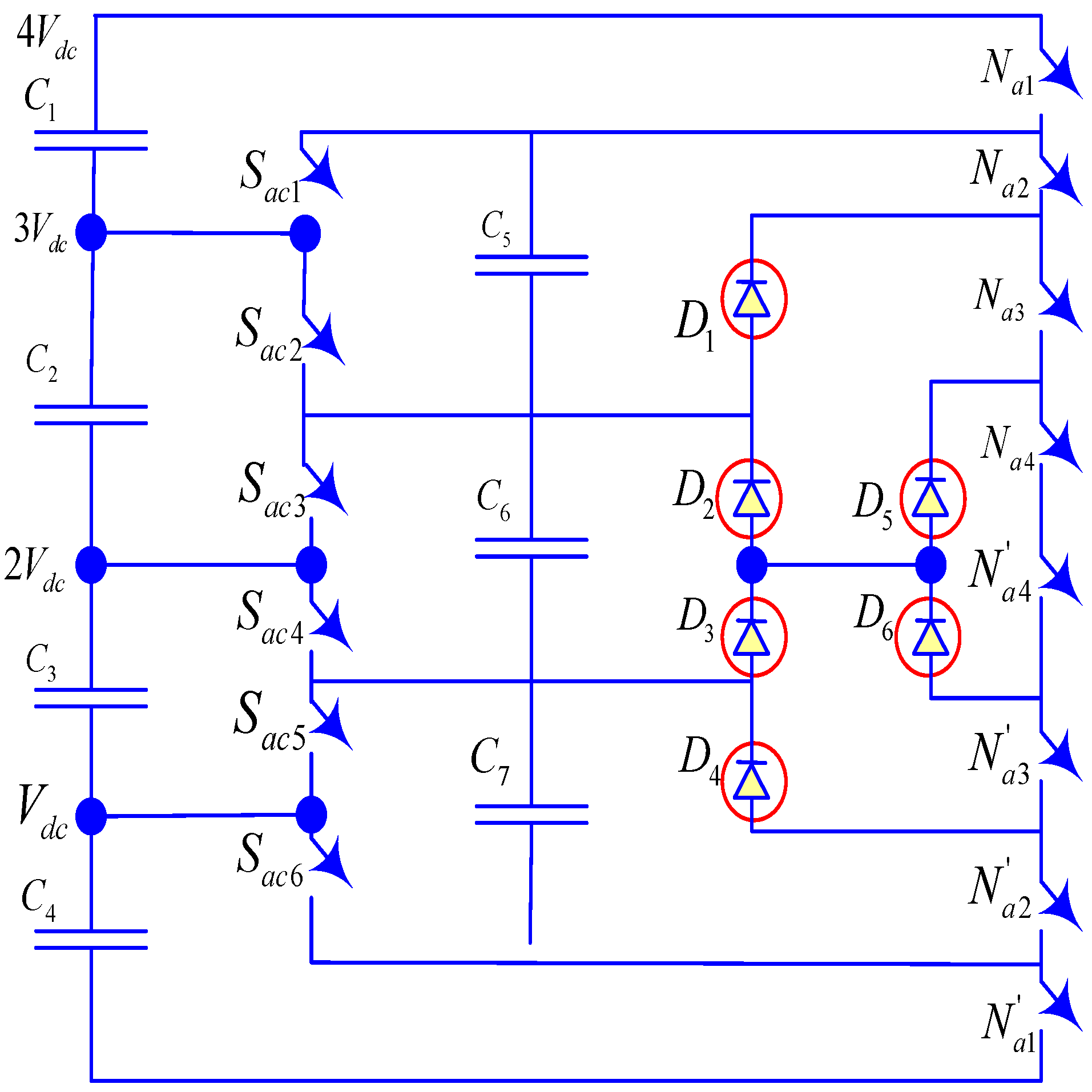
3.6. Hybrid Clamped Multilevel Inverter (HC-MLI)
Figure 10 depicts one leg of the five-level hybrid clamped MLI system [
15]. This self-voltage-balancing architecture is explored by [
17]. The upper switches (N
a1, N
a2, N
a3, andN
a4) are in duality with lower switches (N
a1′, N
a2′, N
a3′, andN
a4′), and switch N
a1 complements switch S
ac1 [
18].
The neighboring switches and the clamped switches S
ac1–S
ac6 are complementary to each other. Switching from one device switching mode to another achieves self-voltage balancing in capacitors [
18].
3.7. Analysis of Components Required for Various Topologies
An inverter with fewer switches leads to reduced power loss, is cost-effective, and reduced switching loss, and is reliable. Therefore, a comparison is made for the components required in various topologies of multilevel inverters. As per
Table 2, CHB-MLI contains fewer switches than other topologies, and thus it is superior to other MLIs. In
Table 3, performance parameters and output levels of the different inverters are shown and compared.
3.8. Complexity in MLI Balance Control
The balanced voltages needed for actual power transformation cannot be achieved with the neutral-point clamped (NPC) MLI without a performance penalty in output voltage. To make voltage balancing easier, neutral-point clamped MLI should be adjusted for reactive and harmonic compensation. To address the issue of imbalanced voltage, a back-to-back converter system and precise voltage-balancing control can be utilized. Also, with the help of extra voltage-balancing circuits, the complexity of voltage balancing can be sorted out. DC choppers can also be used as an additional voltage-balancing circuit [
43].
The flying-capacitor-clamped MLI is generally applied for high-voltage DC/DC conversions. For such requirements, when the load current is DC, the balancing of voltage can be easily achieved. Voltage balancing is more challenging with flying-capacitor-clamped MLIs, since they cannot have self-balanced voltage when modified for reactive power conversion.
Each H-bridge inverter needs its own DC supply in cascaded H-bridge MLI. This MLI is costs less, has greater performance and lower electromagnetic interference, and is more efficient than the conventional PWM inverters for power-conditioning requirements. The CHB-MLI is suitable for overall power conditioning. CHB-MLI has an inbuilt self-voltage-balancing feature, but a marginal voltage imbalance could take place because of the losses in network devices and restricted controller resolution. A method that promises balancing control of DC voltage could be used for reactive and harmonic compensation [
43].
4. Trial of Basic SPV-Based MLI Topologies Using MATLAB/Simulink
This section goes through some of the fundamental topologies of MLIs. MATLAB/Simulink is also used for the full comparison [
4].
4.1. Simulation of an NPC or DC Five-Level Sinusoidal PWM MLI and Its Output Voltage
A two-leg, five-level DC inverter is shown in
Figure 11. It was the first multilevel topology to gain widespread acceptance, and it is still in use in commercial applications today. The DC inverter was subsequently generalized for a larger number of levels using the same diode-clamped voltage level concept, resulting in the present diode-clamped converter architecture.
Figure 12 illustrates the voltage output of a five-level NPC multilevel inverter with capacitors providing an intermediate voltage level and voltages across the switches that are only half of the DC input voltage.
The DC bus capacitor is split in two on the inverter’s DC side, resulting in a neutral point, as seen in
Figure 11. Clamping diodes are diodes attached to the neutral point.
When the inverter’s two switches are turned on, one of the clamping diodes connects the inverter output terminal to the neutral point.
Each of the DC capacitors has an E voltage, which is generally half of the total DC output voltage. The capacitors can be charged or discharged by neutral current with a limited value, generating neutral-point voltage fluctuation. Without the need of extra components, dynamic voltage sharing and static voltage equalization are not a concern with a diode clamped (NPC) MLI.
A five-level NPC-switching MLI’s states and output voltage are shown in
Table 4.
Uneven loss distribution in the devices, volatility of the DC bus midway voltage, extra clamping diodes, and difficult PWM switching pattern design are the key drawbacks of diode clamped (NPC) MLI.
4.2. Simulation of a FC Five-Level Sinusoidal PWM MLI and Its Output Voltage
Figure 13 shows the five-level FC-MLI simulation diagram, while
Figure 14 shows the output voltage.
Table 5 depicts the switching diagram.
In FC-MLI, capacitors of unequal rating are connected at the supply side, as shown in
Figure 14, which produces unequal voltage, and this creates the problem of voltage imbalance, the main disadvantage of FC-MLI.
4.3. Basic Principle and Simulation of CHB Five-Level Sinusoidal PWM MLIs and Their Output Voltage
Figure 15 depicts a Simulink model of a five-level CHBMLI simulation model, while
Figure 16 depicts the output voltage waveform.
Table 6 shows the switching pattern of the switches used in CHB-MLI through which five levels of voltage output with low THD is achieved.
Each converter level may provide three distinct voltage outputs by adjusting the four switches on both cells: +V
dc, 0, −V
dc. The AC output is the total of all of the individual converter outputs. Because two photovoltaic sources are employed, there are five output phase voltage levels [
12].
There are many advantages of cascaded H-bridge MLI over the first two topologies. It is widely used for multisource systems, in which more than one source is used, renewable or nonrenewable.
4.4. Power Quality Analysis
Total Harmonic Distortion (THD)
Table 7 compares the THD of DC, FC, and CHB five-level MLI, and it is seen that the THD of five-level CHB-MLI is better than the other inverters.
5. Modeling and Performance of SPV-Based Quasi-Z-Source Cascaded Multilevel Inverter (qZSCMLI) with Phase Shift (PS) Switching Using MATLAB/Simulink
Figure 17 depicts the structure of a quasi-Z-source inverter [
44,
45]. The analogous depiction of the topology is shown in
Figure 18. There are two types of operation.
Figure 18a depicts the shoot-through condition, whereas
Figure 18b depicts the non-shoot-through state [
30].
5.1. Switching Strategy Used for 5-Level qZSCMLI
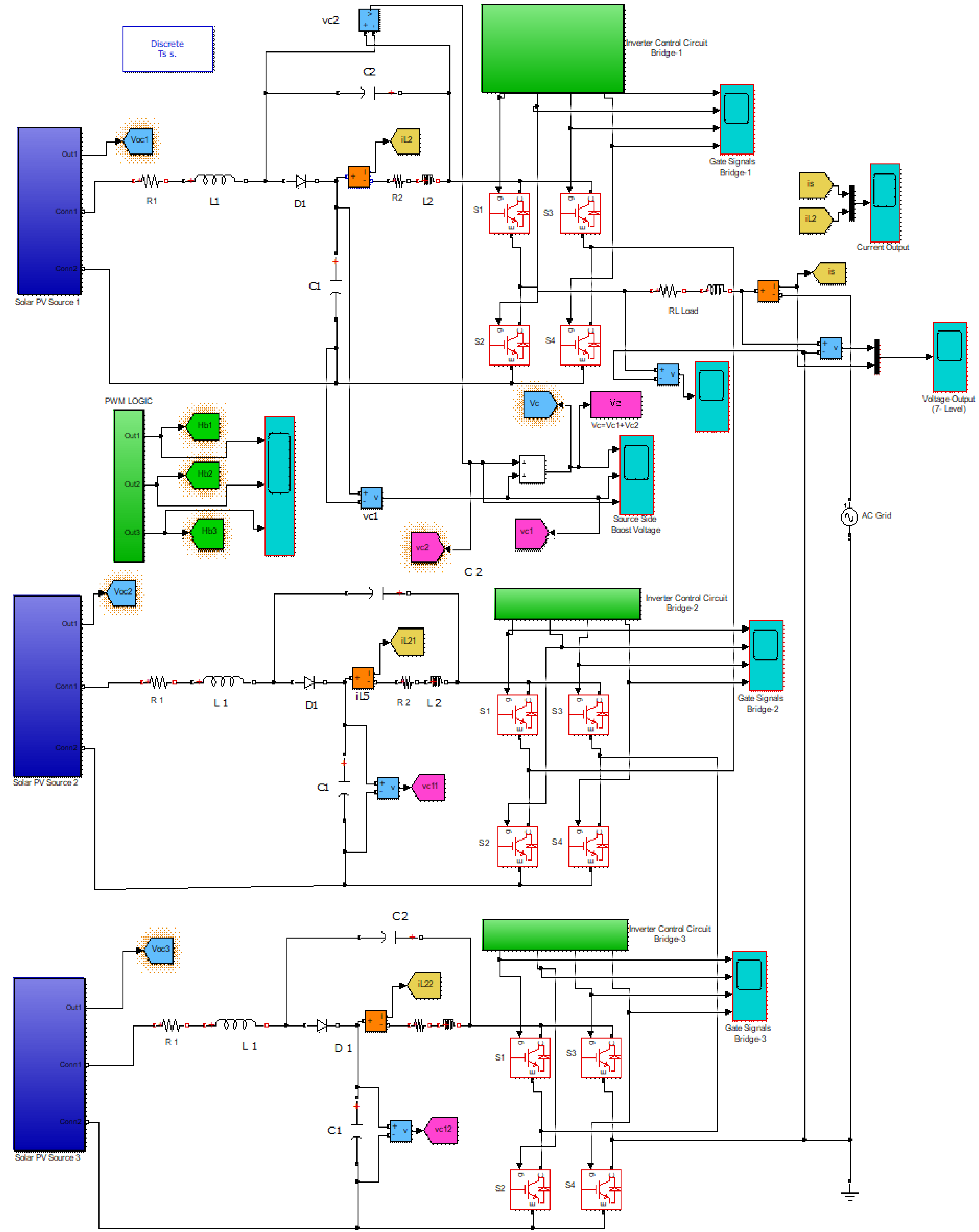
Figure 19 shows the PV sourced five-level cascaded H-bridge qZMLI, in which there are two H-bridge circuits cascaded at the output side and two PV sources used for the supply of each bridge. In both the circuits, inductors at the source side are used to boost the voltage level.
Table 5 presents the different switching states of the cascaded circuit shown in
Figure 19 [
46,
47]. There are mainly three states of switching in PV sourced five-level cascaded H-bridge qZMLI: active, shoot through, and zero. To achieve the favorable results, the “turn on” switching pattern shown in
Table 8 is designed.
5.2. Switching Strategy Used for 7-Level qZSCMLI
MATLAB/Simulink is used to do a detailed investigation of seven levels of qZS-CMLI in this section.
Figure 20 depicts the structure of the seven-level cascaded H-Bridge ZS-MLI.
When compared to the operational states of a typical H-bridge module, the qZSI module adds shoot-through states 1 and 2. As a result, T
s has five operational states: traditional zero states 1 and 2, shoot-through states 1 and 2, and active state [
2].
Figure 21 depicts the corresponding circuit for each operational condition. During one switching cycle, the ON-state currents of the devices in the qZSI module differ, affecting the device’s power loss [
31]. For all devices,
Table 6 summarizes the conduction currents and time intervals. The parameters of qZS-CHBMLI used in MATLAB/Simulink are listed in
Table 7 [
2,
48,
49,
50].
6. Modeling and Performance of a 7-Level Quasi Z-Source Cascaded Multilevel Inverter (qZSCMLI) with Phase Shift (PS) Switching Based on SPV
As per the analysis in this paper, phase shift (PS) switching strategy is the best switching scheme and CHB-MLI the best multilevel inverter topology. Therefore, to avoid the limitation of large voltage change of voltage source inverters (VSI) due to extra DC–DC converters being used at the source side, in the system, a quasi-Z-source inverter is used with the best switching scheme, i.e., PS, and the best MLI topology, i.e., CHB-MLI [
51,
52]. Power inverters, which switch from direct current to alternating current in a single stage include Z-source inverters. Due to its distinctive circuit design, it performs as a buck–boost inverter without using a DC–DC converter bridge. Modifications and new Z-source topologies have increased dramatically in quantity. Recently, it has also been suggested to enhance impedance networks by adding linked magnetism in order to improve voltage even more with a reduced shoot-through time [
53,
54,
55,
56].
The quasi-Z-source cascaded multilevel inverter has increased reliability and wide voltage control through a boost factor and modulation index, and it can perform single-stage power conversion. Reduced THD and dependability against short circuits are additional benefits of the quasi-Z-source modified cascaded multilevel inverter. By combining the multicarrier pulse-width-modulation technique with straightforward boost control, which launches shoot-through states into the conventional zero states to control the quasi-Z-source CMLI module, a multilevel output voltage waveform of the quasi-Z-source CMLI is created. The boost control approach produces output voltage with a large voltage gain by using the maximum modulation index. This study analyzes the phase shift pulse-width-modulation control system on the proposed topology in conjunction with a straightforward boost control [
57,
58,
59,
60,
61].
The suggested multilevel inverter’s general circuit diagram is shown in
Figure 20. If the number of levels rises, add a switch for every additional level in the control circuits. This topology can use special modulation techniques. A very simple formula can be used to determine how many switches are needed for each level. The current flow from point source side to load side will produce a positive polarity, whereas the flow from load side to source side will produce a negative polarity, as illustrated in the accompanying
Figure 21. To obtain a positive half, properly turn on the switches. Generally, the same and equal DC source voltage should be used in order to obtain equivalent voltage steps. The various voltage steps are produced by the uneven V
dc. A new PV system based on a quasi-Z-source CHBMLI is proposed with phase shift switching topology in this paper. Due to some distinct qualities, Z-source inverters and quasi-Z-source inverters are now frequently used for renewable energy power-generating systems. Because shoot-through cases no longer harm the inverter, they can implement voltage boost and power conversion concurrently in a single stage and increase dependability. PV systems are entirely dependent on solar energy, which repeatedly demonstrates their immense ability to function as a pure and limitless renewable energy source. Each PV array and quasi-Z-source capacitors charge the inductors during shoot-through states, and the diode is cut off by the negative voltage.
With fewer switches, a voltage-boost capability that is not restricted to input voltage (DC source) summing, single-stage conversion, and durability against short circuits, the proposed qZS-CHBMLI topology offers appealing benefits. The qZS-CHBMLI performance parameters are examined and displayed using the phase shift PWM control method. Better outcomes are obtained when the phase shift PWM control approach is paired with a straightforward boost control technique. For photovoltaic-based applications, this proposed qZS-CHBMLI topology is more appropriate and effective.
In the simulation circuit, conducting current and conducting time are assumed as per
Table 9, while the parameters’ values used are given in
Table 10 for clarity.
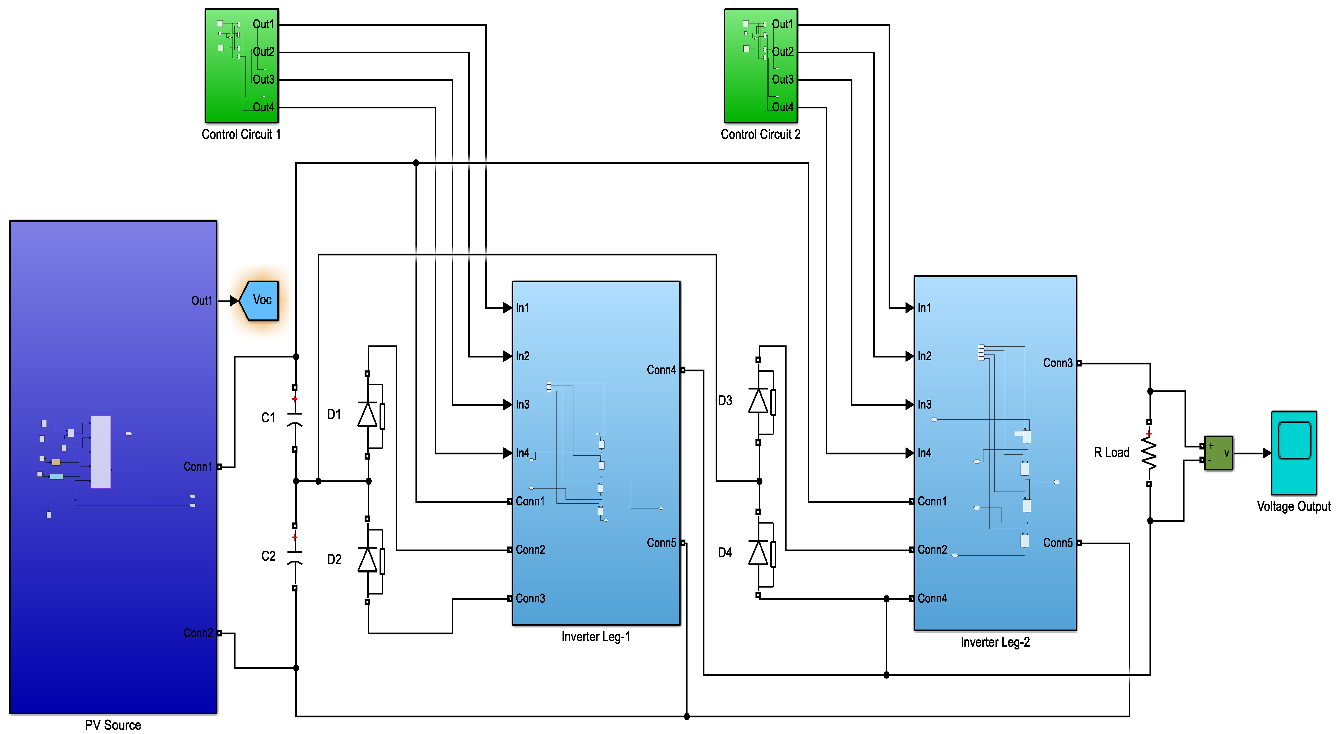
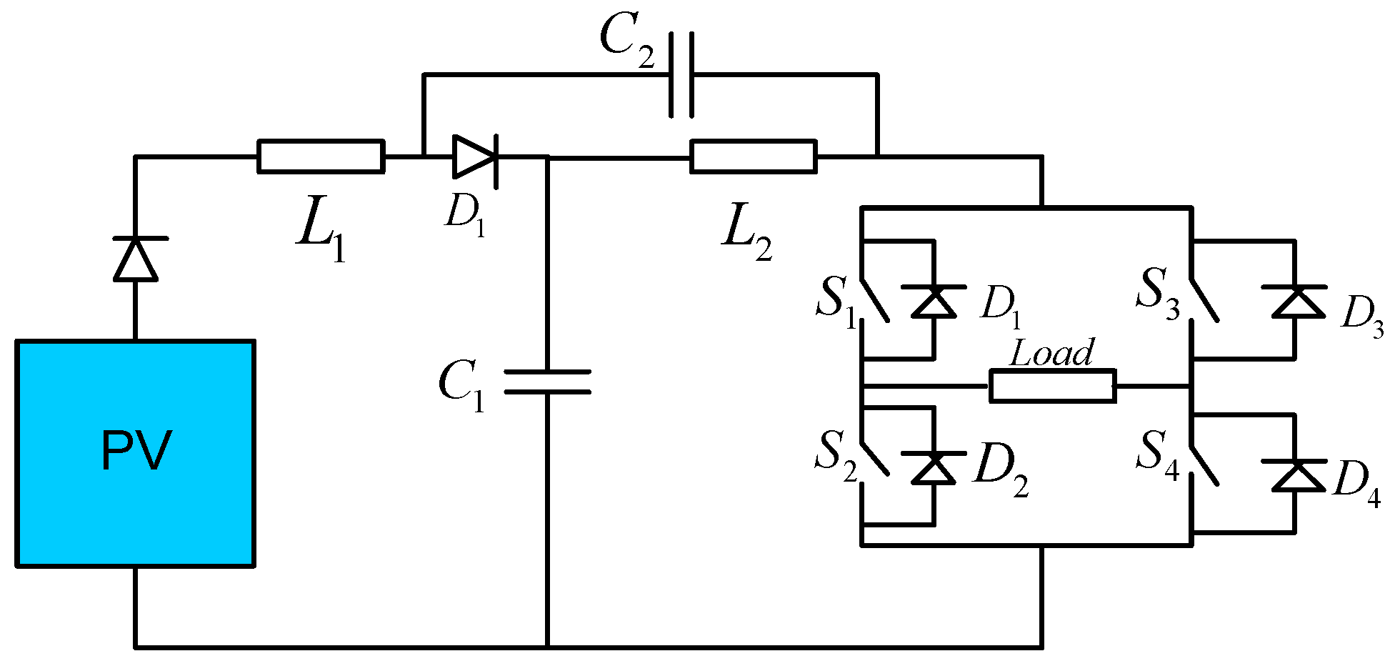
Figure 22 and
Figure 23 depict the standard qZS CHB MLI. It has a qZS network made up of one diode (D
1), two inductors (L
1, L
2), and two capacitors (C
1, C
2). The inverter and qZS network share a common ground and a continuous DC source. This topology is a symmetric cascaded H-bridge inverter topology that has been simplified.
Figure 22 and
Figure 23 show the simulation circuit for the seven-level qZS-CHB-MLI. To incorporate the shoot-through states into the PWM pulses, a simple boost control approach is used.
7. Results and Discussion
Lower-order harmonics, as well as the modified sinusoidal output voltage, can be avoided or reduced using PWM approaches. The need for filters is also minimized. Furthermore, it is seen from the various results that the unipolar phase-shifted technique has more merits in comparison to others for multilevel inverters.
It could be summarized that every topology has its own merits and demerits. When compared to CHB-MLI, just eight switches are required, which is fewer than any other topology. In addition, this topology does not suffer from the major drawback of voltage balancing due to asymmetric capacitors. CHB-MLI requires no unidirectional switches, which is also an advantage. The switching operation is also very simple in CHB-MLI relative to other discussed topologies. The capability of adding separate DC source or photovoltaic (PV) string increases the modularity of CHB-MLI. Thus, CHB-MLI topology is more beneficial and an effective solution for medium voltage requirements along with higher efficiency and modular structure.
From the topological study of multilevel inverters, the cascaded H-bridge MLI has better THD. Because there are fewer switching devices, there is a lower chance of failure. For photovoltaic (PV) applications, cascaded H-bridge MLI is more promising. It necessitates several or two distinct SPV array sources as a voltage supply for each cell of a multilevel inverter, and it is also preferred over other topologies.
The simulation was run with SPV as a source at each H-bridge.
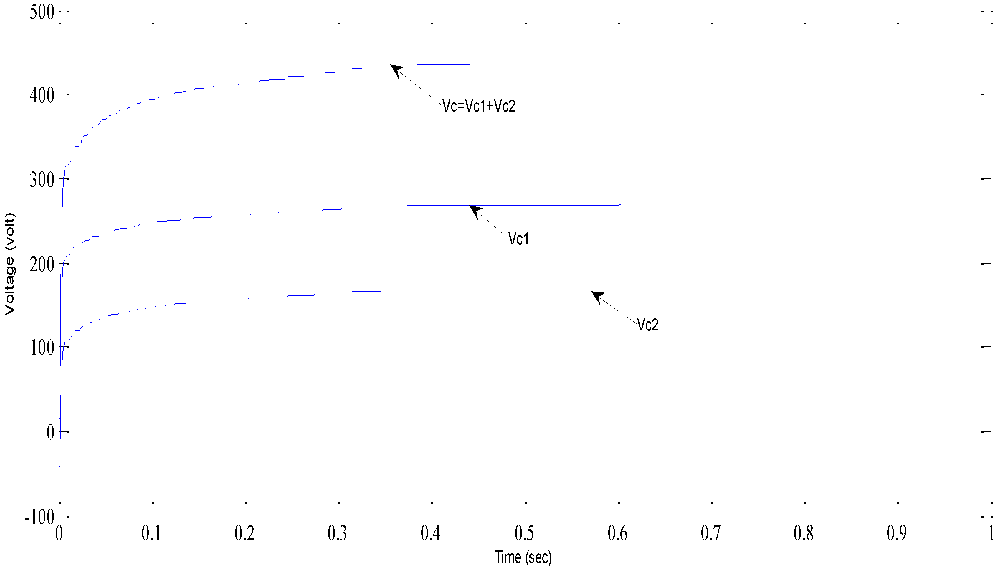
Figure 24 shows the source-side boost voltage across the capacitor of qZS-CHBMLI. The qZS-CHBMLI has a continuous current waveform as shown in
Figure 25 because of the presence of the Z network between the PV source and the H-bridge inverter. Since it works in the shoot-through state, it will not lessen the output voltage.
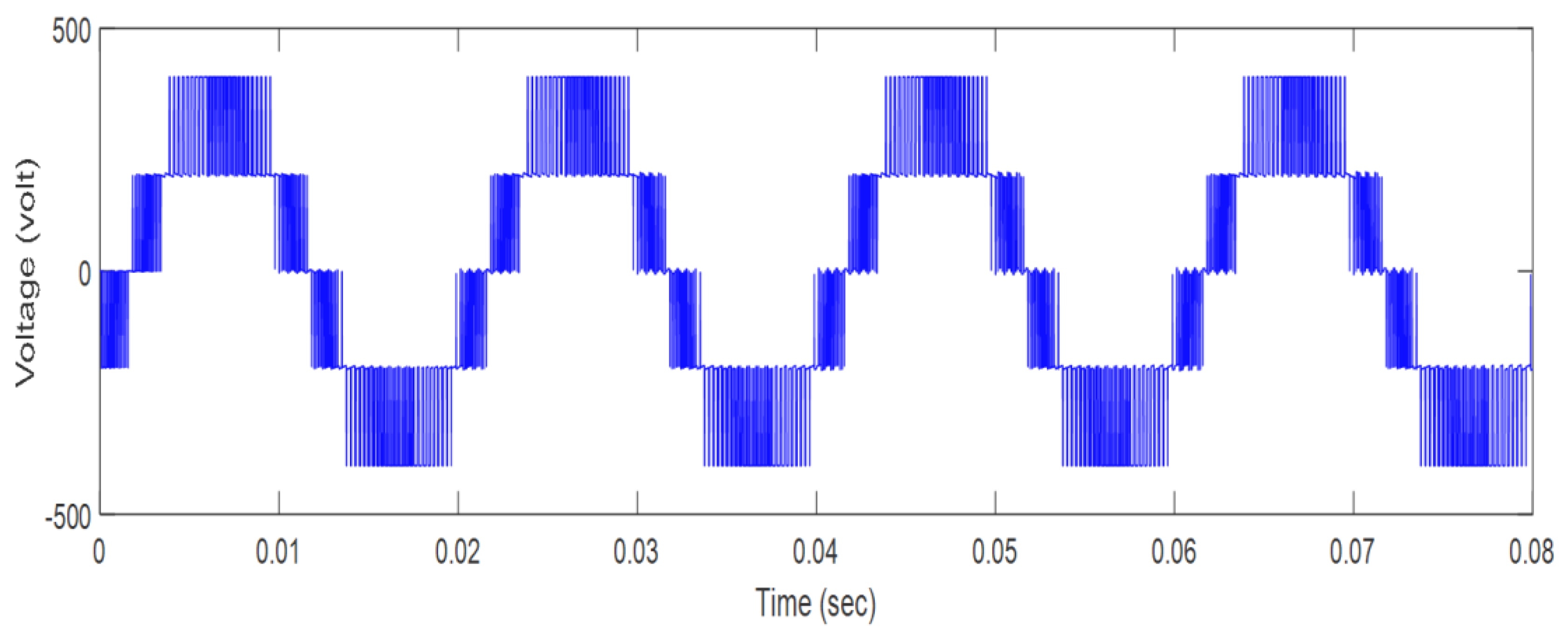
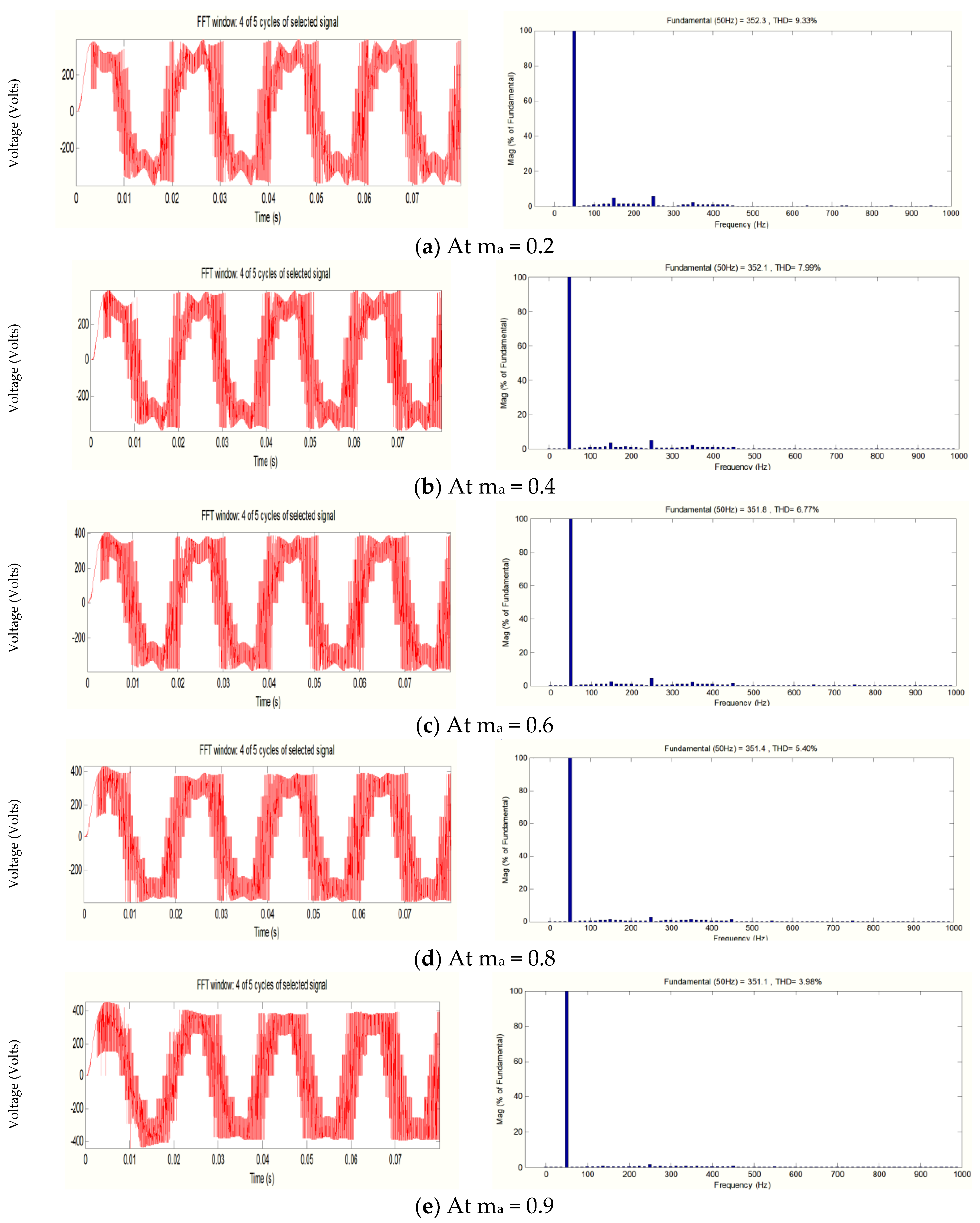
Figure 26 depicts qZS-CHBMLI voltage output with seven levels.
As seen in
Table 11, the effect of the modulation index (m
a) on qZS-CHBMLI voltage output is that the greater modulation index (m
a) value results in less THD. It can also be verified through
Figure 27a–e. As a result, it can be concluded that qZS-CHBMLI can be used effectively in photovoltaic applications.
As such, according to the output obtained from the seven level Simulink model of the qZS-CHBMLI, the electrical power quality improves when the modulation index rises (
Figure 27a–e).
8. Conclusions
The primary contributions of this research paper are as follows.
An analysis of solar photovoltaic based inverters with different switching strategies was conducted, and it was seen from the various results that the unipolar phase-shifted technique has more advantages in comparison to others for multilevel inverters. From the topological study of multilevel inverters, the cascaded H-bridge MLI had better THD. Because there are fewer switching devices, for photovoltaic (PV) applications, the CHB-MLI is more promising.
One more contribution of this scheme is to avoid the major drawback of typical voltage source inverters that cannot handle large voltage changes and an additional DC–DC converter must be used to provide additional voltage boost. This issue can be tackled with Z-source inverters. The quasi-Z-source inverter (qZSI) adds a number of special features, including the ability to pull a steady current from the input source and lessen the capacitor voltage rating. As a result, the qZS-CMI is more adapted for power generation using strings of solar PV source.
Author Contributions
A.A.K., R.K.P. and F.P.G.M.; Data curation, A.F.M., R.K.P. and A.A.J.; Formal analysis, A.F.M. and R.K.P.; Funding acquisition, A.A.K., H.M. and F.P.G.M.; Investigation, A.F.M., A.A.K., R.K.P., H.M. and A.A.J.; Methodology, A.F.M. and R.K.P.; Project administration, H.M. and F.P.G.M.; Resources, A.A.J.; Software, H.M. and A.A.J.; Supervision, F.P.G.M.; Validation, F.P.G.M.; Visualization, A.F.M. and F.P.G.M.; Writing—original draft, A.A.K.; Writing—review & editing, H.M. and F.P.G.M. All authors have read and agreed to the published version of the manuscript.
Funding
The work reported here in has been financially supported by the Spanish Ministerio de Ciencia e Innovación and the European Regional Development Fund under Research Grant RTC2019-007364-3.
Institutional Review Board Statement
Not applicable.
Informed Consent Statement
Not applicable.
Data Availability Statement
Not applicable.
Acknowledgments
The authors would like to acknowledge the support from Ingenium Research Group, Universidad Castilla-La Mancha, 13071 Ciudad Real, Spain, support from Integral University, Lucknow, support from Universiti Teknologi Malaysia (UTM), and support from Intelligent Prognostic Private Limited Delhi, India researcher’s supporting Project.
Conflicts of Interest
The authors declare no conflict of interest.
References
- Kouro, S.; Angulo, M.; Rodriguez, J.; Pontt, J. Multicarrier PWM with DC-Link Ripple Feed forward for Multilevel Inverters. In Proceedings of the 12th International Power Electronics and Motion Control Conference, Portoroz, Slovenia, 30 August–1 September 2006. [Google Scholar]
- Sun, D.; Ge, B.; Yan, X.; Bi, D.; Zhang, H.; Liu, Y.; Abu-Rub, H.; Brahim, L.B.; Peng, F.Z. Modeling, Impedance Design, and Efficiency Analysis of Quasi-Z Source Module in Cascaded Multilevel Photovoltaic Power System. IEEE Trans. Ind. Electron. 2014, 61, 6108–6117. [Google Scholar] [CrossRef]
- Ge, B.; Abu-Rub, H.; Peng, F.Z.; Lei, Q.; de Almeida, A.; Ferreira, F.; Sun, D.; Liu, Y. An energy stored quasi-Z-source inverter for application to photovoltaic power system. IEEE Trans. Ind. Electron. 2013, 60, 4468–4481. [Google Scholar] [CrossRef]
- Minai, A.F.; Usmani, T.; Iqbal, A.; Mallick, M.A. Artificial Bee Colony Based Solar PV System with Z-Source Multilevel Inverter. In Proceedings of the 2020 IEEE International Conference on Advances in Computing, Communication & Materials (ICACCM), Dehradun, India, 21–22 August 2020; pp. 187–193. [Google Scholar] [CrossRef]
- Rashid, M.H. Power Electronics Circuits, Devices and Applications; Prentice Hall of India: New Delhi, India, 2004. [Google Scholar]
- Rahman, S.; Meraj, M.; Iqbal, A.; Prathap-Reddy, B.; Khan, I. A Combinational Level Shifted and Phase Shifted PWM Technique for Symmetrical Power Distribution in CHB Inverters. IEEE J. Emerg. Sel. Top. Power Electron. 2021, 9509488. [Google Scholar] [CrossRef]
- Navyanagath, C.G.; Purnima, S.V.; Veerakumar, S. Comparison of PWM Methods for Multilevel Inverter. Int. J. Adv. Res. Electr. 2013, 2, 6106–6114. [Google Scholar]
- Zhong, D. Active Harmonic Elimination in Multilevel Converters. Ph.D. Thesis, The University of Tennessee, Knoxville, TN, USA, 2005. [Google Scholar]
- Asghar, M.S.J. Power Electronics; Prentice-Hall of India Private Limited: New Delhi, India, 2004. [Google Scholar]
- Minai, A.F.; Usmani, T.; Mallick, M.A. Performance analysis of Multilevel inverter with SPWM strategy using MATLAB/SIMULINK. J. Electr. Eng. JEE 2016, 16, 428–433. [Google Scholar]
- Lai, J.S.; Peng, F.Z. Multilevel Converters—A New Breed of Power Converters. IEEE Trans. Ind. Appl. 1996, 32, 509–517. [Google Scholar]
- Minai, A.F.; Tariq, A. Analysis of Cascaded Multilevel Inverter. In Proceedings of the India International Conference on Power Electronics 2010 (IICPE2010), New Delhi, India, 28–30 January 2011; pp. 1–6. [Google Scholar]
- Manjrekar, M.D.; Steimer, P.K.; Lipo, T.A. Hybrid multilevel power Conversion system: A competitive solution for high-power applications. IEEE Trans. Ind. Appl. 2000, 36, 834–841. [Google Scholar] [CrossRef]
- Wheeler, P.W.; Empringham, L. Improved Output Waveform Quality for Multilevel H Bridge Chain Converters Using Unequal Cell Voltages. In Proceedings of the IEEE Power Electronics and Variable Speed Drives Conference, London, UK, 18–19 September 2000; pp. 536–540. [Google Scholar]
- Matnani, M.K. Design and Implementation of DSP based Control of Hybrid Cascaded Multilevel Inverter Using various Novel Pulse Width Modulation Techniques. Ph.D. Thesis, the Maharaja Sayajirao University of Baroda, Gujrat, India, February 2014. [Google Scholar]
- Mussa, S.A. New symmetrical hybrid multilevel DC-AC converters. In Proceedings of the IEEE Power Electronics Specialists Conference, Rhodes, Greece, 15–19 June 2008. [Google Scholar]
- Chen, A.; He, X. Research on hybrid-clamped multilevel inverter topologies. IEEE Trans. Ind. Electron. 2006, 53, 1898–1907. [Google Scholar] [CrossRef]
- Zhao, J. A novel PWM control method to eliminate the effect of dead time on the output waveform for hybrid clamped multilevel inverters. In Proceedings of the 25th Annual IEEE Applied Power Electronics Conference and Exposition (APEC), Palm Springs, CA, USA, 21–25 February 2010. [Google Scholar]
- Bhagwat, P.M.; Stefanovic, V.R. Generalized Structure of a Multilevel PWM Inverter. IEEE Trans. Ind. Appl. 1983, 19, 1057–1069. [Google Scholar] [CrossRef]
- Ahmad, S.; Iqbal, A.; Ali, M.; Rahman, K.; Ahmed, A.S. A Fast Convergent Homotopy Perturbation Method for Solving Selective Harmonics Elimination PWM Problem in Multi Level Inverter. IEEE Access 2021, 9, 113040–113051. [Google Scholar] [CrossRef]
- Rech, C.; Pinheiro, J.R. Hybrid Multilevel Converters: Unified Analysis and Design Considerations. IEEE Trans. Ind. Electron. 2007, 54, 1092–1104. [Google Scholar] [CrossRef]
- Rech, C.; Pinheiro, J.R. Impact of Hybrid Multilevel Modulation Strategies on Input and Output Harmonic Performances. IEEE Trans. Power Electron. 2007, 22, 967–977. [Google Scholar] [CrossRef]
- Ozdemir, E.; Ozdemir, S.; Tolbert, L.M. Fundamental-Frequency-Modulated Six-Level Diode-Clamped Multilevel Inverter for Three-Phase Stand-Alone Photovoltaic System. IEEE Trans. Ind. Electron. 2009, 56, 4407–4415. [Google Scholar] [CrossRef]
- Kouro, S.; Malinowski, M.; Gopakumar, K.; Pou, J.; Franquelo, L.G.; Wu, B.; Rodriguez, J.; Pérez, M.A.; Leon, J.I. Recent Advances and Industrial Applications of Multilevel Converters. IEEE Trans. Ind. Electron. 2010, 57, 2553–2580. [Google Scholar] [CrossRef]
- Ounejjar, Y.; Hadded, K.A.; Gregoire, L.A. Packed U cells multilevel converter topology: Theoretical study and experimental validation. IEEE Trans. Ind. Electron. 2011, 58, 1294–1306. [Google Scholar] [CrossRef]
- Liao, Y.H.; Lai, C.M. Letters-Newly-Constructed Simplified Single-Phase Multi-string Multilevel Inverter Topology for Distributed Energy Resources. IEEE Trans. Power Electron. 2011, 26, 2386–2392. [Google Scholar] [CrossRef]
- Ounejjar, Y.; Hadded, K.A.; Dessaint, L.A. A novel six band hysteresis control for packed U cell seven level converter: Experimental validation. IEEE Trans. Ind. Electron. 2012, 59, 3808–3816. [Google Scholar] [CrossRef]
- Zhang, X.; Spencer, J.W. Study of Multisampled Multilevel Inverters to Improve Control Performance. IEEE Trans. Power Electron. 2012, 27, 4409–4416. [Google Scholar] [CrossRef]
- Kangarlu, M.F.; Babaei, E. A Generalized Cascaded Multilevel Inverter Using Series Connection of Sub-multilevel Inverters. IEEE Trans. Power Electron. 2013, 28, 625–636. [Google Scholar] [CrossRef]
- Liu, Y.; Ge, B.; Abu-Rub, H.; Peng, F.Z. Control system design of battery-assisted quasi-Z-source inverter for grid-tie photovoltaic power generation. IEEE Trans. Sustain. Energy 2013, 4, 994–1001. [Google Scholar] [CrossRef]
- Liu, Y.; Ge, B.; Abu-Rub, H.; Peng, F.Z. An effective control method for quasi-Z-source cascade multilevel inverter-based grid-tie single-phase photovoltaic power system. IEEE Trans. Ind. Inf. 2014, 10, 399–407. [Google Scholar] [CrossRef]
- Peddapelli, S.K. Recent Advances in Pulse Width Modulation Techniques and Multilevel Inverters. World Acad. Sci. Eng. Technol. Int. J. Electr. Comput. Electron. Commun. Eng. 2014, 8, 570–578. [Google Scholar]
- Babaei, E.; Alilu, S.; Laali, S. A New General Topology for Cascaded Multilevel Inverters with Reduced Number of Components Based on Developed H-Bridge. IEEE Trans. Ind. Electron. 2014, 61, 3932–3939. [Google Scholar] [CrossRef]
- Ruderman, A. About Voltage Total Harmonic Distortion for Single- and Three-Phase Multilevel Inverters. IEEE Trans. Ind. Electron. 2015, 62, 1548–1551. [Google Scholar] [CrossRef]
- Anand, R.; Kamatchi, M. A Fifteen Level Cascaded H-Bridge Multilevel Inverter with Reduced Number of Switches. Int. J. Adv. Eng. Res. Sci. IJAERS 2015, 2, 17–25. [Google Scholar]
- Nithin, R.; Jagadanand, G.; Saly, G. A Modified Charge Balancing Scheme for Cascaded H-Bridge Multilevel Inverter. J. Power Electron. 2016, 16, 2067–2075. [Google Scholar] [CrossRef]
- Durga Prasad, G.; Jegasethan, V.; Rao, P.V.V.R. Hybrid multilevel DC link inverter with reduced power electronic switches. Energy Procedia 2017, 117, 626–634. [Google Scholar] [CrossRef]
- Reddy, S.R.; Prasad, P.V.; Srinivas, G.N. Simulation and Comparison of Twenty Five Level Diode Clamped & Cascaded H-Bridge Multilevel Inverter. Iran. J. Electr. Electron. Eng. 2018, 14, 95–105. [Google Scholar] [CrossRef]
- Mali, R.; Adam, N.; Vaidya, A.S.A.P. Performance Comparison of Two Level Inverter with Classical Multilevel Inverter Topologies. In Proceedings of the 2019 IEEE International Conference on Electrical, Computer and Communication Technologies (ICECCT), Coimbatore, India, 20–22 February 2019; pp. 1–7. [Google Scholar] [CrossRef]
- Yuditya, B.H.; Hasanah, R.N.; Ardhenta, L.; Taufik, T. Performance Comparison of Single-Phase Multilevel Inverter with SPWM Unipolar and Bipolar Switching Techniques. In Proceedings of the 2020 FORTEI-International Conference on Electrical Engineering (FORTEI-ICEE), Bandung, Indonesia, 23–24 September 2020. [Google Scholar] [CrossRef]
- Agrawal, N.; Goswami, S.; Bagaria, R.; Muthele, A. A Comparative Brief Study on Level-Shifted Pulse Width Modulation and Hybrid Pulse Width Modulation Switching Techniques for 7-Level CHB Single-Phase Inverter. In Advances in Smart Grid and Renewable Energy; ETAEERE 2020. Lecture Notes in Electrical Engineering; Sherpa, K.S., Bhoi, A.K., Kalam, A., Mishra, M.K., Eds.; Springer: Singapore, 2021; Volume 691. [Google Scholar] [CrossRef]
- Fahad, M.; Tariq, M.; Faizan, M.; Ali, A.; Sarwar, A.; Dehghani Tafti, H.; Ahmad, S.; Shah Noor Mohamed, A. A Dual Source Switched-Capacitor Multilevel Inverter with Reduced Device Count. Electronics 2022, 11, 67. [Google Scholar] [CrossRef]
- Ghazanfari, A.; Mokhtari, H.; Firouzi, M. Simple Voltage Balancing Approach for CHB Multilevel Inverter Considering Low Harmonic Content Based on a Hybrid Optimal Modulation Strategy. IEEE Trans. Power Deliv. 2012, 27, 2150–2158. [Google Scholar] [CrossRef]
- Peng, F.Z. Z-Source Inverter. IEEE Trans. Ind. Appl. 2003, 39, 504–510. [Google Scholar] [CrossRef]
- Vinnikov, D.; Roasto, I.; Strzelecki, R.; Adamowicz, M. Step-up DC/DC converters with cascaded quasi-Z-source network. IEEE Trans. Ind. Electron. 2012, 59, 3727–3736. [Google Scholar] [CrossRef]
- Liu, L.; Li, H.; Zhao, Y.; He, X.; Shen, Z.J. 1 MHz cascaded Z source inverters for scalable grid-interactive photovoltaic (PV) applications using GaN device. In Proceedings of the 2011 IEEE Energy Conversion Congress and Exposition, Phoenix, AZ, USA, 17–22 September 2011; pp. 2738–2745. [Google Scholar]
- Liu, Y.; Ge, B.; Abu-Rub, H.; Peng, F.Z. Overview of space vector modulations for three-phase Z-source/quasi-Z-source inverters. IEEE Trans. Power Electron. 2014, 29, 2098–2108. [Google Scholar] [CrossRef]
- Meraj, M.; Rahman, S.; Iqbal, A.; Ben-Brahim, L.; Abu-Rub, H.A. Novel Level-Shifted PWM Technique for Equal Power Sharing Among Quasi-Z-Source Modules in Cascaded Multilevel Inverter. IEEE Trans. Power Electron. 2021, 36, 4766–4777. [Google Scholar] [CrossRef]
- Meraj, M.; Rahman, S.; Iqbal, A.; Ben-Brahim, L. Common mode voltage reduction in a singlephase quasi Z-source inverter for transformerless grid-connected solar PV applications. IEEE J. Emerg. Sel. Top. Power Electron. 2019, 7, 1352–1363. [Google Scholar] [CrossRef]
- Abduallah, A.A.; Iqbal, A.; Meraj, M.; Ben-Brahim, L.; Alammari, R.; Abu-Rub, H. Discontinuous space vector pulse width modulation techniques for a five-phase quasi Z-source inverter. In Proceedings of the 41st Annual Conferenece IEEE Industrial Electronics Society, Yokohama, Japan, 9–12 November 2015; pp. 4205–4210. [Google Scholar]
- Rahman, S.; Meraj, M.; Iqbal, A.; Tariq, M.; Maswood, A.I.; Ben-Brahim, L.; Alammari, R. Cascaded multilevel qZSI powered single-phase induction motor for water pump application. In Proceedings of the 2017 IEEE Energy Conversion Congress and Exposition (ECCE), Cincinnati, OH, USA, 1–5 October 2017; pp. 1037–1042. [Google Scholar] [CrossRef]
- Mahmood, A.; Zaid, M.; Khan, S.; Siddique, M.D.; Iqbal, A.; Sarwer, Z. A non-isolated quasi-Z-source-based high-gain DC–DC converter. Int. J. Circ. Theor. Appl. 2022, 50, 653–682. [Google Scholar] [CrossRef]
- Siddique, M.D.; Iqbal, A.; Sarwar, A.; Mekhilef, S. Analysis and implementation of a new asymmetric double H-bridge multilevel inverter. Int. J. Circ. Theor. Appl. 2021, 49, 4012–4026. [Google Scholar] [CrossRef]
- Erol, C. A new multi-level inverter with reverse connected dual dc to dc converter at simulation. Int. J. Model. Simul. 2022, 42, 34–46. [Google Scholar] [CrossRef]
- Erol, C. The inverter with reverse connected double converter driving unbalanced loads. Int. J. Model. Simul. 2022, 42, 217–226. [Google Scholar] [CrossRef]
- Tomar, A.; Malik, H.; Kumar, P.; Iqbal, A. Machine Learning, Advances in Computing, Renewable Energy and Communication. In Machine Learning, Advances in Computing, Renewable Energy and Communication, 1st ed.; Springer: Singapore, 2022; Volume 781, p. XV. ISBN 978-981-19-2828-4. [Google Scholar]
- Puthiyapurayil, M.R.M.K.; Nasirudeen, M.N.; Saywan, Y.A.; Ahmad, W.; Malik, H. A Review of Open-Circuit Switch Fault Diagnostic Methods for Neutral Point Clamped Inverter. Electronics 2022, 11, 3169. [Google Scholar] [CrossRef]
- Can, E. The load performance of multi-level alternating voltage provided by upgrade effect. J. Kejuruter. 2019, 31, 249–259. [Google Scholar] [CrossRef]
- Erol, C.; Hasan, H.S. Development of fractional sinus pulse width modulation with β gap on three step signal processing. Int. J. Electron. 2022, 1–20. [Google Scholar] [CrossRef]
- Erol, C. The levels effect of the voltage generated by an inverter with partial source on distortion. Int. J. Electron. 2020, 107, 1414–1435. [Google Scholar] [CrossRef]
- Ahmad, W.; Gorla, N.B.Y.; Malik, H.; Panda, S.K. Noninvasive Model-Based Open-Circuit Switch Fault Detection of AC-Bypass Leg Switches in Transformerless PV Inverter. IEEE J. Emerg. Sel. Top. Power Electron. 2021, 9, 6671–6680. [Google Scholar] [CrossRef]
Figure 1.
Classification of modulation strategies.
Figure 1.
Classification of modulation strategies.
Figure 2.
Carrier arrangements of (a) phase disposition (PD); (b) phase opposition disposition (POD); (c) alternative phase opposition disposition (APOD); and (d) phase shifted (PS) techniques.
Figure 2.
Carrier arrangements of (a) phase disposition (PD); (b) phase opposition disposition (POD); (c) alternative phase opposition disposition (APOD); and (d) phase shifted (PS) techniques.
Figure 3.
(a) Total harmonic distortion; (b) total harmonic distortion (THD) using unipolar technique (THD) using bipolar technique.
Figure 3.
(a) Total harmonic distortion; (b) total harmonic distortion (THD) using unipolar technique (THD) using bipolar technique.
Figure 4.
THD of the output voltage for varied ma at different switching approaches.
Figure 4.
THD of the output voltage for varied ma at different switching approaches.
Figure 5.
Circuit topologies for 5-leveldiode-clamped multilevel inverters.
Figure 5.
Circuit topologies for 5-leveldiode-clamped multilevel inverters.
Figure 6.
Five-level FC-MLI.
Figure 6.
Five-level FC-MLI.
Figure 7.
Topology of a 5-level CHB-MLI.
Figure 7.
Topology of a 5-level CHB-MLI.
Figure 8.
Five-level asymmetric hybrid MLI.
Figure 8.
Five-level asymmetric hybrid MLI.
Figure 9.
New 5-level symmetrical hybrid multilevel inverter.
Figure 9.
New 5-level symmetrical hybrid multilevel inverter.
Figure 10.
HC 5-level inverter.
Figure 10.
HC 5-level inverter.
Figure 11.
Simulation of a 2-leg, 5-level DC-MLI.
Figure 11.
Simulation of a 2-leg, 5-level DC-MLI.
Figure 12.
Five-level DC-MLI output voltage waveform.
Figure 12.
Five-level DC-MLI output voltage waveform.
Figure 13.
Simulation of a five-level FC-MLI.
Figure 13.
Simulation of a five-level FC-MLI.
Figure 14.
A five-level FC-MLI Simulink model’s voltage output.
Figure 14.
A five-level FC-MLI Simulink model’s voltage output.
Figure 15.
Cascaded 5-level CHB-MLI simulation model.
Figure 15.
Cascaded 5-level CHB-MLI simulation model.
Figure 16.
Five-level CHB-MLI output voltage waveform.
Figure 16.
Five-level CHB-MLI output voltage waveform.
Figure 17.
qZSMLI with PV power generation system.
Figure 17.
qZSMLI with PV power generation system.
Figure 18.
qZSI’s equivalent circuit.
Figure 18.
qZSI’s equivalent circuit.
Figure 19.
Five level qZSMLI with PV source.
Figure 19.
Five level qZSMLI with PV source.
Figure 20.
Seven-level qZSMLI with PV source.
Figure 20.
Seven-level qZSMLI with PV source.
Figure 21.
Equivalent circuits in one switching cycle.
Figure 21.
Equivalent circuits in one switching cycle.
Figure 22.
An H-bridge PV-powered qZS CMLI modeled in Simulink.
Figure 22.
An H-bridge PV-powered qZS CMLI modeled in Simulink.
Figure 23.
A complete H-bridge PV-powered qZS-CMLI modeled in Simulink.
Figure 23.
A complete H-bridge PV-powered qZS-CMLI modeled in Simulink.
Figure 24.
Source-side boost voltage across the capacitor of qZS-CHBMLI.
Figure 24.
Source-side boost voltage across the capacitor of qZS-CHBMLI.
Figure 25.
Current output of qZS-CHBMLI.
Figure 25.
Current output of qZS-CHBMLI.
Figure 26.
qZS-CHBMLI voltage output with seven levels.
Figure 26.
qZS-CHBMLI voltage output with seven levels.
Figure 27.
qZS-CHBMLI THD analysis.
Figure 27.
qZS-CHBMLI THD analysis.
Table 1.
Switching of the inverter.
Table 1.
Switching of the inverter.
| S. No. | Switching Signal | Switching States * |
|---|
| 1 | 000 | 0 |
| 2 | 001 | 1 |
| 3 | 010 | 1 |
| 4 | 011 | 1 |
| 5 | 100 | 1 |
| 6 | 101 | 1 |
| 7 | 110 | 1 |
| 8 | 111 | 0 |
Table 2.
Comparison of components required for various topologies.
Table 2.
Comparison of components required for various topologies.
| Inverter Configuration | DC-
MLI | FC-
MLI | CHB-
MLI | AH-
MLI | NSH-
MLI | HC-
MLI |
|---|
| Main switching devices | 8 | 8 | 8 | 8 | 8 | 14 |
| Clamping diodes | 12 | 0 | 0 | 8 | 8 | 6 |
| Balancing capacitors | 0 | 12 | 0 | 0 | 0 | 3 |
| DC bus capacitors | 4 | 4 | 0 | 2 | 2 | 4 |
| Main diodes | 8 | 8 | 0 | 0 | 0 | 6 |
Table 3.
Methods for inverter level comparisons.
Table 3.
Methods for inverter level comparisons.
| S. No. | References | Levels | Switches | THD (%) |
|---|
| 1 | [19] | 3 | 8 | 16.86 |
| 2 | [11] | 5 | 8 | 7.19 |
| 3 | [20] | 3 | 4 | 15 |
| 4 | [21] | 9 | 8 | 16.3 |
| 5 | [22] | 11 | 12 | 12.8 |
| 6 | [23] | 9 | 8 | 10.4 |
| 7 | [24] | 6 | 10 | 6.3 |
| 8 | [25] | 7 | 6 | 24.32 |
| 9 | [26] | 5 | 6 | 3 |
| 10 | [27] | 7 | 6 | 22 |
| 11 | [28] | 5 | 8 | 2.3 |
| 12 | [29] | 13 | 14 | 1.44 |
| 13 | [30] | 9 | 12 | 19.7 |
| 14 | [31] | 13 | 18 | 14.1 |
| 15 | [32] | 5 | 8 | 0.64 |
| 16 | [33] | 31 | 10 | 0.94 |
| 17 | [34] | 10 | 18 | 4.8 |
| 18 | [35] | 15 | 8 | 1.65 |
| 19 | [36] | 5 | 8 | 3.33 |
| 20 | [37] | 15 | 11 | 4.01 |
| 21 | [38] | 25 | 48 | 2.81 |
| 22 | [39] | 5 | 8 | 6.02 |
| 23 | [40] | 5 | 8 | 19.9 |
| 24 | [41] | 7 | 6 | 3.03 |
| 25 | [42] | 19 | 10 | 4.3 |
Table 4.
A five-level NPC-switching MLI’s states and output voltage.
Table 4.
A five-level NPC-switching MLI’s states and output voltage.
| State Transition | Voltage
Vo |
|---|
| S1 | S2 | S3 | S4 | S1′ | S2′ | S3′ | S4′ |
|---|
| 1 | 1 | 1 | 1 | 0 | 0 | 0 | 0 | 4E |
| 0 | 1 | 1 | 1 | 1 | 0 | 0 | 0 | 3E |
| 0 | 0 | 1 | 1 | 1 | 1 | 0 | 0 | 2E |
| 0 | 0 | 0 | 1 | 1 | 1 | 1 | 0 | E |
| 0 | 0 | 0 | 0 | 1 | 1 | 1 | 1 | 0 |
Table 5.
Switching diagram of an FC five-level Sinusoidal PWM-MLI.
Table 5.
Switching diagram of an FC five-level Sinusoidal PWM-MLI.
| Switching States | Voltage
Vo |
|---|
| S1 | S2 | S3 | S4 |
|---|
| 1 | 1 | 1 | 1 | 4E |
| 1 | 1 | 1 | 0 | 3E |
| 0 | 1 | 1 | 1 |
| 1 | 0 | 1 | 1 |
| 1 | 1 | 0 | 1 |
| 1 | 1 | 0 | 0 | 2E |
| 0 | 0 | 1 | 1 |
| 1 | 0 | 0 | 1 |
| 0 | 1 | 1 | 0 |
| 1 | 0 | 1 | 0 |
| 0 | 1 | 0 | 1 |
| 1 | 0 | 0 | 0 | E |
| 0 | 1 | 0 | 0 |
| 0 | 0 | 1 | 0 |
| 0 | 0 | 0 | 1 |
| 0 | 0 | 0 | 0 | 0 |
Table 6.
Switching pattern of the switches used in CHB-MLI.
Table 6.
Switching pattern of the switches used in CHB-MLI.
| Switching States | V1 | V2 | Voltage
Vo |
|---|
| S11 | S31 | S12 | S32 |
|---|
| 1 | 0 | 1 | 0 | V | V | 2V |
| 1 | 0 | 1 | 1 | V | 0 | V |
| 1 | 0 | 0 | 0 | V | 0 |
| 1 | 1 | 1 | 0 | 0 | V |
| 0 | 0 | 1 | 0 | 0 | V |
| 0 | 0 | 0 | 0 | 0 | 0 | 0 |
| 0 | 0 | 1 | 1 | 0 | 0 |
| 1 | 1 | 1 | 1 | 0 | 0 |
| 1 | 1 | 0 | 0 | 0 | 0 |
| 1 | 0 | 0 | 1 | V | −V |
| 0 | 1 | 1 | 0 | −V | V |
| 0 | 1 | 1 | 1 | −V | 0 | −V |
| 0 | 1 | 0 | 0 | −V | 0 |
| 1 | 1 | 0 | 1 | 0 | −V |
| 0 | 0 | 0 | 1 | 0 | −V |
| 0 | 1 | 0 | 1 | −V | −V | −2V |
Table 7.
Different inverters’ THDs compared.
Table 7.
Different inverters’ THDs compared.
Modulation Index
(ma) | %THD |
|---|
| 5-Level DC-MLI | Five-Level FC-MLI | Five-Level CHB-MLI |
|---|
| 0.8 | 30.56 | 25.64 | 16.71 |
Table 8.
Five-level qZMLI switching states.
Table 8.
Five-level qZMLI switching states.
| Vo | Switch “Turn on” | State |
|---|
| 2VS | S1,S2,S5,S6 | Active |
| VS | S1, S3,S5,S6 | Active |
| VS | S1,S2,S3,S4,S5,S6 | Shoot-through |
| VS | S1,S2,S5,S7 | Active |
| VS | S1,S2,S5,S6,S7,S8 | Shoot-through |
| 0 | S1,S3,S5,S7 | Zero |
| 0 | S1,S2,S3,S4,S5,S7 | Shoot-through |
| 0 | S1,S3,S5,S6,S7,S8 | Shoot-through |
| −VS | S1,S3,S7,S8 | Active |
| −VS | S1,S2,S3,S4,S7,S8 | Shoot-through |
| −VS | S3,S4,S5,S7 | Active |
| −VS | S3,S4,S5,S6,S7,S8 | Shoot-through |
| −2VS | S3,S4,S7,S8 | Active |
Table 9.
Devices, conducting currents, and conducting time durations of the qZSI module in one switching cycle for the positive half fundamental cycle.
Table 9.
Devices, conducting currents, and conducting time durations of the qZSI module in one switching cycle for the positive half fundamental cycle.
| Devices | Conducting Current | Conducting Time |
|---|
| S1, S4 | ia | TS.(1+m)/2 |
| 2iL1 | TS.D/2 |
| S2, S3 | 2iL1 | TS.D/2 |
| D2, D3 | ia | TS.[1–(1+m)/2] |
| D | 2iL1 | TS.(1–D–m) |
| 2iL1–ia | TS.m |
| L1, L2 | iL1 | TS |
| C1, C2 | −iL1 | TS.D |
| iL1 | TS.(1–D–m) |
| iL1–ia | TS.m |
Table 10.
Simulation parameters of qZMLI.
Table 10.
Simulation parameters of qZMLI.
| qZSI Parameters | Parameters |
|---|
| Capacitors (C1 and C2) | 2000 μF |
| Inductors (L1 and L2) | 400 μH |
| Modulation index (ma) | 0.8 |
| Duty-to-shoot ratio (D) | 0.25 |
| RL Load | 8 Ω and 1 mH |
| Switching frequency “fs” | 10 kHz |
Table 11.
THD analysis of qZS-CHBMLI at different value of ma.
Table 11.
THD analysis of qZS-CHBMLI at different value of ma.
| S.No. | Modulation Index (ma) | % THD |
|---|
| 1. | 0.2 | 9.33 |
| 2. | 0.4 | 7.99 |
| 3. | 0.6 | 6.77 |
| 4. | 0.8 | 5.40 |
| 5. | 0.9 | 3.98 |
| Publisher’s Note: MDPI stays neutral with regard to jurisdictional claims in published maps and institutional affiliations. |
© 2022 by the authors. Licensee MDPI, Basel, Switzerland. This article is an open access article distributed under the terms and conditions of the Creative Commons Attribution (CC BY) license (https://creativecommons.org/licenses/by/4.0/).


 ,
, 


