Abstract
This paper proposes a modeling method for improvement of the SPICE Model of a diode based on measurement and a nonlinear fitting random optimization algorithm. First, the mechanism of electromagnetic interference generated by diodes at high frequencies was analyzed: dynamic characteristic parameters such as reverse recovery of diodes and junction capacitance. Second, the method of obtaining the I-V characteristic curve and junction capacitance characteristics of the diode through testing was introduced in detail, and a nonlinear fitting random optimization algorithm was proposed to calculate the static and dynamic characteristic parameters of the diode, which can be applied to improvement of the SPICE model of the diode. A simulation and test circuit were built, and the simulation and test results were compared in the time and frequency domains. The model in this study can not only truly reflect the peak voltage owing to the electromagnetic interference characteristics, but also ensure that the harmonic components and component amplitudes are within three times the fundamental frequency, verifying the accuracy of the electromagnetic compatibility model.
1. Introduction
In recent years, integration and miniaturization have been the main development directions of electronic products, which has made more and more electronic devices integrated in limited space, and brought serious electromagnetic compatibility problems into the system [1]. In order to solve the problem of electromagnetic interference in the system, electromagnetic compatibility (EMC) has gradually become one of the important concerns in the field of electronic system design. Since the 1960s, computational electromagnetism technology has developed rapidly, and many powerful computational electromagnetism algorithms and much software have been developed that make it possible to simulate EMC at device level, circuit level, board level and system level [2,3].
Diodes, as important nonlinear components, are widely used in various electronic systems and are important components considered in the EMC simulation. Leila et al. researched a new simplified model for predicting conducted EMI in DC/DC converters; the high-frequency disturbance estimation is based on the knowledge of circuit parasitic elements and semiconductor device parameters [4]. Kurt et al. focused on the modeling of bypass diodes in transient analysis and simulation photovoltaic installations [5].
Many studies have been conducted on diode modeling methods. Three ideal diode models that are widely used in engineering are: the ideal switching model, the constant voltage model and the segmented linear model [6]. However, these models are only suitable for simple circuit analysis, and the reason is that the junction capacitance and reverse recovery characteristics of diodes are not considered in these models, so they are not suitable for analyzing the electromagnetic interference characteristics of diodes.
Antognetti et al. proposed a model of a diode in the working state of DC and large and small signals, and studied the influence of temperature and area on the diode model parameters [7]. Deveney put forward a subcircuit model of an equivalent analog diode that focuses on the operation of the diode at high currents and over a certain temperature range, and builds a model that is compatible with most SPICE circuit simulators [8]. During the modeling of transient discharge suppressors, Bley et al. conducted an in-depth study of the nonlinear characteristics of the Zener diode, emphasizing that the capacitive effect needs to be considered when modeling the diode to reflect its high-frequency characteristics in practical applications [9]. Lepkowski et al. proposed a modeling method that fully considers the voltage–current relationship of transient voltage suppression diodes (TVS) for the circuit protection characteristics of transient voltage suppression diodes, focusing on the modeling principles and important physical characteristics, but did not carry out actual modeling work [10].
Piotrowski put forward a diode model that is compatible with the SPICE2 version. The simulation of the reverse leakage current region is optimized, and the parasitic series resistance of the reverse breakdown region is taken into account, and the feasibility of the model is verified by simulation calculations [11]. Zhang et al. simulated the charging and discharging process of resonant tunneling diodes in switching conversion through linear components such as resistive inductive capacitors, and at the same time use the second-order Longer-Kutta method to obtain the characteristic data of resonant tunneling diodes based on inductor fitting [12].
Tohlu et al. simulated the series resistance and junction capacitance characteristics of the diode through the approximate formula, and built a simulation platform to calculate the waveforms in different time domains, which verified the validity of the model [13]. Gan proposed a Zener diode equivalent circuit model based on resistors and voltage sources, which takes into account the dc characteristics to some extent, and improves the accuracy of circuit simulation, but does not fully consider the high-frequency characteristics such as junction capacitance and reverse recovery [14]. Hitchcock et al. established an equivalent circuit model of a Schottky diode based on the electrical parameters obtained by experimental tests, which is mainly composed of discrete components that characterize static and dynamics, and can simulate the operation of Schottky diodes at a certain temperature [15]. Yunyeong et al. proposed a LED SPICE model that focuses on the frequency and RC delay characteristics of the diode, and although the junction capacitance is affected by the frequency, the other characteristics of the diode are not fully analyzed [16].
Tao Liu et al. proposed a physical model method based on neural network acceleration to improve the traditional diode equivalent circuit model. The improved equivalent model can be used to analyze the operating state of the diode circuit under large injection and high frequency conditions, and the effectiveness of the model is verified by some examples [17]. A field-circuit coupling model for a merged PiN Schottky silicon carbide diode was proposed in [18], which considers the electrical characteristics of diode chip in the surge current condition and the influence of chip temperature coupling. The comparison between simulation and test results shows that the proposed field-circuit coupling model has the advantages of high simulation accuracy and efficiency.
Liu Qiang et al. modeled the physical characteristics of PIN diodes based on the finite element method, and applied the diode models brought by the Cadence software and the diode models built to the circuit simulation, respectively, and analyzed the differences in the electromagnetic interference characteristics [19]. Wu Chengkai studied the modeling method of the Schottky diode. Firstly, the theoretical calculation of the Schottky diode formation mechanism and model parameters is analyzed based on three-dimensional physical structure. Then, the influence of complex physical properties such as eddy current effect and proximity effect during operation of the Schottky diode on its performance is studied. Finally, the Schottky diode model is established and the optimization of the two cases is carried out, and the simulation results of the two optimization conditions are compared, and it is found that there is not much difference between the two. This model is only suitable for use in terahertz band multipliers and does not have extensive reference value for different types of diode EMC models [20].
As one of the important nonlinear components of the electronic system, the electromagnetic compatibility model parameters of the diode need to reflect its complex physical characteristics, and whether the electromagnetic compatibility model can be established accurately and efficiently will directly affect the effectiveness of the electromagnetic compatibility performance simulation of the electronic system. This study is based on the fast recovery diode 2CZ106C; we derive the key parameters of diode electromagnetic compatibility modeling from the functional characteristics of diodes, and propose a diode SPICE modeling method based on test data and the nonlinear fitting random optimization method. The SPICE model of 2CZ106C established in this paper not only accurately simulates the static characteristics of the diode, but also reflects the peak voltage generated by electromagnetic interference characteristics such as junction capacitance and reverse recovery, and guarantees the actual measurement and simulation of various harmonic frequencies within three times the fundamental frequency. The components and amplitudes of each component are consistent and can be used for electromagnetic compatibility simulations of electronic systems.
2. Analysis of the Mechanism of Diode Electromagnetic Interference
Due to the physical characteristics of the diode, such as junction capacitance and reverse recovery characteristics, it is easy to produce various complex harmonic interference to the working signal at high frequency, which is the cause of electromagnetic interference of the diode.
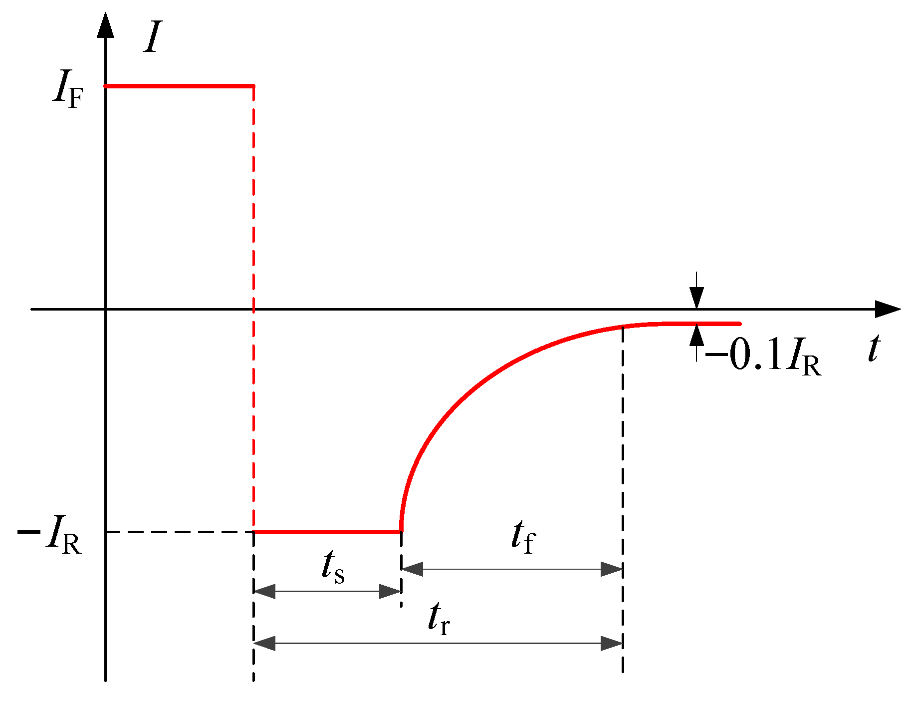
When the voltage at the diode terminal changes from forward to reverse, the current flowing through the diode will be reversed, but it is not immediately reduced to reverse saturation current; on the contrary, it remains basically unchanged for a period of time in the , still in the reverse conduction state and not turned off. For PN junction diodes, the N-region storage hole does not disappear immediately, and the current gradually decreases only through the influence of the decimation of the reverse current and the recombination of the minority carriers (N-region hole).
After the period of , the concentration of holes on the N-zone side of the PN junction is very small, and the storage charge in the N-region is almost completely gone. The gradient of the hole concentration at the boundary gradually decreases, and the reverse current begins to gradually decrease, and then after , the current returns to , and then returns to steady state. The above process is called the diode reverse recovery process, as shown in Figure 1.

Figure 1.
Diode reverse recovery process.
It is generally specified that after the , represents the time it takes when the current drops from to . Among them, is the reverse current flowing through the diode when the applied voltage turns from forward to reverse during the reverse recovery measurement. is called the storage time, called drop time, called reverse recovery time or shutdown time [21].
From Figure 1, we can see that when the working signal of the electronic system changes from forward to reverse, due to this reverse recovery characteristic of the diode, the current flowing through the diode changes from forward to reverse, and the diode reverse current cannot be immediately reduced to zero to reach a complete cutoff state, which will lead to a very large di/dt. According to Maxwell’s equations, this is the cause of the electromagnetic waves. Under the influence of parasitic parameters, these harmonic signals form inrush currents and peak voltages with short pulse periods and high interference intensities, resulting in interference. The diode reverse recovery time can be expressed as:
In the formula, is the minority carrier lifetime.
When the applied voltage to the diode changes, the carrier distribution in the internal barrier region and the two neutral regions changes accordingly, thus creating a capacitive effect, called junction capacitance, which is generally of the order of pF, and decreases with the increase in the applied voltage. The higher the signal frequency, the more significant the junction capacitance effect, so the diode will generate a larger dv/dt for high-frequency signals, and even affect the rising and falling edges of the signal, resulting in conducted interference.
The junction capacitance determines the maximum operating frequency of a diode. When the signal frequency exceeds the maximum operating frequency, the diode will partially or completely lose unidirectional conductivity, resulting in signal distortion and harmonic interference at different frequencies. The diode junction capacitance can be expressed as:
where is the external bias voltage, FC is forward biased barrier capacitance, , , and are the built-in potential, gradient coefficient, and zero-bias barrier capacitance, respectively, and the junction capacitance can be calculated through these three parameters.
Ideally, the functional characteristics of the diode imply unidirectional conduction; that is, the forward low resistance is turned on and the reverse high resistance is turned off. The ideal positive I-V relationship varies exponentially, which can be expressed as:
The previous equation is the famous Schokley equation in semiconductor physics, is the diode applied voltage, is the Boltzmann constant, is the electron charge, is the absolute temperature, at room temperature is the temperature voltage equivalent, and at room temperature , there is .
To consider factors such as the recombination of diode minority carriers in the barrier region, the ideal forward I-V relationship is modified in [22]:
where is the reverse saturation current, is the voltage equivalent of temperature, which is 26 mV at room temperature. N is the emission coefficient that reflects the degree of correction of the actual forward I-V curve close to the ideal curve. The value of N, related to the material of the diode, generally needs to be obtained by measurement.
The ideal reverse I-V characteristic of a diode mainly considers the effect of the diffusion current. In addition, when the applied reverse voltage exceeds a certain value , the current exceeds the reverse breakdown current and rapidly increases exponentially, and the diode undergoes reverse breakdown and loses unidirectional conductivity.
In summary, diodes have dynamic characteristics such as reverse recovery and junction capacitance. At high frequencies, they generate various complex harmonics for the operating signal of the system. These harmonic signals cause conduction interference in the circuit. When the frequency is very high, it passes through the inductor. The coupling of parasitic parameters, such as the capacitance, can even cause radiated interference. At the same time, the nonlinearity of the diode I-V characteristic also affects the signal; therefore, the electromagnetic interference of the diode cannot be ignored.
3. Establishing a Diode EMC Model
3.1. Modeling Process
The diode SPICE model is an EMC model obtained from the perspective of the fundamental equations of semiconductor physics and the approximation of its parameters within a reasonable range. The SPICE model of the diode is mainly composed of two parts: the model equation and the model parameters. The SPICE simulator has established corresponding physical model equations for 16 basic component types and nested them in the software simulation engine. Model parameter files need to be called from the simulation software model library or imported externally, and combined with the simulator for simulation calculations.
The diode EMC model based on “.MODEL” mode mainly includes the 14 model parameters shown in Table 1, of which some model parameters have specific default values or typical values.

Table 1.
The parameters of diode EMC model in “.MODEL” mode.
In general, the 14 model parameters in Table 1 can be divided into three categories: (a) There are static model parameters that reflect the DC characteristics and functional characteristics of the diode: , , , , . Among them, , and characterize the forward bias characteristics of the diodes, and characterize the reverse bias characteristics; (b) The dynamic model parameters that reflect the electromagnetic interference characteristics of diodes are , where , , characterize the relationship between junction capacitance and reverse bias voltage. describes the reverse recovery characteristics, which are affected by the peripheral test circuitry; (c) The model parameters determined by the process or semiconductor material are and the positive partial depletion capacitance correction coefficients that are not affected by other parameters are also attributed to this category, and it is generally believed that according to experience or process materials, they can be directly determined, as known quantities do not need to be optimized.
In the establishment of a comprehensive and accurate diode electromagnetic compatibility model, it is necessary to obtain all the model parameters in Table 1, but usually the diode parameter manual can only provide a part of the parameters; for the model parameters that the parameter manual cannot provide, most of the cases need to obtain the curve of the parameters through testing, and then are further based on the fitting algorithm, the model parameter extraction of the test curve.
The model parameters of the diode junction capacitance characteristics, reverse recovery characteristics and I-V characteristics are derived from the electrical characteristic parameters and curves, which can be obtained by fitting the measured data. An experimental platform is built to test the time-domain waveform of the diode reverse recovery process, so the forward current , the reverse current , reverse recovery time , and then the reverse recovery characteristics can be calculated by Equation (1). In addition, the reverse saturation current temperature index , flicker noise figure , flicker noise index , forbidden bandwidth and forward bias barrier capacitance coefficient are usually classified as model parameters determined by material technology, generally based on semiconductor theory or material technology, which can be directly determined.
After obtaining all the parameters, the diode EMC model can be established according to the SPICE grammar rules. The diode EMC modeling method we propose is shown in Figure 2. The EMC model of the diode obtained by this paper can not only reflect the functional characteristics and electromagnetic interference characteristics of a diode, but also be suitable for computational electromagnetic simulation, which can provide effective technical means and construction ideas for the establishment of various diode EMC models.
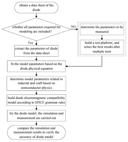
Figure 2.
Flow chart of diode EMC modeling method.
3.2. Nonlinear Fitting Stochastic Optimization Algorithm
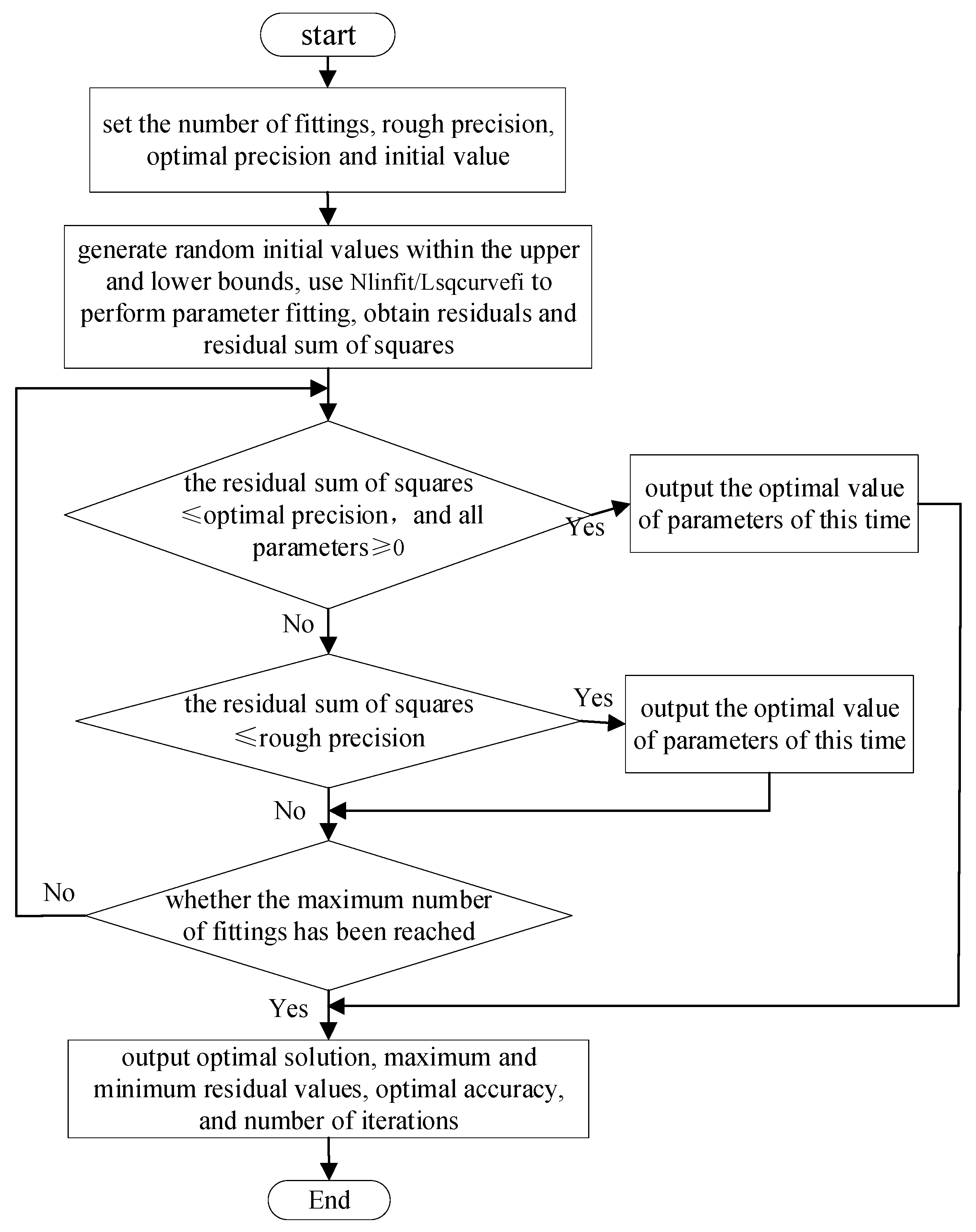
As mentioned above, in general, the diode’s parameter manual does not provide all the parameters needed for modeling, and these missing parameters can only be obtained by the measurement and then by the data fitting method. In this paper, a nonlinear fitting stochastic optimization algorithm is established based on the diode physical characteristic equation, combined with the Nlinfit or Lsqcurvefit function. The algorithm combines Equations (2) and (4) to fit and calculate the model parameters of the I-V characteristics and junction capacitance characteristics and obtain the reverse saturation current , emission coefficient , zero-bias junction capacitance , gradient coefficient and built-in potential . The principle of the optimization algorithm is shown in Figure 3.

Figure 3.
Flow chart of nonlinear fitting stochastic optimization algorithm.
The basic idea of the algorithm is random fitting optimization based on the idea of least squares, so that the fitting objective function (diode physical equation) continues to approach the test data until the residual sum of squares reaches the set accuracy or the number of fittings reaches the loop setting. At the maximum value, the algorithm terminates the calculation and finally obtains the optimal solution of the model parameters. We consider setting the rough residual sum of squares to improve the optimization direction, so that the fitting results gradually approach the target accuracy.
Because the initial value of the model parameters will affect the fitting speed and solution results, it is necessary to provide a reasonable initial value to obtain the optimal solution of the model parameters. The specific initial value solution method used in this study is as follows:
where, , , are the initial value, the upper and lower limits of the limited initial value range, and is a random number in the range of (0, 1) generated by the rand function.
According to the test data, the approximate derivative values of two or three groups of specific points can be obtained approximately, and further combined with the first-order derivatives of Equations (2) and (3) to obtain , , , and , a total of five model parameters, considering the result set as the upper limit of the initial parameter value in the fitting optimization algorithm. In addition, the original default value of the diode SPICE model parameters is selected as the lower limit of the initial value of the fitting algorithm. The influence of the test data on the fitting effect is preliminarily considered, and the reference value of the default value of the diode SPICE model parameters is fully reflected.
3.3. The Measurement of Diode
The electrical performance test of the diode is divided into static electrical parameter test and dynamic electrical parameter test; the static electrical parameter is mainly described by the I-V curve, and the dynamic electrical parameter mainly considers the junction capacitance and reverse recovery characteristics.
The I-V static parameter test system for diodes is shown in Figure 4, which consists of the Agilent 4155B semiconductor parameter analyzer, a semi-automatic probe test bench, and a computer with Agilent EasyExpert software installed. The Agilent 4155B semiconductor analyzer has a current-voltage resolution of 10 fA/μV and a corresponding measurement range of 100 mA/100 V. Agilent EasyExpert test software provides the Agilent 4155B with a full range of diode static parameter testing that controls test instruments and probe stations for fully automated I-V scanning tests in DC or pulse mode. The test layout of the 2CZ106C fast recovery diode is shown in Figure 5.
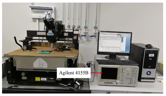
Figure 4.
The I-V static parameter test system for diode.
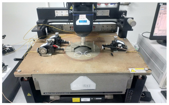
Figure 5.
The I-V static parameter test layout of the 2CZ106C.
2CZ106C is an N-type silicon rectifier diode, and the forward conduction voltage of the silicon diode is about 0.5~0.7 V. Therefore, when testing the forward I-V curve, the set voltage test range is 0~1.5 V, and the current test range is 0~100 mA. In addition, due to the overvoltage protection mechanism of the Agilent EasyExpert test software, the maximum voltage value can be set to −50 V and the maximum measured current value is −10 mA. Therefore, when testing the reverse I-V curve, the reverse test voltage range is −50~0 V, and the test current range is set to −10~0 mA.
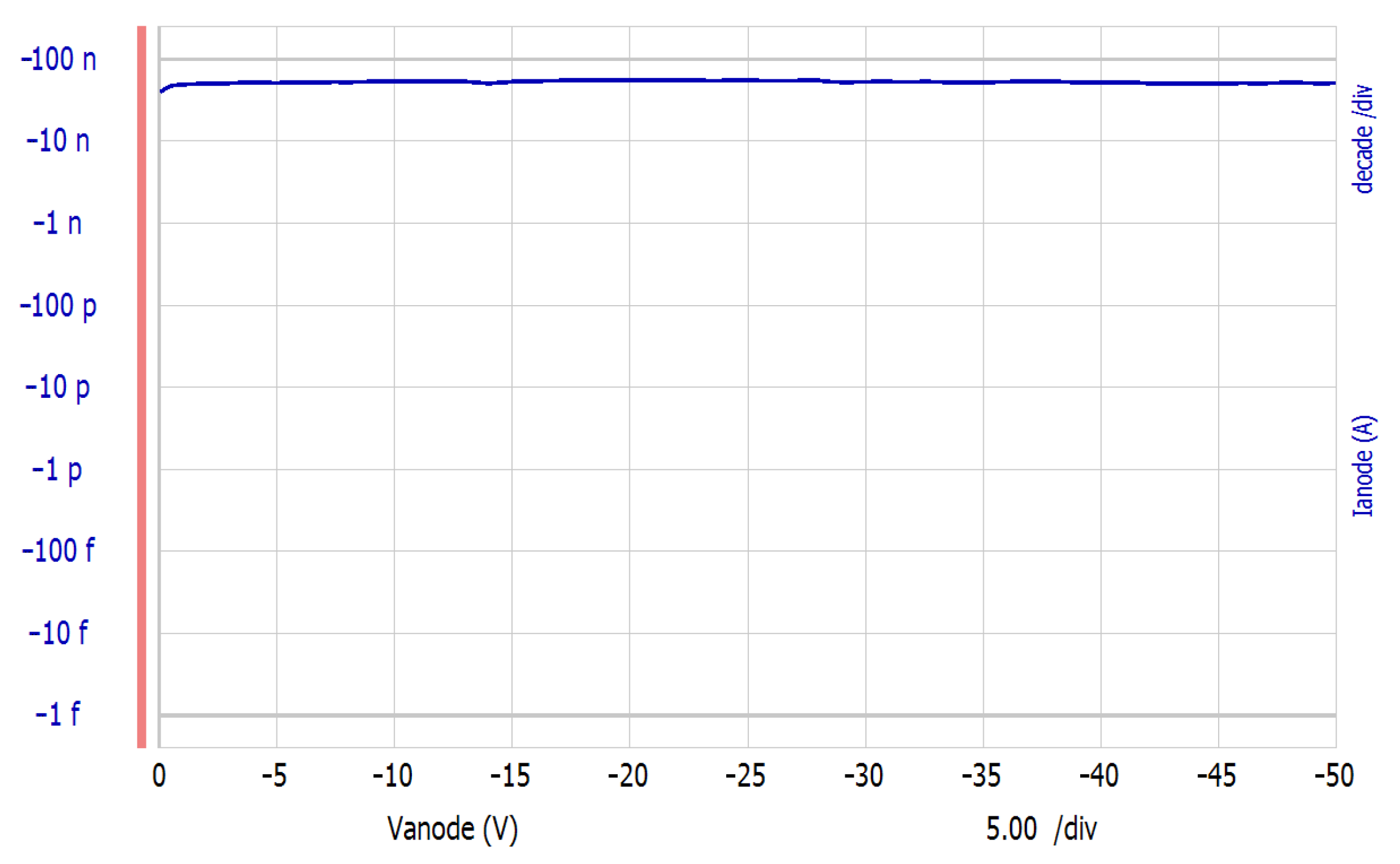
After completing the test system connection, test calibration via Agilent EasyExpert software is also required to eliminate test instrument errors and ensure the accuracy of experimental data. The forward I-V test results are shown in Figure 6, and it can be seen from Figure 6 that at about 1.15 V forward bias, the forward current of the diode 2CZ106C reaches the upper limit current of 100 mA allowed by the instrument, and its opening voltage is about 0.5 V, and the on-voltage is about 0.6~0.7 V. The test results of reverse I-V are shown in Figure 7, where it can be seen that the reverse leakage current of diode 2CZ106C is nA level within the reverse bias voltage of −50 to 0 V (that is, before reverse breakdown).
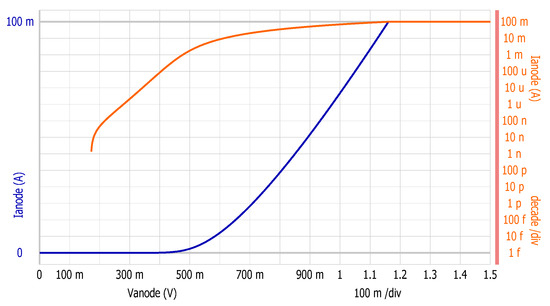
Figure 6.
The forward I-V characteristic curve test results of the 2CZ106C.
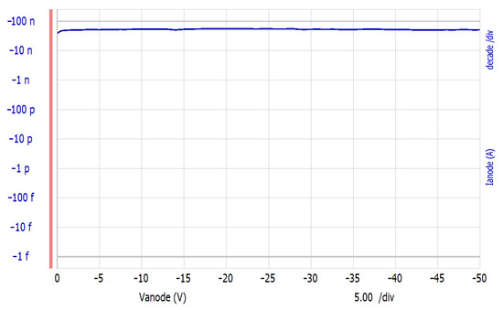
Figure 7.
The reverse I-V characteristic curve test results of the 2CZ106C.
The forward I-V curve of the diode is parameterized by using the Lsqcurvefit nonlinear random optimization algorithm to obtain the optimal solution of the reverse saturation current and emission coefficient, the absolute values of the maximum and minimum residual differences, the sum of squares of the residuals with the best accuracy and the maximum number of iterations as shown in Table 2.
Table 2.
Parameter fitting result of the forward I-V characteristic model of the diode.
For nonlinear random optimization fitting, the difference between the fitted value and the measured value is called the residuals, and the sum of all the residuals squared can be used to measure the goodness of the fit as a whole, and if the value is a very small order of magnitude, close to zero, the fit is good. From the results of Table 2, when the maximum number of cycles = 10000 is reached, the reverse saturation current and the emission coefficient N = 3.087715. The parameter fitting of the Lsqcurvefit nonlinear stochastic optimization algorithm fails to achieve the target optimal residual squared sum and accuracy rsk = 1 × 10⁻¹⁰ originally set by the program, and the actual obtained residual squared sum of squares is 6.302667 × 10⁻⁵. In addition, the absolute value of the maximum current residuals obtained at 0.6585 V of the measured data used is 1.468315 × 10⁻³ A, and the absolute value of the minimum residual current obtained at a voltage of 0.534 V is 2.189795 × 10⁻⁶ A.
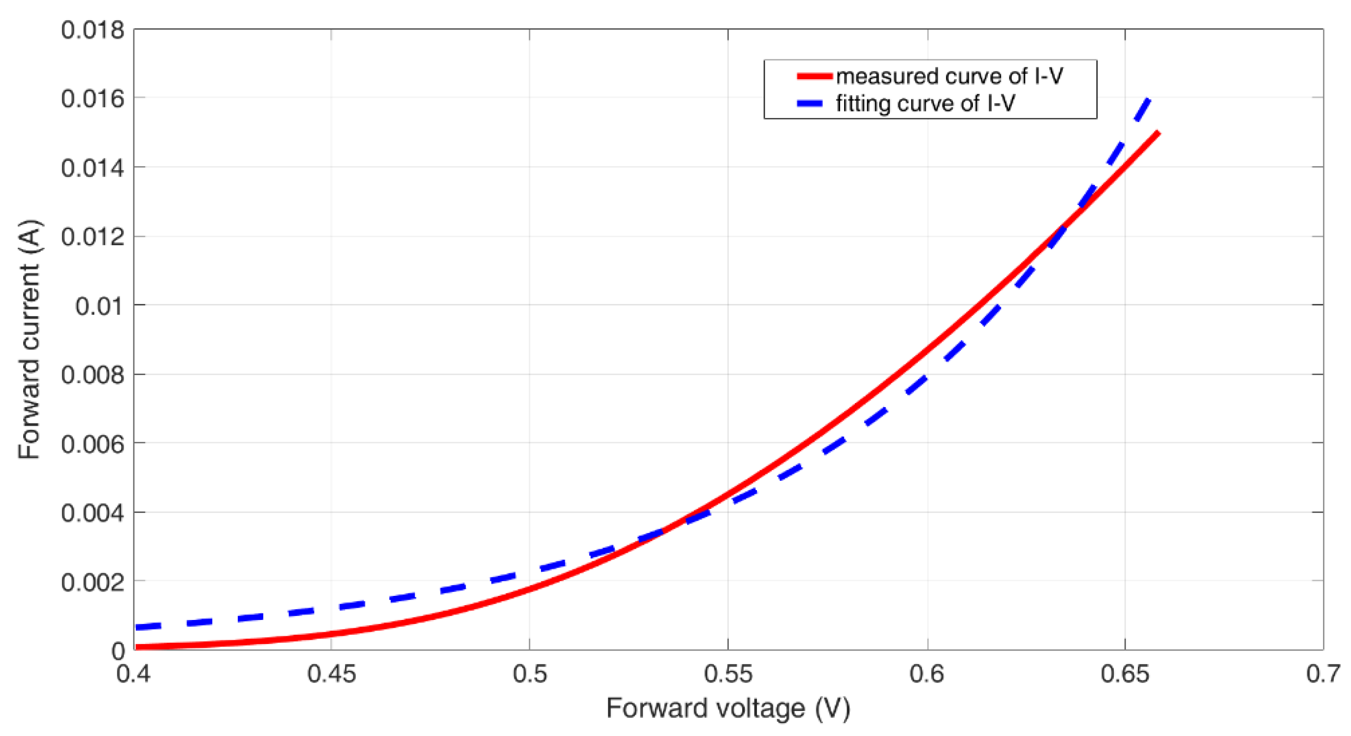
Figure 8 shows the comparison between the fitted curve and the measured curve. It can be seen from Figure 8 that the fitted curve is basically consistent with the measured curve; the two curves are well matched. Therefore, the diode parameters obtained by fitting have high accuracy.

Figure 8.
The comparison between the fitted and measured curve of I-V.
As mentioned earlier, the dynamic parameters of the diode focus on the junction capacitance and reverse recovery time parameters.
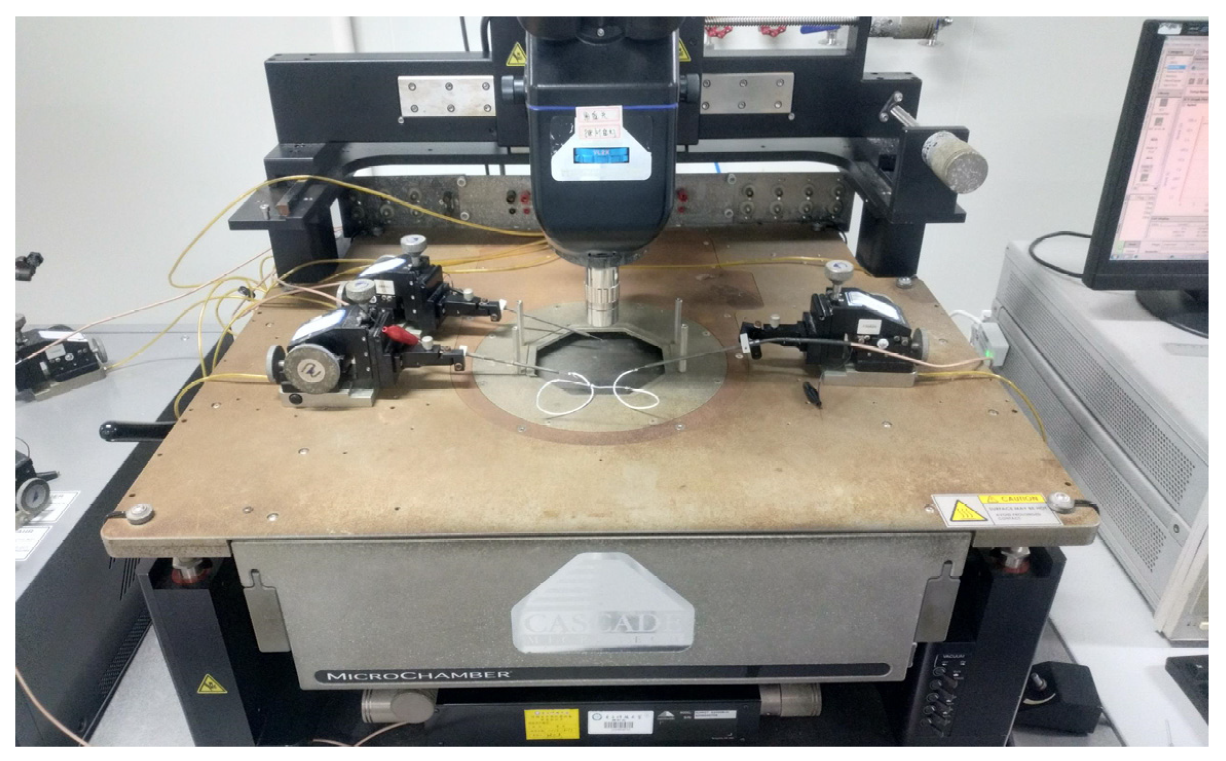
The Agilent 4294A Precision Impedance Analyzer can test components and circuits for electrical characteristics such as impedance curves and junction capacitance curves, and the test accuracy can reach pF level. The Agilent 4294A impedance analyzer is built with the Signaton S-1060 series probe test bench and a computer equipped with the test sharing software QuickTest to form a semiconductor device test system as shown in Figure 9, and the junction capacitance characteristic curve of the diode 2CZ106C is tested experimentally.
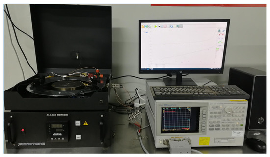
Figure 9.
The junction capacitance parameter test platform for diodes.
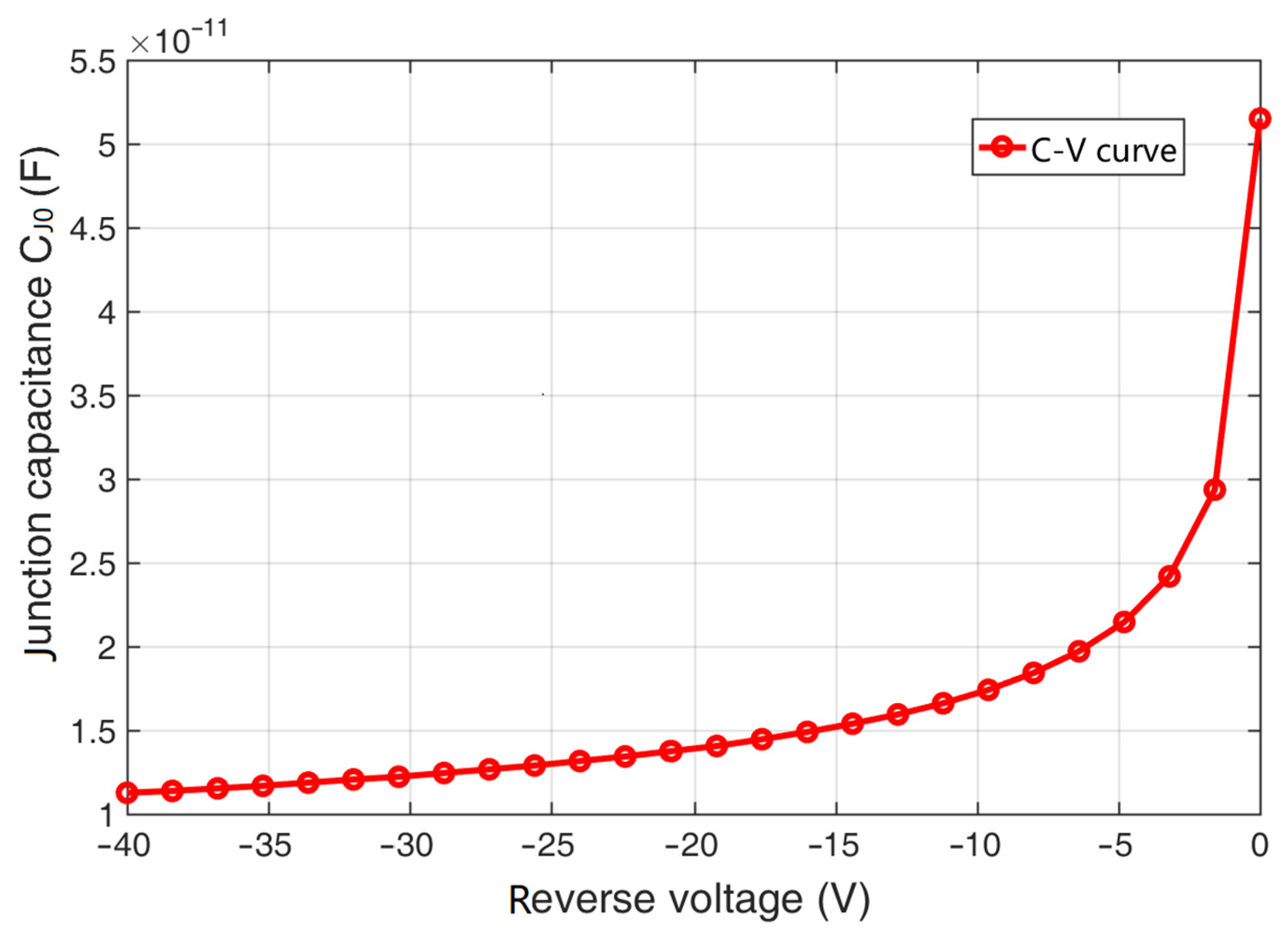
Since the order of magnitude of diode junction capacitors is generally pF level, which is a smaller capacitance, when testing the diode 2CZ106C junction capacitance, we choose a combination of measurement parameters in parallel. The test step is to open the Agilent 4294A impedance analyzer in advance to warm up for at least 20 min, then perform phase compensation, open circuit compensation, short circuit compensation and load compensation, open the test software QuickTest, set the sample information and select the bias parameter for testing. According to the actual environmental conditions, the test temperature is set to 19.6 °C, the sweep bias frequency is 1 MHz, the DC bias range is −40~0 V and the test data point is 26. Only a bias sweep of the diode 2CZ106C junction capacitance curve data can be obtained, so the test parameters are selected and not displayed . The detail of the diode’s junction capacitance parameter test is shown in Figure 10, and the test result is shown in Figure 11.
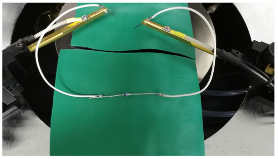
Figure 10.
The detail of the diode’s junction capacitance parameter test.
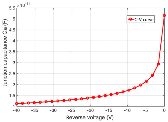
Figure 11.
The junction capacitance test result.
From Figure 11, we find that the diode 2CZ106C junction capacitance decreases with the increase in the applied reverse voltage, and the order of magnitude is generally pF. From this qualitative analysis, the test results basically reflect the characteristics of the diode junction capacitance.
Considering the junction capacitance of the diode in the case of as the objective function, and Nlinfit nonlinear random optimization algorithm is applied to the fitting of diode junction capacitance characteristic model parameters, and the optimal solution of built-in potential , gradient coefficient , zero bias junction capacitance .
First, the derivative values of three groups of specific points are estimated from the experimental data, and then substituted into the first-order derivative expression of the fitting objective function. We observe the values of , and are 1.648 × 10⁻¹¹, 16.545 and 1.636, respectively. The analytical solutions of , and are considered as the upper limit of the initial value in the nonlinear fitting stochastic optimization algorithm, and the typical values are set as the lower limit of the initial value of the fitting.
The absolute value of the maximum and minimum residuals, the sum of the residuals of the optimal accuracy, the maximum number of iterations and other information are shown in Table 3.
Table 3.
Parameter fitting result of the C-V characteristic model of the diode.
As can be seen from Table 3, when the maximum number of cycles t = 10,000 is reached, three model parameters of the diode are obtained: built-in potential = 0.319813, gradient coefficient = 0.315106 and bias junction capacitance = 5.150461 × 10⁻¹¹. The parameter fitting calculation fails to achieve the original target optimal residual squared sum accuracy rsk = 1 × 10⁻³⁰ pF2, and the actual residual squared sum and the optimal accuracy are 2.049740 × 10⁻²⁶ pF2. In addition, the absolute value of the maximum residual value of the capacitor is obtained at a voltage of 1.6 V, Smax = 7.765136 × 10⁻¹⁴ pF, and the minimum residual absolute value Smin = 5.582152 × 10⁻¹⁶ pF is obtained at a voltage of 0.534 V. Both the absolute value of the maximum residuals and the optimal accuracy of the actual residuals are very close to zero, indicating that the curve fitting has a high degree of accuracy.
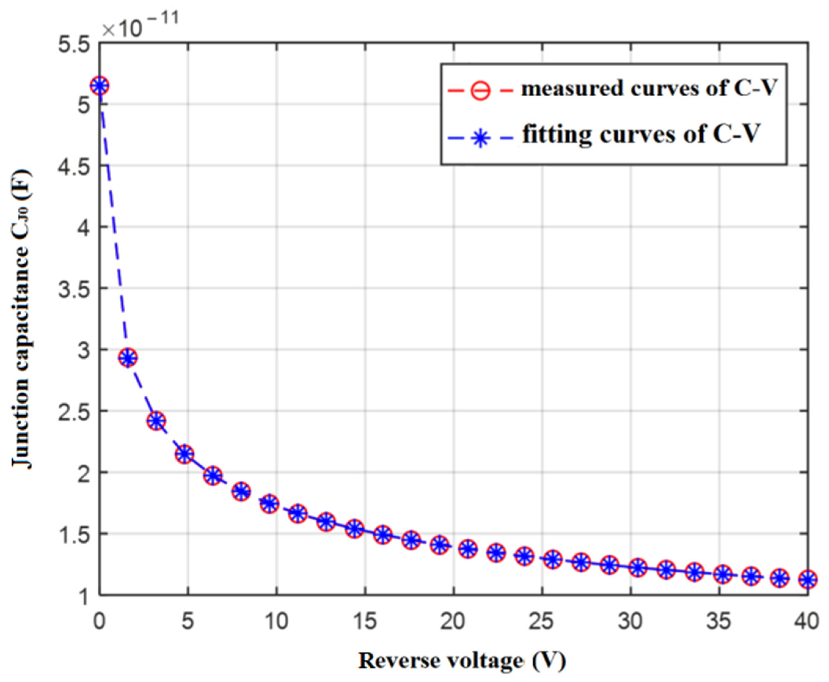
Figure 12 shows the result of comparing the fitted curve of the junction capacitance characteristics with the measured curve. From the figure, it can be seen that the fitted curve is exactly the same as the measured curve.

Figure 12.
Comparison of fitting and measured curves of junction capacitance characteristics.
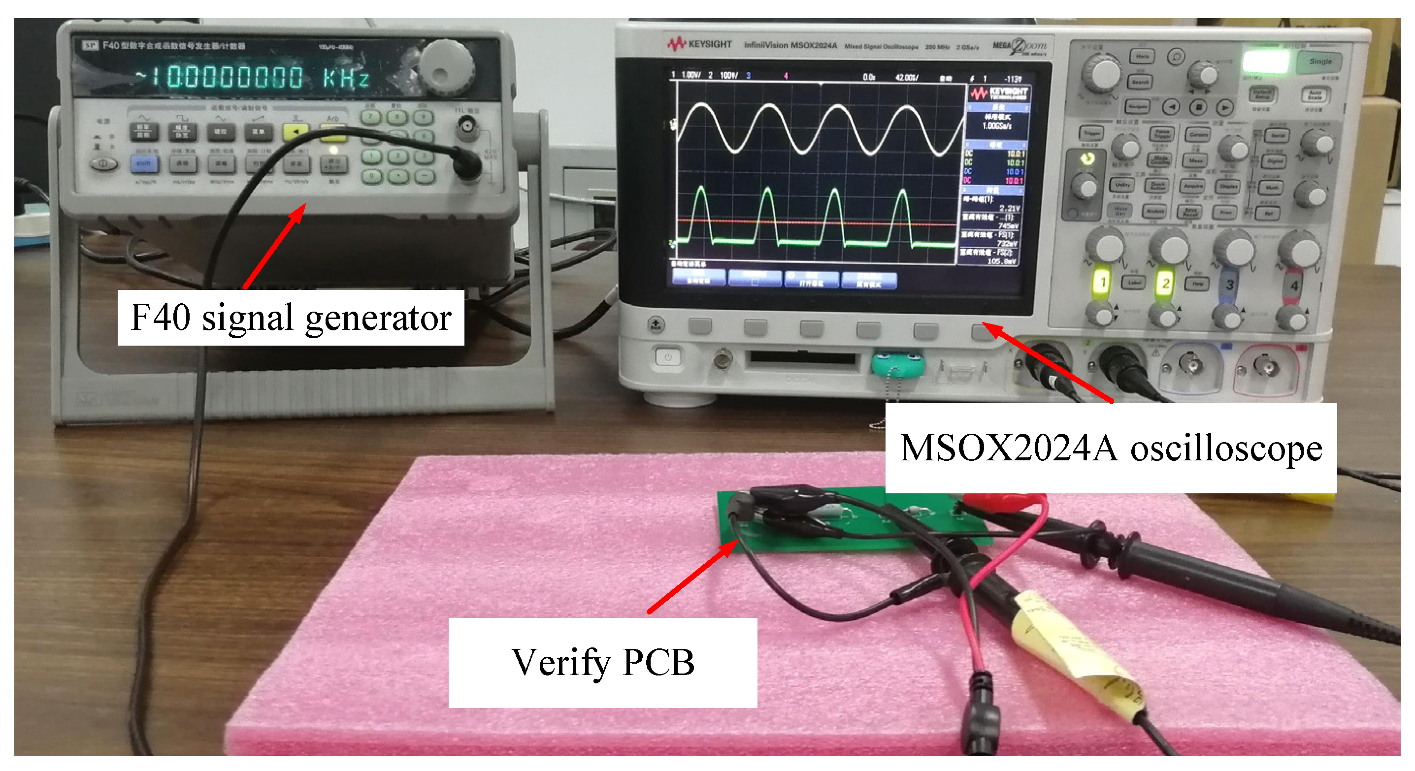
In diode EMC models, reverse recovery characteristics are generally characterized by time-of-flight . The reverse recovery time of diode 2CZ106C can be obtained by building an external circuit test, and the model parameter can be further obtained. For the experimental test of diode reverse recovery time , the square wave with a given duty cycle of 50% can be used as the excitation signal by the F40-type digital synthesis function signal generator. We use the Keysight MSOX2024A mixed-signal oscilloscope to test the time-domain waveform at both ends of the load to obtain the diode reverse recovery process. At the same time, through the two longitudinal wiper of the oscilloscope, the reverse recovery time of the diode is accurately read, and the transition time is solved using the physical formula of the previous section and the test platform is shown in Figure 13.
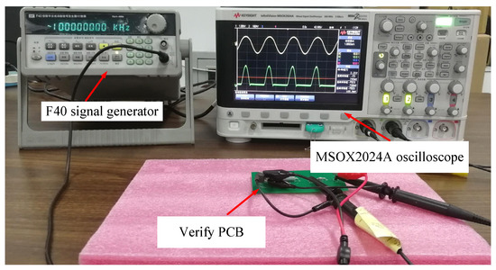
Figure 13.
The reverse recovery characteristics test system for diode.
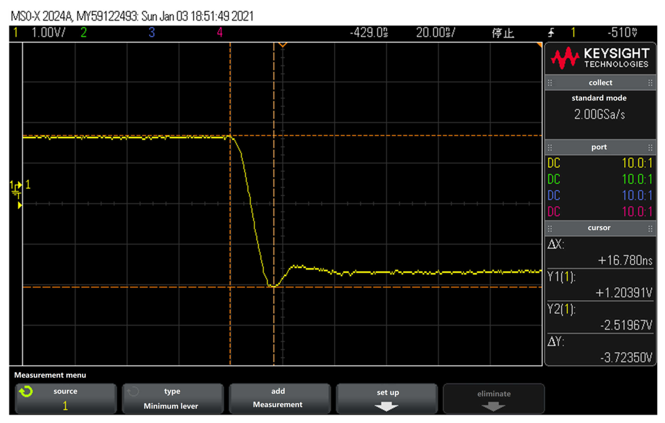
A square wave signal with a frequency of 1 kHz and a peak-to-peak value of 5 V is applied as an excitation; in order to avoid damage to the diode 2CZ106C, the PCB board uses a 100 Ω resistor as the diode series load. The local schematic diagram of the diode 2CZ106C reverse recovery waveform is shown in Figure 14. Among them, the divider of the 100 Ω resistor when the diode is forward bias is 1.20391 V, and the division of the 100 Ω resistor when the diode is reverse biased is −2.51967 V. Combined with the theoretical analysis, it can be calculated that the diode forward current = 0.012 A and the reverse current = 0.0252 A.
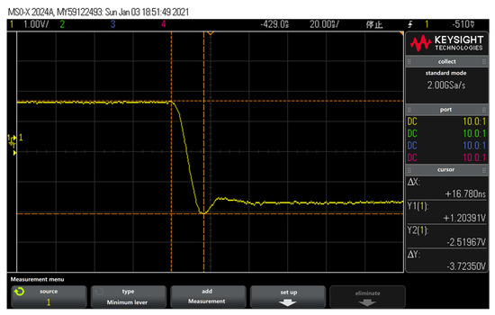
Figure 14.
The reverse recovery waveform of 2CZ109C diode.
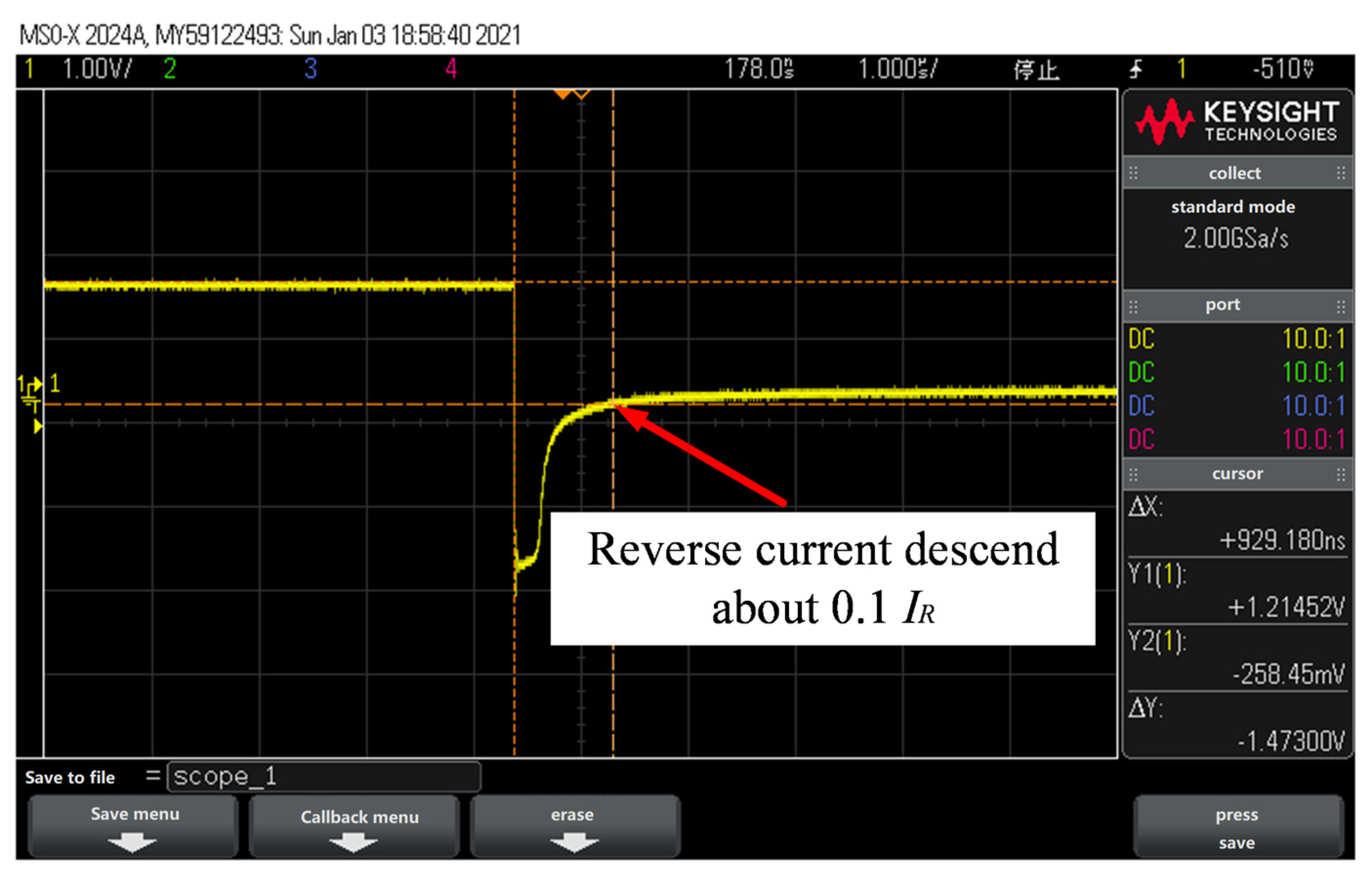
When the applied bias voltage is suddenly reversed, the diode current is also suddenly reversed, and the reverse current of is constant over time, then the current slowly becomes smaller, and then over time, the reverse current drops to . It is shown that when the reverse division of a 100 Ω resistor is about −0.251967 V, the diode is turned off in reverse. The diode 2CZ106C reverse recovery time can be read by the oscilloscope travel standard, as shown in Figure 15, and the diode 2CZ106C reverse recovery time is 9.2918 × 10⁻⁷ s.

Figure 15.
Test results of reverse recovery time .
Therefore, the transit time characterizing the reverse recovery characteristic can be calculated by Equation (6).
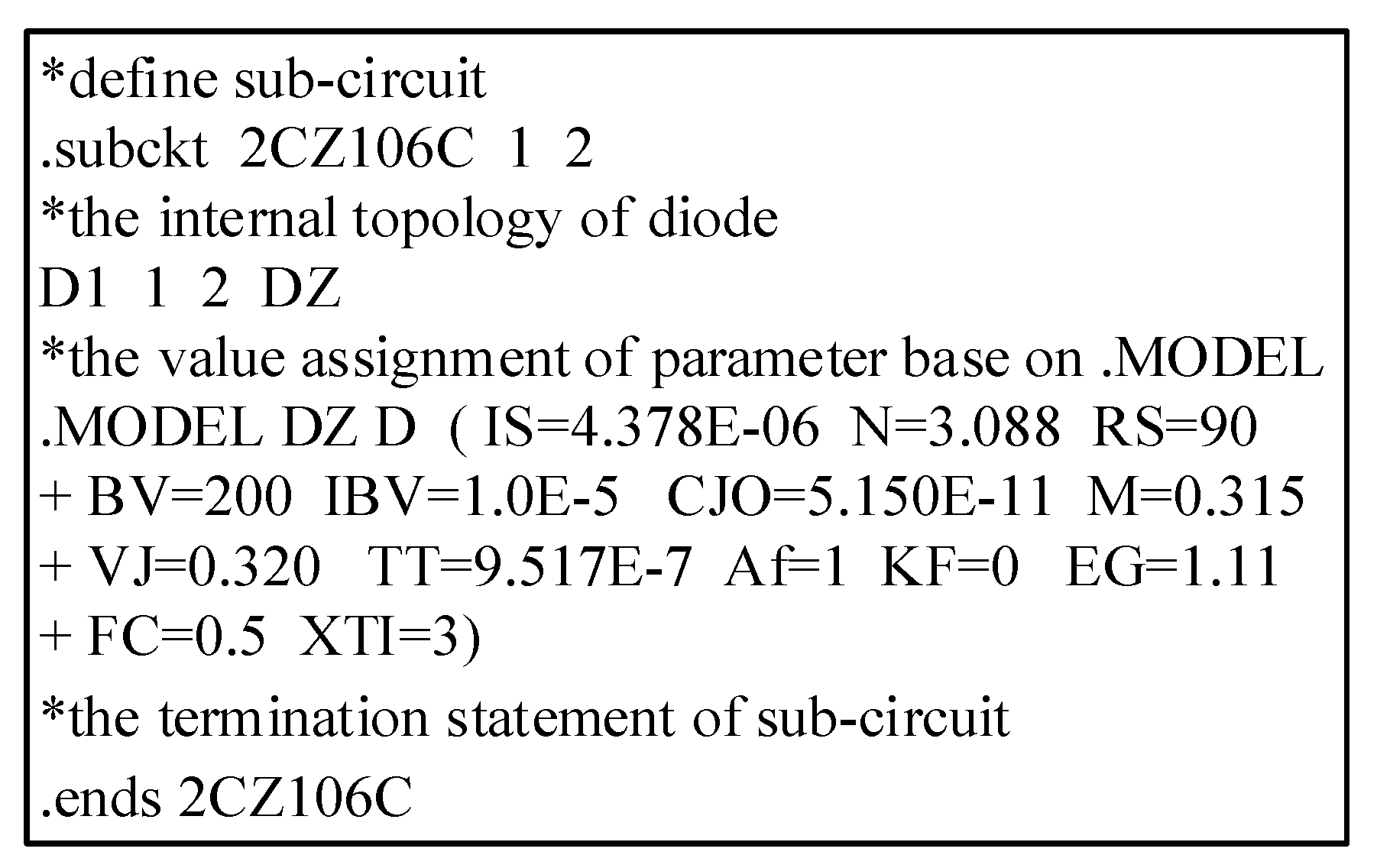
3.4. Establishment of Diode Electromagnetic Compatibility SPICE Model
Through the test and data fitting method mentioned above, we obtain 6 of the 14 parameters necessary for diode modeling, and the other parameters can be obtained through the data sheet.
According to the electrical characteristics provided by the data sheet, the reverse breakdown voltage and reverse breakdown current of the diode 2CZ106C are determined to be 200 V and 10 , respectively.
The series resistance of the diode at high frequency is and not pure resistance. To consider parasitic inductance and capacitance, the impedance frequency curve of the diode is tested using an impedance analyzer. The results show that the constant impedance of the diode in the frequency band below 10 MHz is about 90 Ω. To consider the influence of the parasitic parameters of the diode on the high-frequency operating signal, the series resistance is set to 90 Ω.
According to the semiconductor theory, the model parameters determined by the material process can be directly determined without optimization. Therefore, the reverse saturation current temperature index , forbidden band width , flicker noise figure , flicker noise figure and forward biased barrier capacitance coefficient are all default values. In summary, the parameter values of the diode 2CZ106C model obtained through fitting calculation and analysis are shown in Table 4.
Table 4.
Model parameters of diode 2CZ106C.
After obtaining the parameters necessary for diode modeling above, we can establish the electromagnetic compatibility model of the diode 2CZ106C according to SPICE grammar rules, as shown in the Figure 16.

Figure 16.
The EMC model of the diode 2CZ106C.
4. Model Simulation and Verification
4.1. Design of Model Verification Platform
The PCB board, shown in Figure 17, is designed and fabricated. To avoid introducing errors caused by too many other components, only 100 Ω resistors are used as loads to protect the diodes, which are shown in Figure 13; the model verification platform uses a signal generator to provide different frequency excitation signals and an oscilloscope to test the time-domain waveforms.
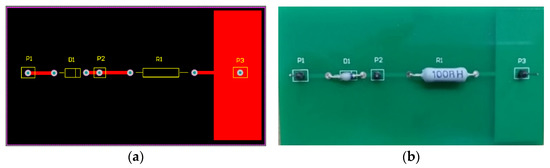
Figure 17.
PCB board for model verification (a) design drawing; (b) Processed circuit board.
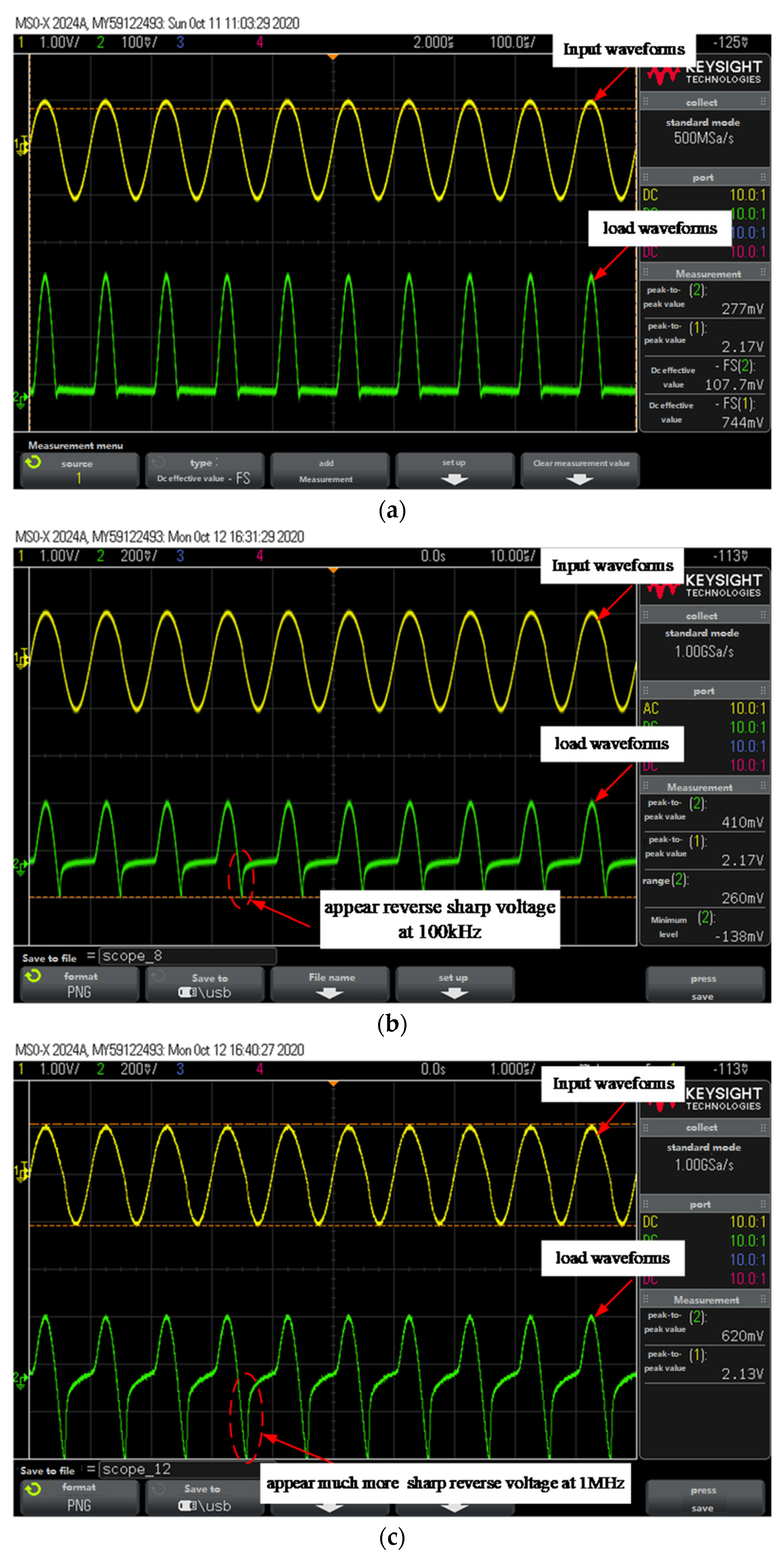
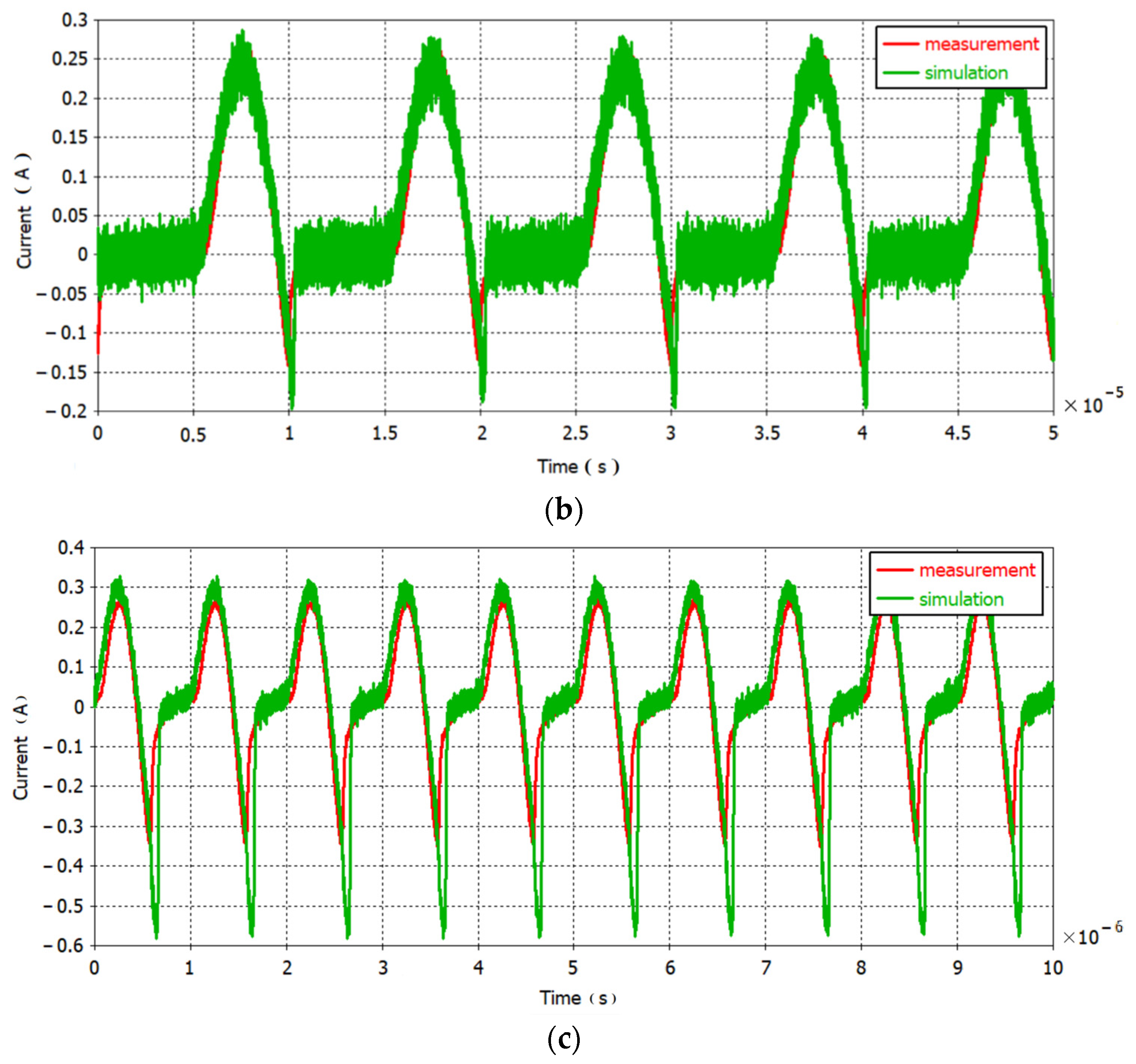
To ensure that the input signals of the simulation and test are consistent, two channels are used to test and save the signals at the input end and load end of the PCB board, respectively, as the excitation signal for the subsequent simulation. Figure 18a–c shows the time-domain waveforms of the input end (one channel) and load end (two channels) of the PCB board when the signal frequencies are 10 kHz, 100 kHz and 1 MHz, respectively.
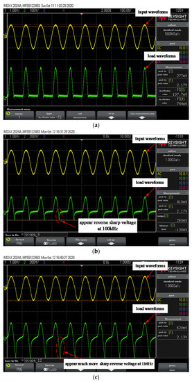
Figure 18.
Experimental test results: (a) Input and load waveforms of 10 kHz excitation; (b) Input and load waveforms of 100 kHz excitation; (c) Input and load shape of 1 MHz excitation.
It can be seen that when the frequency of the excitation signal increases, the waveform of the load terminal is gradually distorted. The higher the frequency, the more irregular the waveform, which is caused by diode junction capacitance and reverse recovery characteristics.
From Figure 18, we can also see that when the excitation signal frequency is 10 kHz, the load resistor can achieve a half-wave output, indicating that the diode 2CZ106 can achieve good single guide passivity. When the excitation signal frequency is 100 kHz, the diode 2CZ106 does not fully achieve single passivity, although the shutdown time is short, but there is a large reverse voltage at the load resistor, with a peak value of about 0.15 V. When the excitation signal frequency reaches 1 MHz, the diode 2CZ106 loses almost single conductivity and there is a larger reverse voltage at the load resistor, with a peak of about 0.3 V.
4.2. Comparison with Simulation
The following is a comparison of simulation and test results. First, the diode verification PCB design file shown in Figure 17a is imported from the Altium Designer software into the CST PCB studio. In the import settings of CST, some unimportant components can be removed, thereby simplifying model complexity and improving simulation speed. After importing the PCB design file, we use the 2D TL Modeling function in CST PCB studio to generate the equivalent circuit model corresponding to the PCB board, as shown in Figure 19.
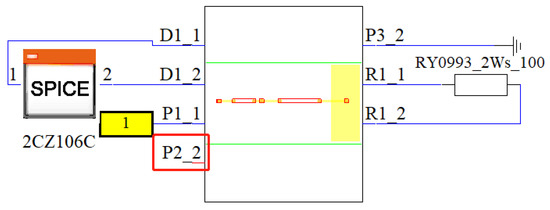
Figure 19.
The complete simulation circuit established in CST.
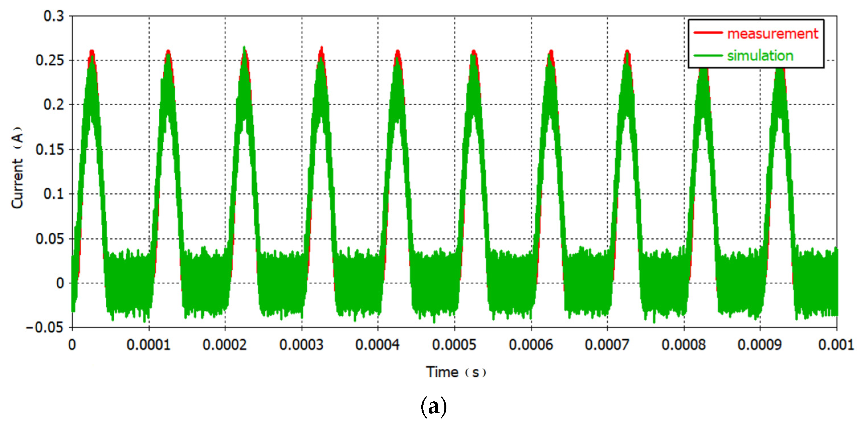
The time domain signal at the input terminal of the PCB board shown in Figure 17 is used as the excitation source of the simulation model, and the time-domain waveform results of the simulation and measurement results are shown in Figure 20.
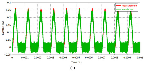
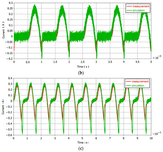
Figure 20.
Comparison of measured and simulated in time-domain: (a) 10 kHz; (b) 100 kHz; (c) 1 MHz.
From the comparison of the above time-domain results, when the sinusoidal signal with a given frequency of 10 kHz is used as an excitation, the time-domain waveform results calculated by experimental testing and simulation are well matched. When the excitation signal frequency is 100 kHz and 1 MHz, there is a reverse voltage in the time-domain waveform of the measurement and simulation, and there is a slight error in their coincidence but the trend is basically the same.
This slight error may be due to the following reasons: First, the model parameter that reflects the reverse recovery characteristics of the diode is the transition time . From Equation (1), only a few parameters are considered to calculate the reverse recovery characteristics and these cannot fully reflect the reverse recovery process at high signal frequencies; Secondly, the data of the reverse recovery characteristics are mainly derived from measurements, and then the transition time TT is calculated by theoretical formulas. This process may introduce certain experimental errors, and the assumptions made in the derivation of theoretical formulas ignore the influence of some practical factors; Finally, the transition time TT has been modified during modeling, due to the irregularity of the internal carrier motion of the diode and the complexity of the internal electric field distribution, and there may still be some modeling errors after the approximate correction.
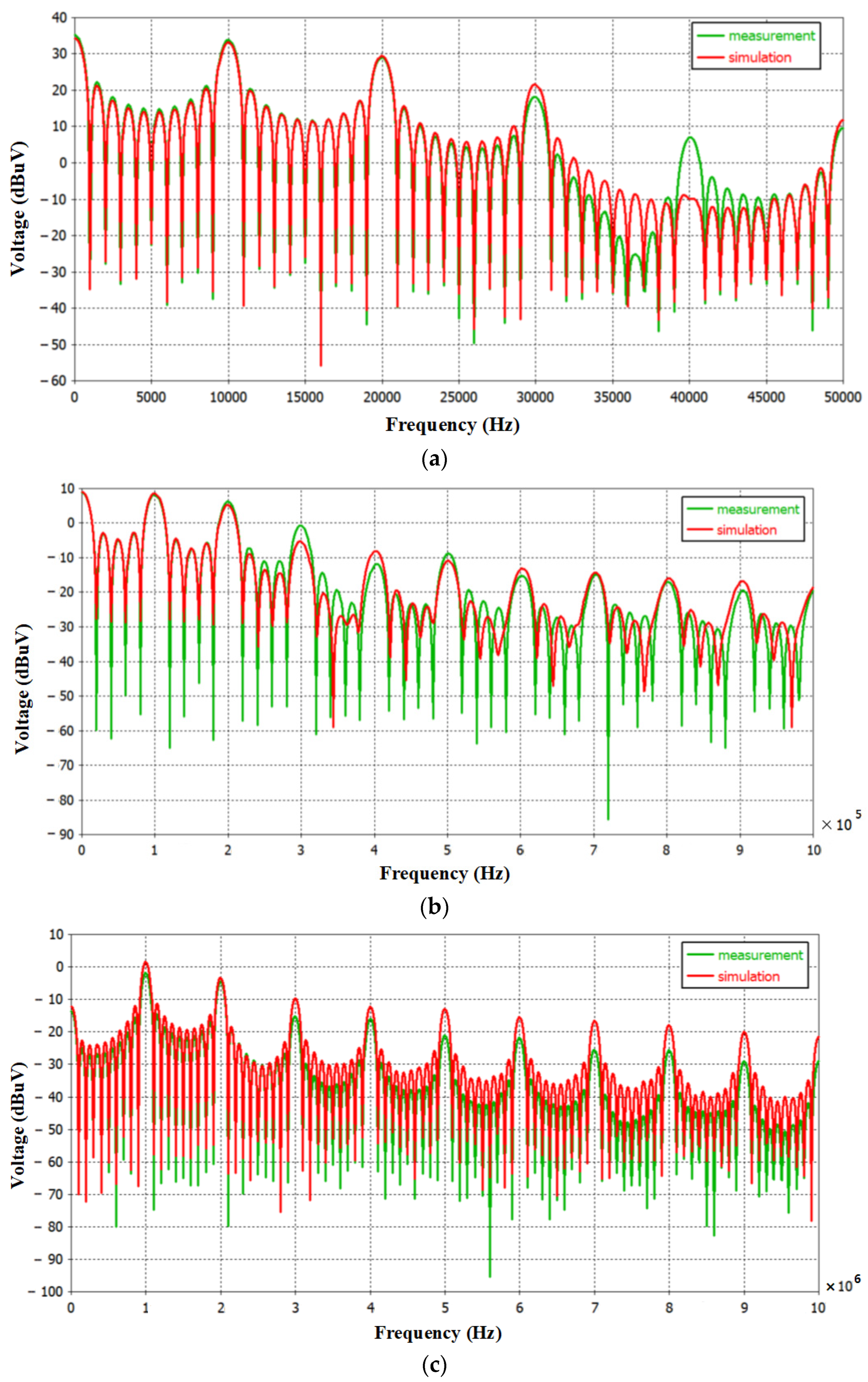
Considering that the measured time-domain waveform is not a standard sine wave, there are harmonic components in different frequency bands. By comparing the measured and simulated frequency components and the amplitude components of each frequency component, it can be verified whether the diode EMC model accurately reflects its related characteristics in the frequency domain. Therefore, the simulated and measured time-domain waveforms are converted into spectrum results by the fast Fourier transform function of CST, as shown in Figure 21.
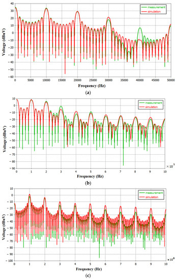
Figure 21.
Frequency domain comparison of measured and simulated results: (a) 10 kHz; (b) 100 kHz; (c) 1 MHz.
As can be seen from Figure 21, the spectral results of the experiment and simulation are generally in good agreement, and the effective frequency band near the fundamental frequency of 10 kHz, 100 kHz and 1 MHz is almost identical. Some valuable conclusions are: (1) Comparing the 10 kHz spectrum results, the frequency domain results of experiments and simulation are completely consistent in the frequency band below 2 times the fundamental frequency (20 kHz), and there is a certain error in the noise harmonic higher than the 2 times fundamental frequency, but the overall difference is not large; (2) Compared with the 100 kHz spectrum results, it is known that the frequency domain results of experimental testing and simulation are completely consistent in the frequency band below 2 times the fundamental frequency (200 kHz), and the noise harmonic higher than the 2 × fundamental frequency has a small error; (3) Compared with the 1 MHz spectrum results, it is known that the frequency domain results of experimental testing and simulation calculation are completely consistent in the frequency band below 3 times the fundamental frequency (3 MHz), and there is a certain error in the noise harmonics above 3 times the fundamental frequency, but the overall difference is not much.
In order to quantitatively analyze the difference between simulation results and test results, the Feature Selective Validation (FSV) method is applied [23,24]. The FSV technology is an IEEE standard that shows the correlation between two sets of data according to a specific standard, which is widely used in the field of electromagnetic simulation [25,26]. The FSV technical evaluation index mainly includes: total amplitude difference measure (ADM), total characteristic difference measure (FDM) and total global difference measure (GDM). According to the ADM, FDM and GDM sizes, the degree of conformity between the data is described as excellent (0–0.1), very good (0.1–0.2), good (0.2–0.4), fair (0.4–0.8), poor (0.8–1.6) and very poor (>1.6). The simulation and measurement results in time-domain are analyzed based on FSV method, as shown in Table 5.
Table 5.
The FSV evaluation results of the proposed method.
From Figure 20 and Figure 21 and Table 5, we can comprehensively see that the improvement of the SPICE model of the diode can reflect its actual work, and can ensure that the test and simulation calculation results are completely consistent in a certain frequency band, although there are some errors in the higher harmonics, but the overall difference is not large; it can be concluded that this method has high accuracy.
5. Conclusions
In this study, a method for establishing an electromagnetic compatibility model of diodes based on physical equations is proposed. Compared with the CST software library model, the model in this study can truly reflect the gradual process of diode reverse cut-off and the peak voltage generated by dynamic characteristics. A comparison of the measured and simulated results from the time and frequency domains shows that the model in this study not only truly reflects the peak voltage generated by the electromagnetic interference characteristics of the diode, but also ensures that the measured and simulated components match within three times the fundamental frequency on the basis of accurately simulating the actual working conditions. The internal harmonic components and amplitudes of each component are completely consistent, and the model has a high electromagnetic compatibility simulation accuracy.
Future work could be carried out on the following aspects:
- (1)
- This paper only considers the temperature effect of reverse current and reverse breakdown voltage; in fact, the diode is thermally sensitive as a semiconductor device, and its forward current and forward conduction voltage will also be affected by temperature. Therefore, to more accurately consider the temperature characteristics of the diode, it is necessary to consider that the analog forward characteristics are affected by temperature.
- (2)
- The influence of reverse recovery time is considered in the modeling of this paper, but with the advent of the 5G era, positive guidance may also interfere with high-frequency signals, which is worth studying in the electromagnetic simulation calculation of high-speed electronic systems.
Author Contributions
Conceptualization, methodology, validation, writing—original draft preparation, D.R. and G.X.; investigation, J.-Q.L.; data curation, Z.-Y.P. and X.Z.; writing—review and editing, D.R. and G.X.; supervision, P.-A.D.; funding acquisition, D.R. All authors have read and agreed to the published version of the manuscript.
Funding
This work was supported by the Major National Science and Technology Fund of China under Grant No. J2019-V-0012-0107, the Innovation and Development Fund of China Academy of Engineering Physics under Grant No. CX20210032, the Institute of Electronic Engineering Project Grant No. J21H-TS 02.
Data Availability Statement
Not applicable.
Conflicts of Interest
The authors declare no conflict of interest.
References
- Ramdani, M.; Sicard, E.; Boyer, A.; Dhia, S.B.; Whalen, J.J.; Hubing, T.H.; Wada, O.; Coenen, M. The Electromagnetic compatibility of Integrated Circuits-Past, Present, and Future. IEEE Trans. Electromagn. Compat. 2009, 51, 78–100. [Google Scholar] [CrossRef]
- Chew, W.C. Marriage of Computational Electromagnetics and Electromagnetic Compatibility. In Proceedings of the 2018 Joint IEEE EMC and APEMC symposium, Singapore, 14–17 May 2018. [Google Scholar]
- Chew, W.C. Maxwell’s Equations and Modern Electromagnetics after 150 Years and Role of Electromagnetics in EMC. In Proceedings of the IEEE APEMC Conference, Shenzhen, China, 18–21 May 2016. [Google Scholar]
- Leila, F.; Anis, A. New simplified model for predicting conducted EMI in DC/DC converters. Electr. Eng. 2017, 99, 1087–1097. [Google Scholar]
- Kurt, M.C.; Arnold, J.R.; Pieter, G.W. The Measurement and SPICE Modelling of Schottky Barrier Diodes Appropriate for Use as Bypass Diodes within Photovoltaic Modules. Energies 2022, 15, 4783. [Google Scholar] [CrossRef]
- Ge, K.; Liping, J. Analog and Digital Circuits, 3rd ed.; Publishing House of Electronics Industry: Beijing, China, 2015; pp. 8–20. [Google Scholar]
- Antognetti, P.; Giuseppe, M. Semiconductor Device Modeling with SPICE; McGraw Hill: New York, NY, USA, 1988; pp. 11–40. [Google Scholar]
- Deveney, M. A temperature dependent SPICE macro-model for Zener and avalanche diodes. In Proceedings of the 34th Midwest Symposium on Circuits and Systems, Monterey, CA, USA, 14–17 May 1991; pp. 15–26. [Google Scholar]
- Bley, M.; Filho, M.; Raizer, A. Modeling transient discharge suppressors. IEEE Potentials 2004, 23, 43–45. [Google Scholar]
- Lepkowski, J.; Lepkowski, W. Evaluating TVS Protection Circuits with SPICE. Power Electron. Technol. 2006, 32, 44–49. [Google Scholar]
- Piotrowski, R. An improved Spice2 Zener diode model for soft-region simulation capability. IEEE Trans. Comput.-Aided Des. Integr. Circuits Syst. 1988, 7, 1301–1303. [Google Scholar] [CrossRef]
- Zhang, D.; Brown, R.; Growden, A.; Berger, P.R.; Droopad, R. A Nonlinear Circuit Simulation of Switching Process in Resonant-Tunneling Diodes. IEEE Trans. Electron Devices 2016, 63, 4993–4997. [Google Scholar] [CrossRef]
- Tohlu, M.; Aoki, M.; Takashi, H.; Wada, O. Equivalent circuit model with nonlinear characteristics of Zener diode extracted from SPICE model for ESD simulation. In Proceedings of the International Workshop on the Electromagnetic Compatibility of Integrated Circuits, St. Petersburg, Russia, 4–8 July 2017; pp. 61–65. [Google Scholar]
- Gan, Z. Simplified Zener Diode DC Spice Model. U.S. Patent 20160203250 A1, 14 July 2016. [Google Scholar]
- Hitchcock, C.W.; Zhou, X.; Pande, G.; Ghandi, R.; Bolotnikov, A.; Chow, T.P. A Subcircuit SPICE Model for SiC Charge-Balance Schottky Diodes. Mater. Sci. Forum 2020, 1004, 945–952. [Google Scholar]
- Yunyeong, C.; Miryeon, K.; Jisun, P.; Shin, H. Analysis of Organic Light-Emitting Diode SPICE Models with Constant or Voltage-Dependent Components. J. Nanosci. Nanotechnol. 2020, 20, 4773–4777. [Google Scholar]
- Tao, L.; Le, X.; Yao, H.; Wu, H.; Yang, Y.; Wu, N.; Wei, F.; Shi, X.; Yang, X. A Novel Simulation Method for Analyzing Diode Electrical Characteristics Based on Neural Networks. Electronics 2021, 10, 2337. [Google Scholar] [CrossRef]
- Yingjie, J.; Fei, X.; Yaoqing, D.; Yifei, L. Field-circuit Coupling Modeling and Multi-rate Electro-thermal co-simulation Analysis of Merged PiN Schottky SiC Diode. Proc. CSEE 2019, 39, 5585–5594. [Google Scholar]
- Qiang, L.; Haijing, Z.; Fukai, X.; Zhenguo, Z. Research on Electromagnetic Interference of Switch Power Supply Based on PIN Diode Model. J. Microw. 2014, S2, 29–32. [Google Scholar]
- Chengkai, W. Research on Terahertz Frequency-Multiplied Technology Based on Schottky Diodes. Master’s Thesis, University of Electronic Science and Technology of China, Chengdu, China, 2018; pp. 14–24. [Google Scholar]
- Xingbi, C.; Yong, C. Microelectronic Devices, 3rd ed.; Publishing House of Electronics Industry: Beijing, China, 2018; pp. 70–74. [Google Scholar]
- Enke, L.; Binsheng, Z.; Jinsheng, L. Semiconductor Physics, 7th ed.; Publishing House of Electronics Industry: Xi’an, China, 2008; pp. 181–185. [Google Scholar]
- IEEE Std. 1597.1-2008; IEEE Standard for Validation of Computational Electromagnetics Computer Modeling and Simulations. IEEE: New York, NY, USA, 2008; pp. 1–41.
- IEEE Std. 1597.2-2010; IEEE Recommended Practice for Validation of Computational Electromagnetics Computer Modeling and Simulations. IEEE: New York, NY, USA, 2011; pp. 1–124.
- Alistair, D.; Gang, Z.; Slawomir, K.; Wang, L. Objective Selection of Minimum Acceptable Mesh Refinement for EMC Simulations. IEEE Trans. Electromagn. Compat. 2015, 57, 1266–1269. [Google Scholar]
- Alistair, D.; Gang, Z.; Slawomir, K.; Orlandi, A.; Di Febo, D.; Wang, L.; Sasse, H. Comparison of Data with Multiple Degrees of Freedom Utilizing the Feature Selective Validation Method. IEEE Trans. Electromagn. Compat. 2016, 58, 784–791. [Google Scholar]


Publisher’s Note: MDPI stays neutral with regard to jurisdictional claims in published maps and institutional affiliations. |
© 2022 by the authors. Licensee MDPI, Basel, Switzerland. This article is an open access article distributed under the terms and conditions of the Creative Commons Attribution (CC BY) license (https://creativecommons.org/licenses/by/4.0/).