1. Introduction
Switched-mode power supplies SMPS cause electrical noise due to their fast
and
. Depending on the power requirement and voltage conversion, a variety of SMPS concepts exist. Boost, buck, and flyback converters are widely used. The inverting buck/boost topology is often used in display drivers for AMOLED displays. AMOLED displays need two positive and one negative supply lines. The positive supply lines are often controlled by buck converters, while the negative is controlled by an inverting buck/boost converter [
1].
The different topologies are shown in
Figure 1. Each topology had its own electromagnetic compatibility EMC properties. For example, the electromagnetic interference EMI performance of isolated flyback converters is often dominated by the interwinding capacitance [
2,
3,
4,
5]. For boost and buck converters, the inductor isolates either the input or the output side from switching noise. In a buck converter, most switching noise is visible at the input [
6], while for a boost converter, the position of the inductor causes most switching noise to appear at the output [
7]. An inverting buck/boost converter uses an inductor connected to the ground. Thus, the switching noise appears at both the input and the output of the circuit.
The authors of [
8] focused on the modeling of and reduction in radiated emissions using a cross-capacitor and an improved printed circuit board PCB layout.
This paper presents the analysis of the conducted EMI for a converter of this kind. The analysis is based on the simulation and measurements of a converter produced with discrete components and of integrated commercial converters. The measurements and simulations show two distinct resonances, and identify the components and associated parasitics that determine the ringing frequencies during turn-on and turn-off.
2. Brief Description of the Inverting Buck/Boost Topology
The inverting buck/boost converter creates a negative output voltage from a positive input. Its magnitude can be either higher or lower than the magnitude of the input voltage.
The basic elements of the simple inverting buck/boost topology in
Figure 1d are a transistor operated as a switch, a diode, an inductor, an output capacitor, and a controller integrated circuit IC that generates the pulse width modulation PWM signal and controls the gate of the MOSFET. Other more complex topologies can be found in the literature. For higher power, synchronous buck/boost converters are used. Here, the diodes were substituted with a second transistor. Therefore, diode losses were reduced. There also exist advanced concepts to increase the voltage range of the converter [
9] or lower the input current ripple [
10]. However, in this article, we discuss the basic topology in order to understand the fundamental generation of resonances within the circuit.
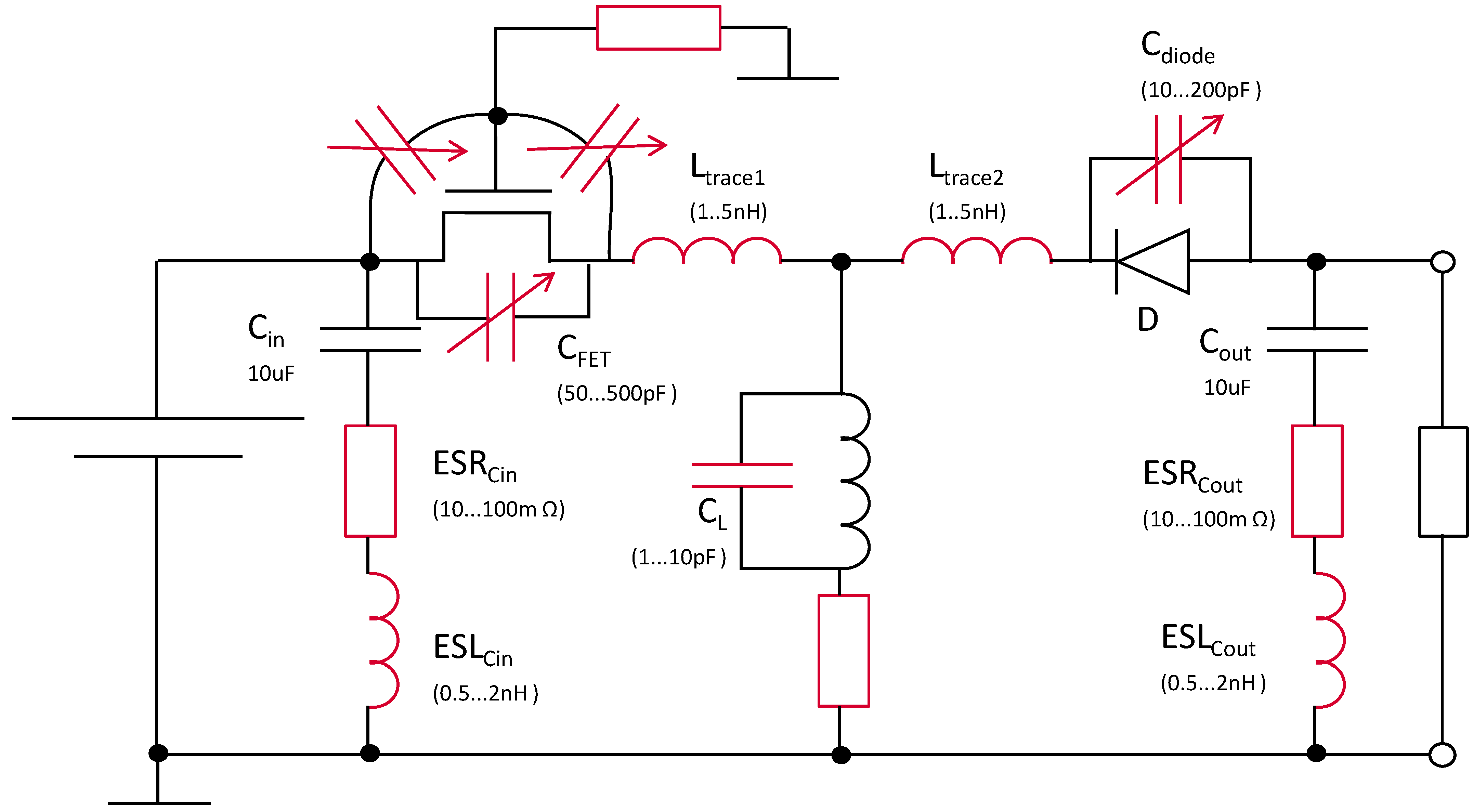
3. EMI Path of the Inverting Buck/Boost Converter
By extending the circuit of the inverting buck/boost converter with a set of parasitic components (
Figure 2) of the different devices and the circuit board, the EMI paths to input and output can be analyzed. The parallel capacitance of the inductor is usually less than 10
and often only a few
. It does not shunt a significant current to ground. Its value is less than the capacitance of the diode. This allows for EMI noise to be visible at both the input and the output.
The following parasitics were added to the circuit:
MOSFET capacitance in its open stage (50 to 500 ).
Diode capacitance in its open stage (10 to 200 ).
The inductance of the loop, which is formed by the input capacitor, the path through the transistor to the diode, and via the diode, and the output capacitor back to the ground plane were broken down into , , , .
The Equivalent Series Inductance ESL and Equivalent Series Resistance ESR of the output and the input capacitors allow for a voltage drop along the capacitor that can drive EMI currents on the connected wires. These could be differential mode currents, however, as there were multiple return paths, e.g., along both input and output wiring, the currents can also show as common mode currents. The common mode currents are not treated in this paper. In practical application, multiple capacitors are used for filtering. In this case, the ESL and ESR in the circuit need to be understood as the combined effective ESL and ESR of the parallel capacitors.
The switching frequencies considered in this paper were in the range of . The commercial ICs used 1.2 to 2.4
The investigated converters were small and had a nominal power of only a few watts. We only conducted single-ended analysis, as these smaller converters are not stand-alone PCBs with cable in and cable out, but are usually integrated into larger PCBs. Therefore, common mode effects are not dominant in these converters and are not treated in this paper.
Two resonances need to be considered:
When the switch is open, it forms a capacitor, and the diode forms a conductive path.
When the switch is closed, the diode acts as a capacitor, and the switch forms a conductive path.
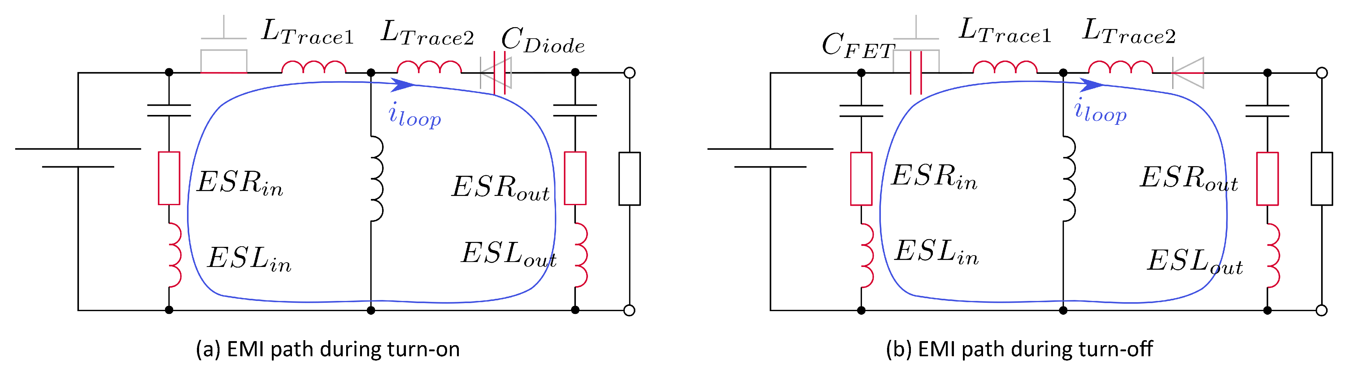
3.1. EMI Path When the Switch Is Closed
Turning on MOSFET increases the phase voltage and reverses the bias of the diode. The fast transient excites an LC structure that is formed by the loop inductance and the diode capacitance (blue line in
Figure 3a). Interestingly, the main inductor was not part of this path as long as we could neglect its parasitic parallel capacitance.
3.2. EMI Path When the Switch Is Open
The resonance circuit is different during turn-off; see
Figure 3b. Two aspects determine the differences between turn-on and turn-off ringing:
The inductances stay the same, but the critical capacitance changes from the diode to the MOSFET. Both are nonlinear.
The voltage rise, and fall times are usually not the same, leading to different excitations of the resonances.
4. Simulation Model in Different Levels
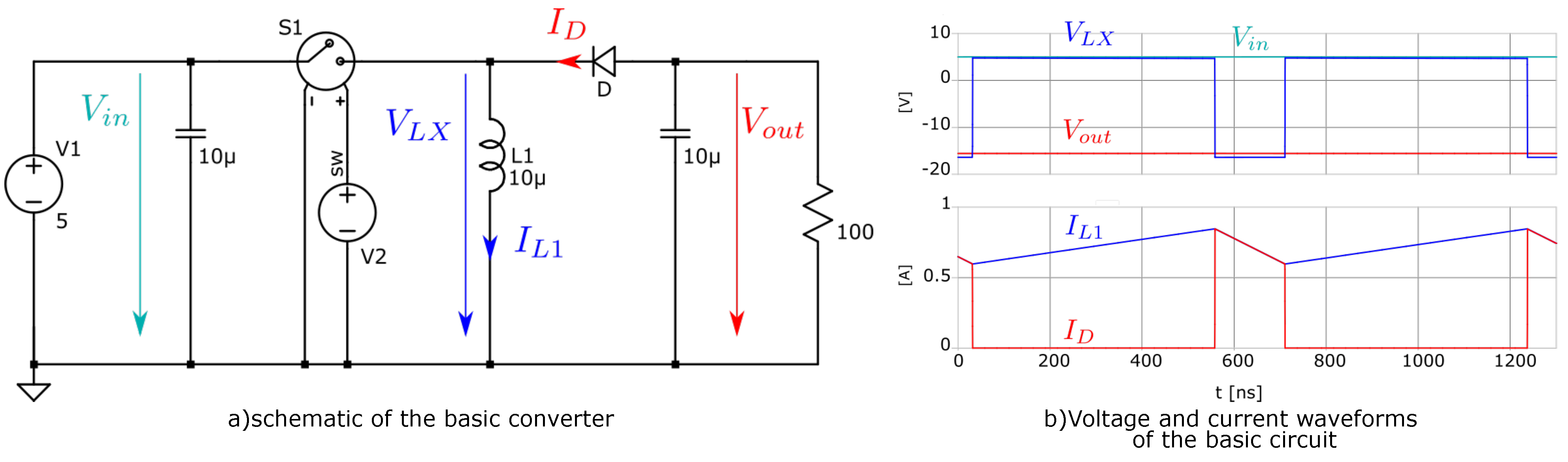
We first present a basic SPICE circuit in
Figure 4 to familiarize the reader with the basic function. This is later extended to include parasitic components to illustrate the EMI behavior.
4.1. Basic Simulation Model
Figure 4 shows taht the transistor and controller IC were replaced with an ideal SPICE switch driven by a pulse voltage source. As all the components and the connections were ideal, no parasitic resonances or overshoots occurred during simulation. The simulation results and the schematic shown in
Figure 4 demonstrate the basic switching action.
4.2. Simulation Model including Parasitics
Figure 5 shows the extended model. A 100
capacitor was added in parallel with the switch to simulate the drain–source capacitance of a MOSFET. A fixed switch capacitance was used for the sake of simplicity. In
Section 5.2, a model of a PMOS transistor was used. In addition, a real model of a Schottky diode (SL03), a parasitic capacitance of the inductor, ESL and ESR of the capacitors, and trace impedances were added. The extended simulation model is shown in
Figure 5.
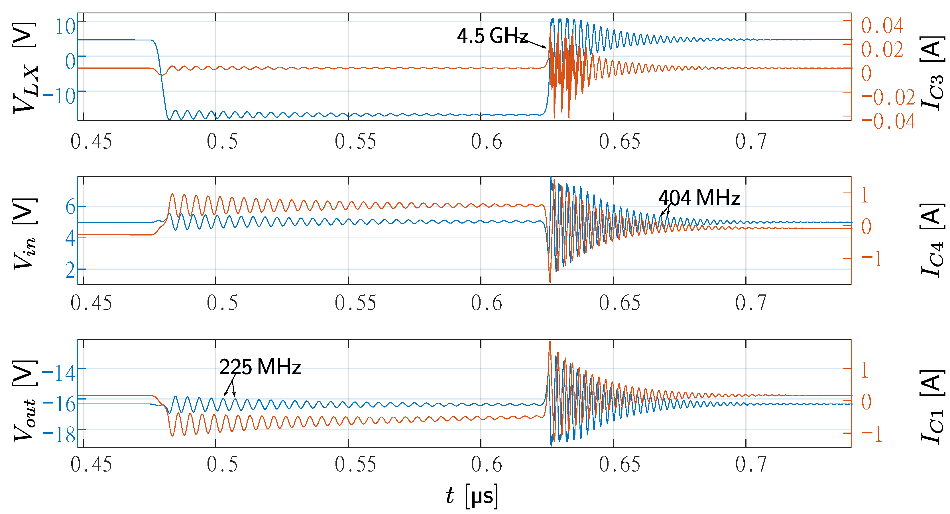
During turn-on, the dominating resonance is formed by the capacitance of the diode and the loop inductance
of the circuit, which is the sum of
,
and the ESL of the in- and output capacitors. The frequency can be calculated with (
1). The simulation results during turn-on and turn-off are presented in
Figure 6.
During turn-off, the dominating resonance is formed by the capacitance of the switch and the loop inductance. The frequency can be calculated with (
2).
During turn-on, another resonance is formed by the capacitance of the inductor and the loop inductance
, which is formed by
. The frequency of this resonance is calculated in (
3). This resonance is also visible in
Figure 6.
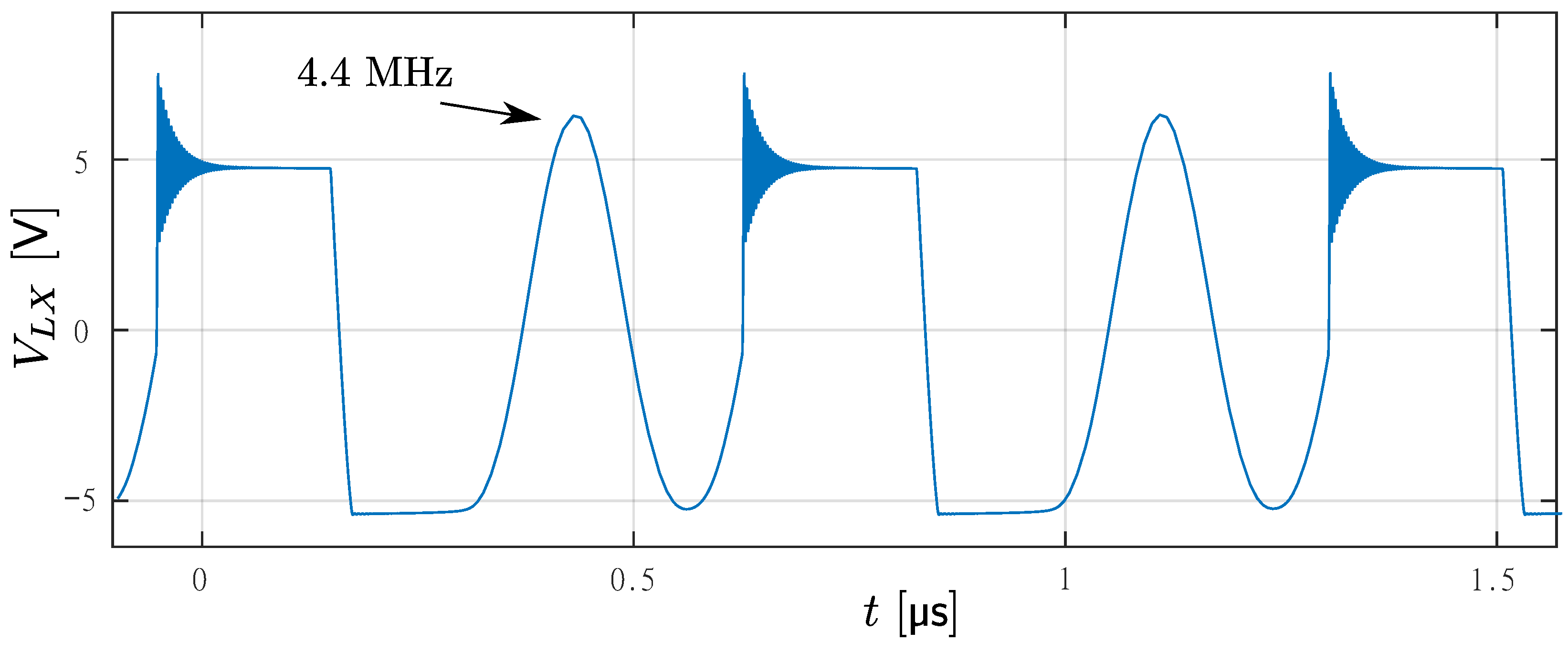
This is the highest frequency in the circuit. The lowest frequency resonance in the circuit was found during the discontinuous conduction mode (
Figure 7). As no DC current was flowing through the main inductor, the transistor and the diode acted like capacitors. The main inductor was then part of the resonances. Interestingly, the highest and the lowest frequency resonances were formed by the same loops, but all inductors were transformed into inductors and vice versa. The resonance frequency in the discontinuous current mode is calculated in (
4).
The EMI voltage on the input and output ports could be calculated with (
5), where ESL and ESR are the parasitics of the in- or output capacitor,
is the current in the high-frequency loop, and
the angular frequency of the current.
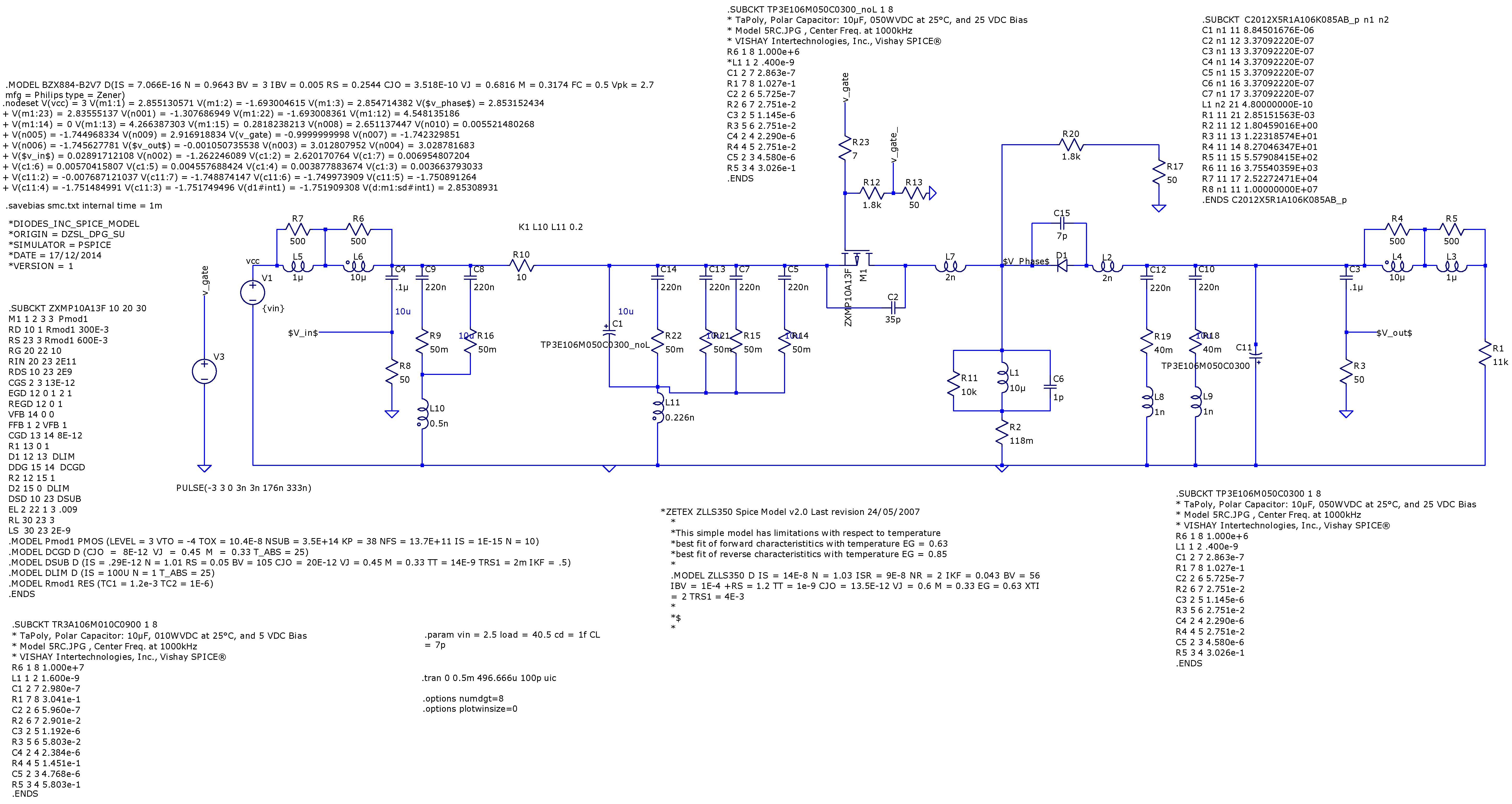
5. Converter Built with Discrete Components
To confirm the correctness of the observations obtained by simulation, a converter was built from discrete components, and measurements were taken. The SPICE model was adapted to the components used in the circuit. The SPICE simulation model can be found in
Appendix A. The structure of the converter was kept as simple as possible without any control loop to control the output voltage. The assembly used a minimal area (50
× 30
) on a solid ground plane.
Since the aim of this article was to illustrate dominating EMI generation processes, a very fast gate driver was selected. The 20% to 80% rise time of the gate driver was , and the slew rate during the rising edge was /. The 80% to 20% fall time was . The slew rate during falling was /. The output of the gate driver increased from −3 to 3 . The source of the MOSFET was connected to the input port , so the gate-source voltage rises from −6 to 0 .
To avoid bootstrapping, a P-channel MOSFET was used. For both the diode and the MOSFET, low-capacitance devices were selected to increase the values. The resulting 20% to 80% slew rate on the phase node was / during the rising edge, and / during the falling edge.
A list of the used components is shown in
Table 1.
To illustrate the EMI behavior and compare it with the simulation, additional discrete capacitors were added to vary the diode and MOSFET capacitances in both the simulation and the measurements. Further, inductances were added to observe the resonances when the loop inductance was varied.
5.1. Measurement of the Converter
Figure 8 shows the principal measurement setup, which was realized on a solid ground plane. The EMI currents could be captured using
bandwith Line Impedance Stabilization Networks (LISNs) placed on the input and output. LISNs prevented the high-frequency signals from reaching the source and load. Instead, radio frequency (RF) currents were redirected into the 50
port of the measurement device.
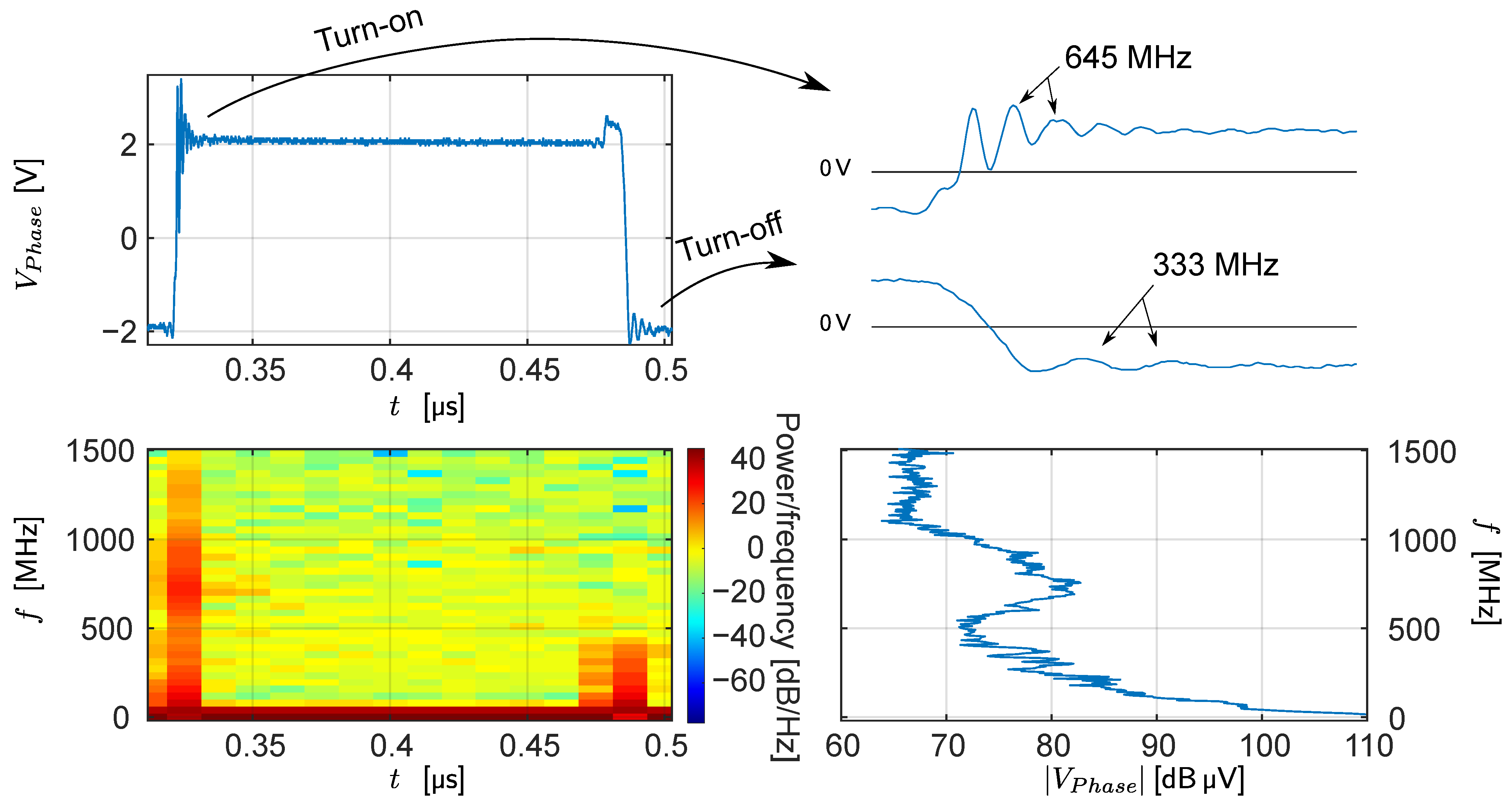
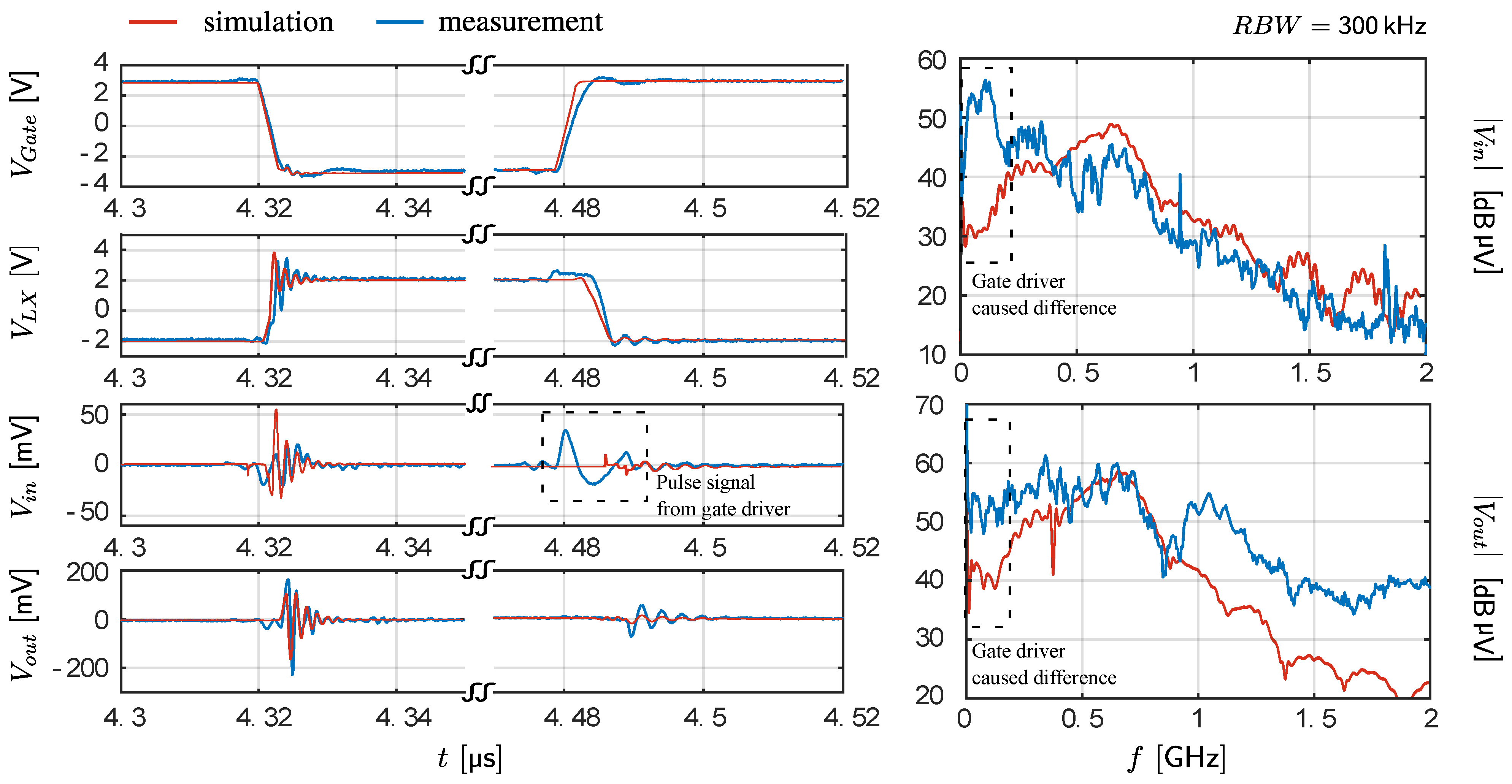
The phase voltage was probed via terminating into a 50 oscilloscope input. We did not attempt to measure the current, as the introduction of any current probe would add at least a few into the loop. The measurements were taken with an oscilloscope and a spectral analyzer on ports ,, and . A 50 coax cable was directly connected to the nodes to be measured on the PCB. The oscilloscope had 4 channels, which allowed for capturing time domain signals on the ports at the same time. The 4 input bandwidth of the oscilloscope allowed for zooming into the ringing, and measuring the ringing frequency during turn-on and turn-off events. The used spectral analyzer had only one channel, so the frequency domain measurements were taken sequentially. The reslolution bandwidth (RBW) of the spectral analyzer was set to 300 for all frequency domain measurements. The gate driver had a positive and a negative supply voltage. The negative supply voltage was fixed to , and the positive was connected to the input voltage of the converter to guarantee that the transistor was in a completely off state. The gate-source voltage of the MOSFET thus changes from 0 to −6 . The PWM signal which controls the gate driver is set to a duty cycle and a frequency of 3 .
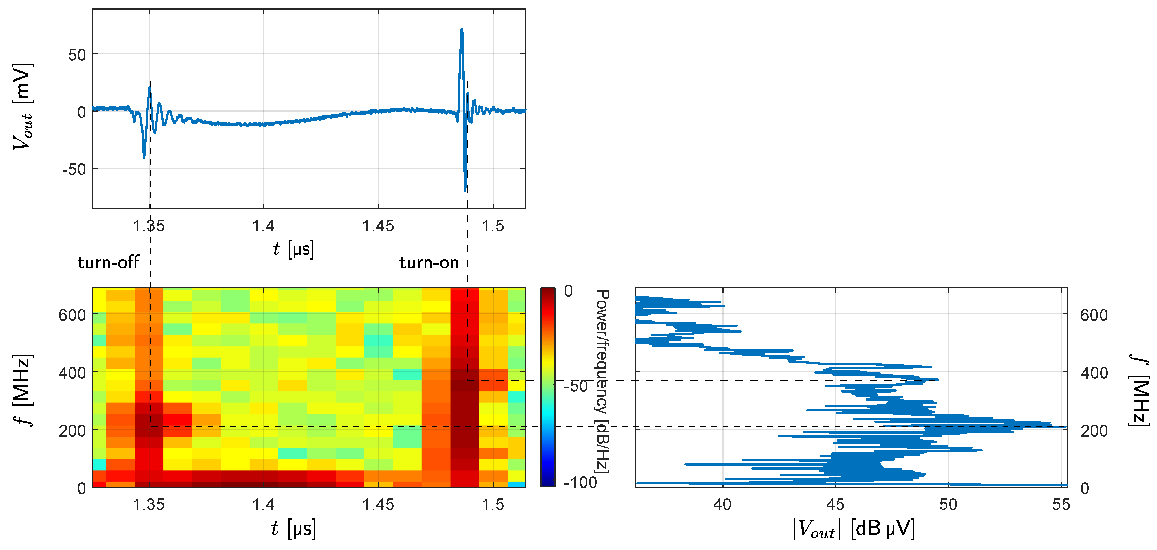
Figure 9 shows the measurement results on the phase node of the converter. The time-domain signal, the frequency spectrum, and the spectrogram of the signal are shown. The difference in oscillation frequency in turn-on and turn-off is visible. The dominant frequencies are also visible in the time domain data, 333
during the turn-off event and 645
during the turn-on event. Both frequencies were visible as peaks in the frequency spectrum.
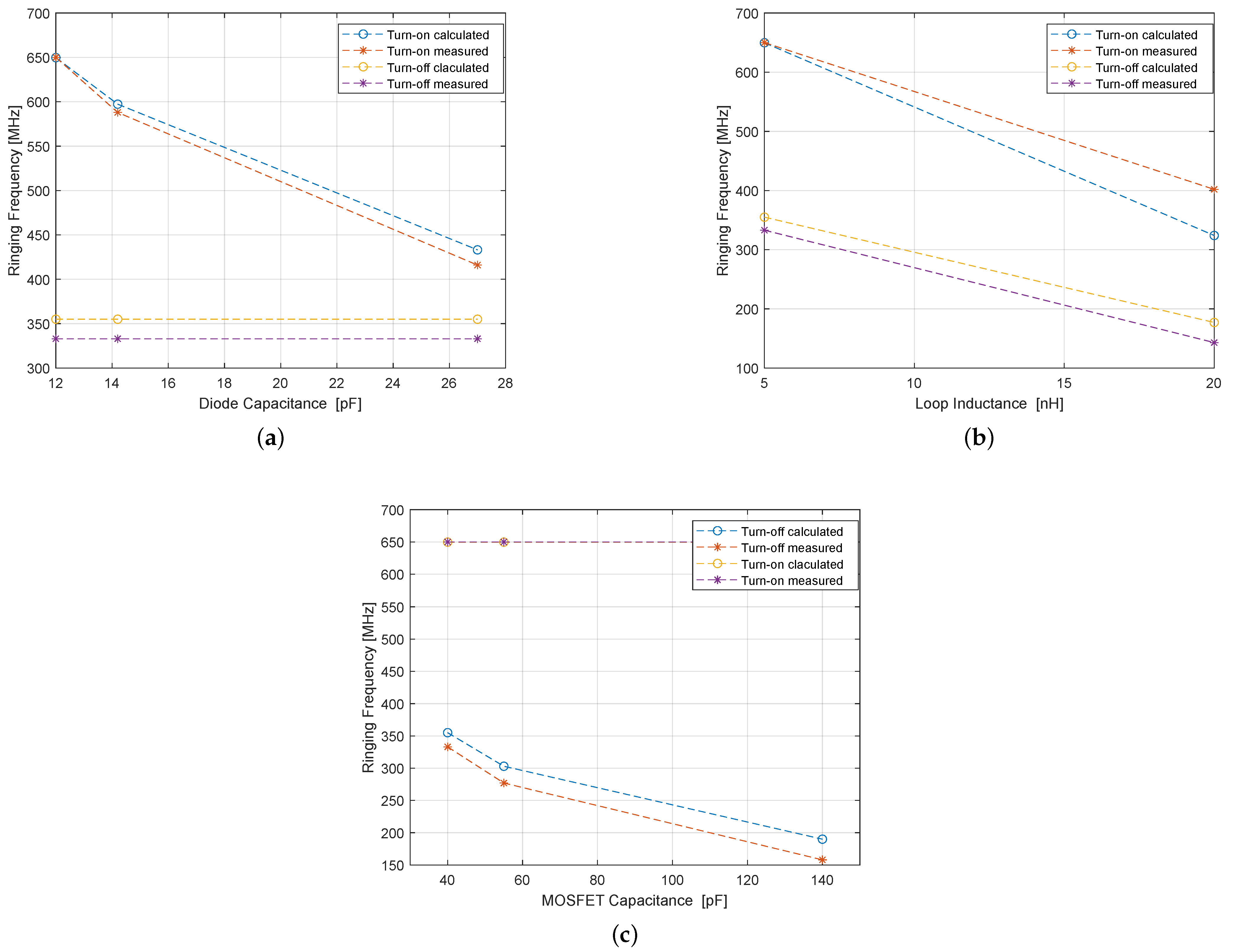
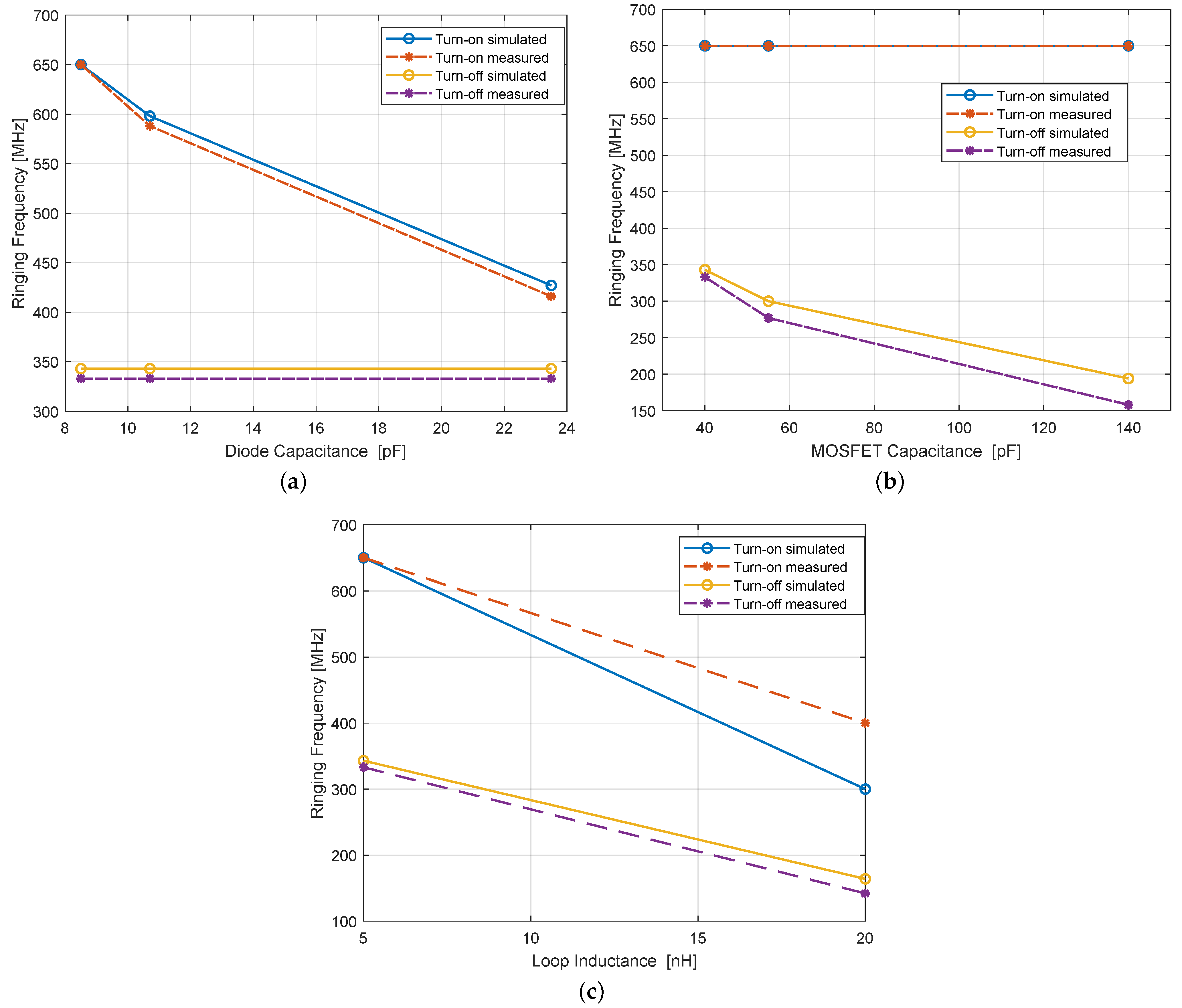
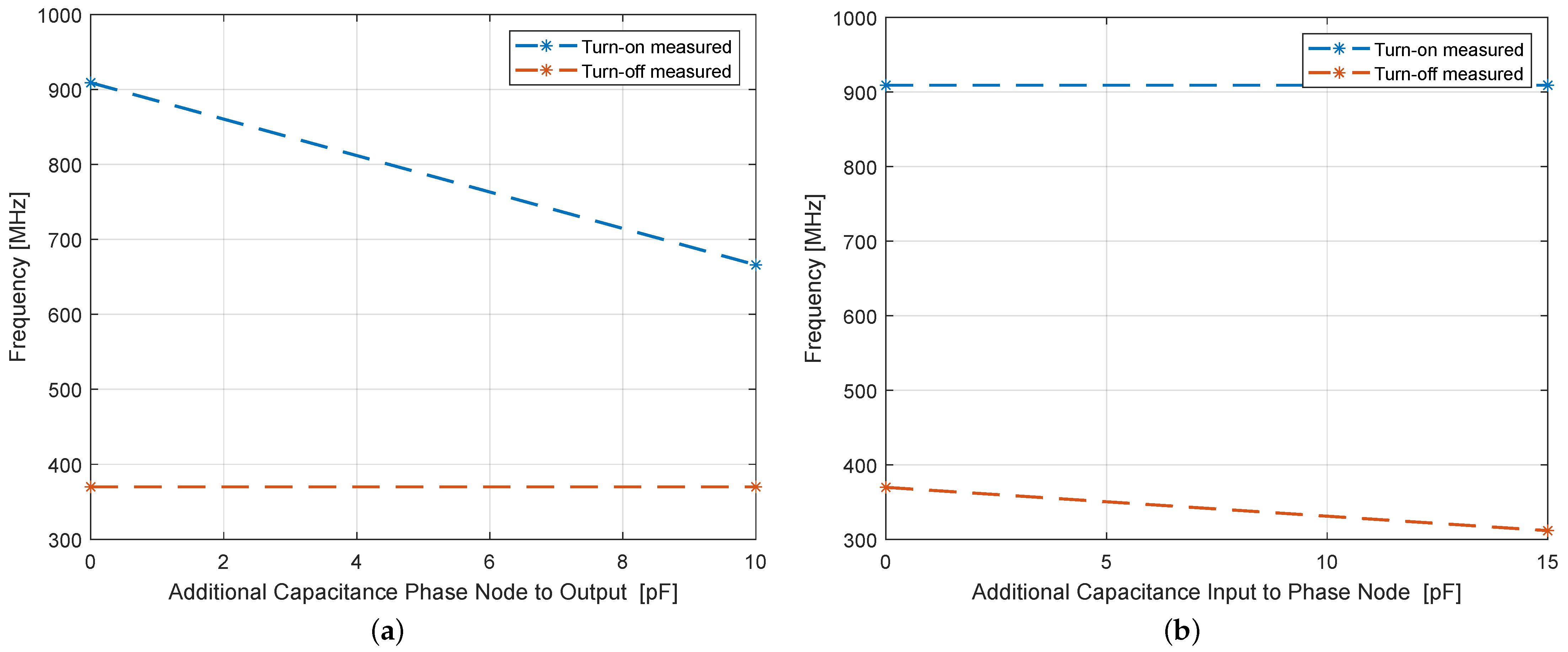
To provide evidence for the analysis of the two main loops causing EMI, capacitors were placed in parallel with the diode and/or the MOSFET. By adding different capacitors in parallel with the diode, the influence of the diode capacitance was investigated.
Figure 10 compares the oscillation frequencies with different values of the circuit parasitics. Using (
1) and (
2), including the resulting diode capacitance due to the parallel connection, led to the calculated data in
Figure 10. The oscillation frequencies during the turn-on event were decreased, while the frequencies during turn-off were approximately the same. This confirms the EMI path discussed in
Section 3.1 and the analysis of the resonance during the turn-on given in
Section 4.2.
The influence of the loop inductance was investigated by adding a 15
inductor in series to the diode. Due to the increased loop inductance, both EMI paths were affected, and both parasitic resonances were shifted to lower frequencies; see
Figure 10. The calculated results in that figure were again obtained with (
1) and (
2) using the resulting loop inductance.
The influence of the MOSFET capacitance could be observed by adding different capacitor values across the drain and source of the transistor.
Figure 10 compares the different oscillation frequencies with different capacitor values. The calculated values were obtained using (
1) and (
2) using the resulting MOSFET capacitance. A decrease in the ringing frequency during turn-off with increasing capacitor values is visible. The frequency during turn-on stayed constant, confirming the analysis of
Section 4.2 and the EMI path discussed in
Section 3.2.
5.2. Simulation of the Converter
The SPICE simulation model was adapted to the used components and the estimated parasitics of the PCB. SPICE models of the transistor and the diode were provided by the manufacturer.
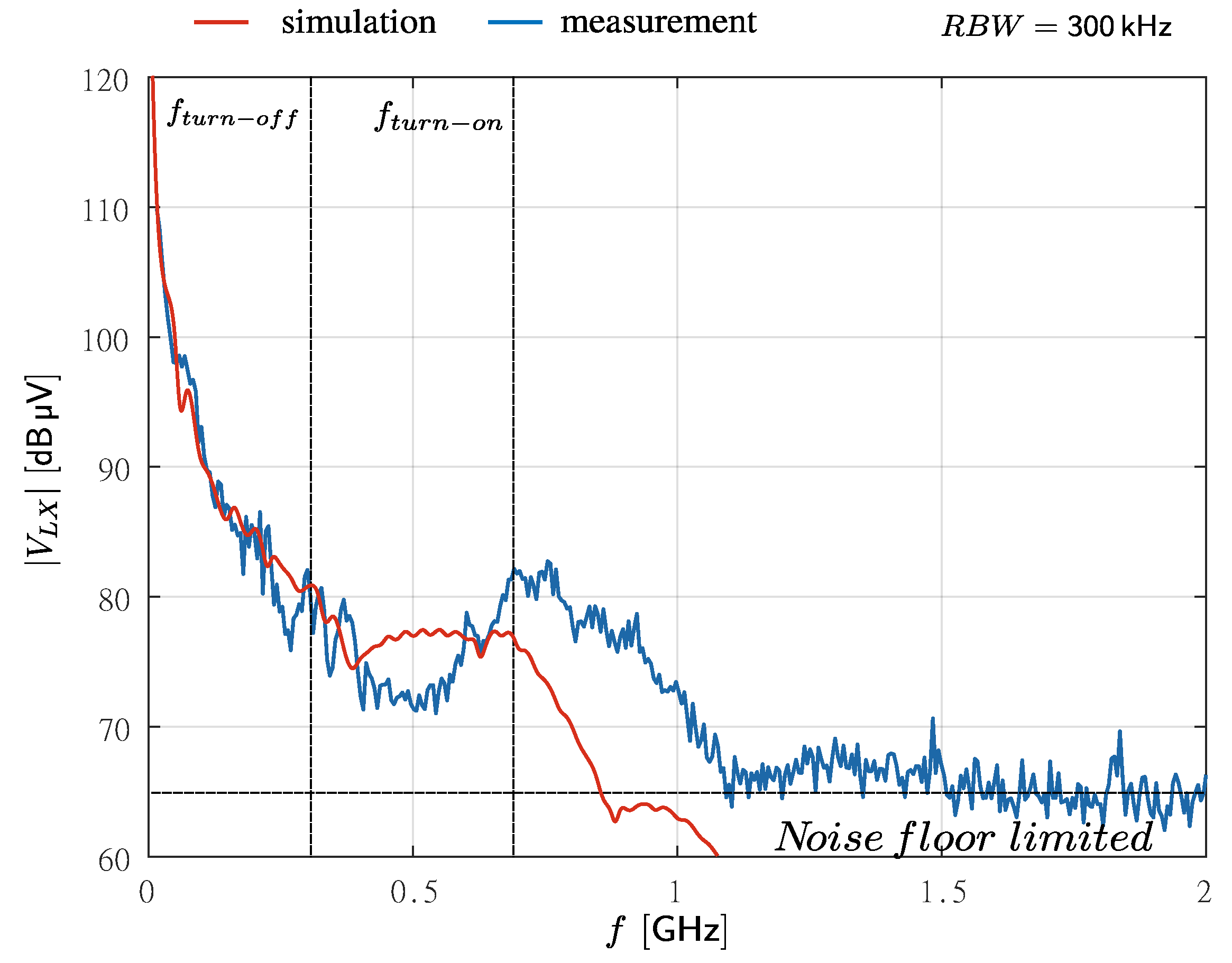
Figure 11 shows the simulation results compared to the measurements on the phase node of the converter. A spike at 650
is visible in the simulation and measurement results. The spike corresponds to the turn-on ringing. The turn-off frequency is not visible in the simulation because of the small amplitude of the ringing and the high low-frequency components in the signal.
The frequency spectra of the in- and output ports, and the time domain signals are shown in
Figure 12. The spectra of the in- and output show two peaks on the turn-on (333
) and turn-off (645
). The simulation results show slightly higher frequencies. The simulated and the measured signals correspond in the time domain. A pre-pulse is visible on the input port, before turn-on and turn-off. This pre-pulse is generated by the gate driver, which is not modeled adequately in the simulation model. This pre-pulse is also observed when the input voltage of the converter is set to 0
and no current flows from the input into the converter circuit. The frequency range above 1
is not well modeled. This is why the measurement results and the simulation results differ in this area.
We did similar experiments in simulation as we did in measurements. The capacitances across the transistor and diode, and the loop inductance are varied to compare the change in behavior in simulation and measurement.
The main effects observed during the measurement are also visible in the simulation. By increasing the capacitance across the diode, the frequency of the turn-on ringing is shifted to lower frequency values. The results are shown in
Figure 13.
By increasing the capacitance across the transistor, the ringing frequency during the turn-off event was shifted to lower frequencies. The simulation results are shown in
Figure 13.
Increasing the loop inductance affected the ringing frequency during both turn-on and turn-off. Both frequencies were shifted to lower frequency values. The results are shown in
Figure 13.
The discussed simulations again confirmed the EMI paths derived in
Section 3.
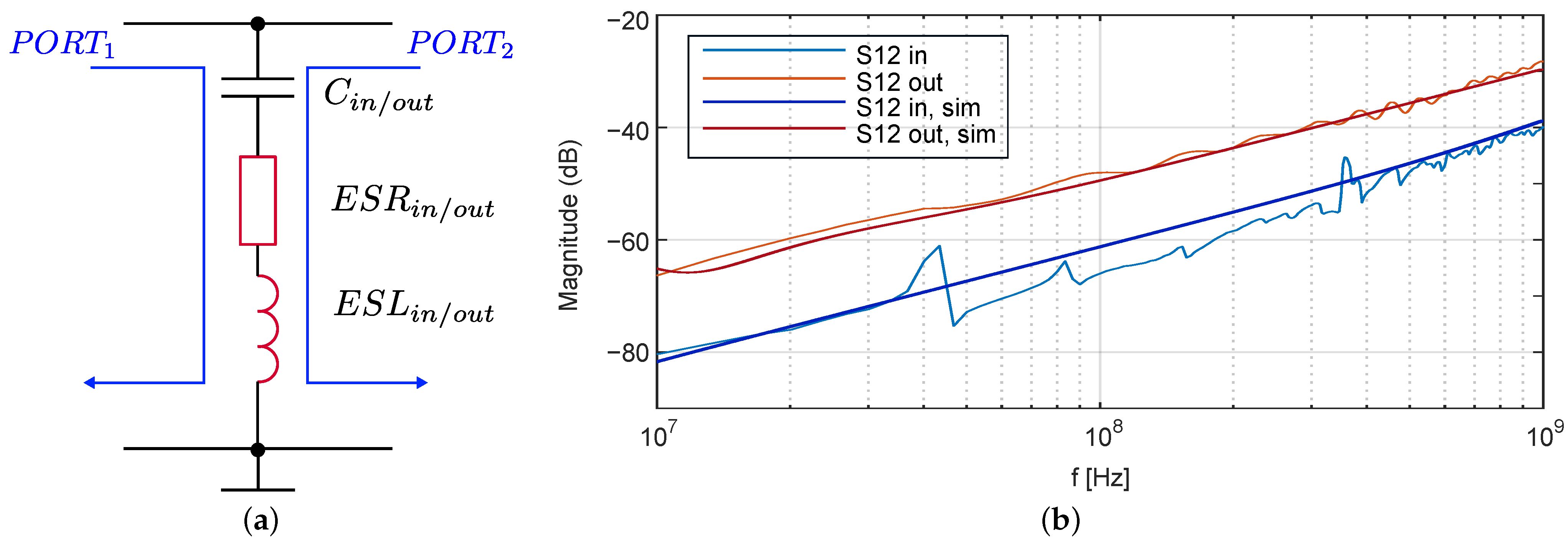
The EMI current could be estimated using the measured EMI voltage on the phase node and the parasitics along the EMI path. The parasitic capacitances of diode (
) and transistor (
) are given in the datasheet. The ESL of the input and output capacitors was measured by measuring the S12 parameter. The measurement setup is shown in
Figure 14. The setup was the same for measuring the input and output capacitors. The capacitor was connected to the ground, and the S12 was measured from Port 1 to Port 2. The results of these measurements are shown in
Figure 14. Since we wanted to estimate the ESL of the capacitors, the plot shows the S12 in the frequency range where the capacitor showed its inductive behavior. The ESL of the input capacitors was approximately 50
, and the ESL of the output capacitors was approximately 400
. Several capacitors were connected in parallel at the input and the output. So, the measured ESL must be understood as the effective ESL of the capacitors in parallel. There was a significant difference between the ESL values at the input and the output because more capacitors were connected in parallel at the input.
Inductances
and
were estimated using the measured ringing frequencies and the known parasitics of the electronic components. The resonance frequency during turn-on is given with (
1).
is the sum of
,
, and the ESL of the in- and output capacitors. With this information,
and
could be estimated to approximately 2
.
The simple simulation model shows the basic behavior and function of an inverting buck/boost converter. The model including the parasitics of the circuit could reconstruct the fundamental resonances that occur when turning MOSFET on and off. The measurements on the circuit, designed with discrete components, confirm the explored theories by means of simulation. The influence of the MOSFET capacitance during turn-on, and of the diode capacitance during turn-off was confirmed with a modification of the tested circuit in terms of adding capacitors in parallel with the diode and the MOSFET.
6. Measurements on Commercial Converters
To verify the EMI analysis on actual circuits, different commercially available converters were investigated. In principle, these converters showed similar behavior. However, due to the fact that the internal structure of the converters was not known, only assumptions could be made about their internal behavior.
Two different evaluation boards were investigated. The two converters had the same nonisolated inverting buck/boost topology. They differed in switching frequency, gate drive, input voltage range, output voltage, and maximal output current. The specifications of the different evaluation boards are listed in
Table 2 6.1. Measurement Setup
The ground plane of the evaluation board was soldered directly onto a large copper reference plane in order to achieve a similar measurement setup to that shown in
Figure 8.
bandwidth LISNs was added to the circuit.
6.2. Measurement Results of the Commercial Converters
Measurements on the commercial converters showed similar behavior to that of measurements on the converter built with discrete components. Different ringing frequencies during turn-on and turn-off could be observed. Frequencies during turn-on were significantly higher than those during turn-off, indicating low diode capacitance.
Figure 15 shows the influence of the diode capacitance on the ringing frequencies.
The influence of the parasitic capacitance of the transistor is shown in
Figure 15. For these measurements, an additional capacitor was connected in parallel with the input and the phase node. As the exact internal structure of the converter was not known, and the additional capacitance may have also influenced other operations in the converter, the measured results may not describe the influence of the MOSFET capacitance exactly. However, as expected, the ringing frequency during turn-off was lowered by the additional capacitance across the input and the phase node.
ADP5075 allows for changing its phase node slew rate. The voltage slew rate changes from 2.7 / to 5.7 / during turn-on and from −1.8 / to −3.3 / during turn-off.
In addition to the frequency measurements, we also measured the efficiency. With lower slew rates, the EMI amplitude of the converter decreased in the frequency region from 400
to
(
Figure 16).
The second commercial converter, TPS63700, showed similar behavior, indicating that SPICE-based analysis and the converter designed from discrete components captured the main EMI properties of this class of converters.
As with the other converters examined in this paper, two different resonances could be observed. The resonance frequency during turn-on (368
) was higher than the resonance frequency during turn-off (215
).
Figure 17 shows the spectrogram and the time domain signal on the output port of the converter.
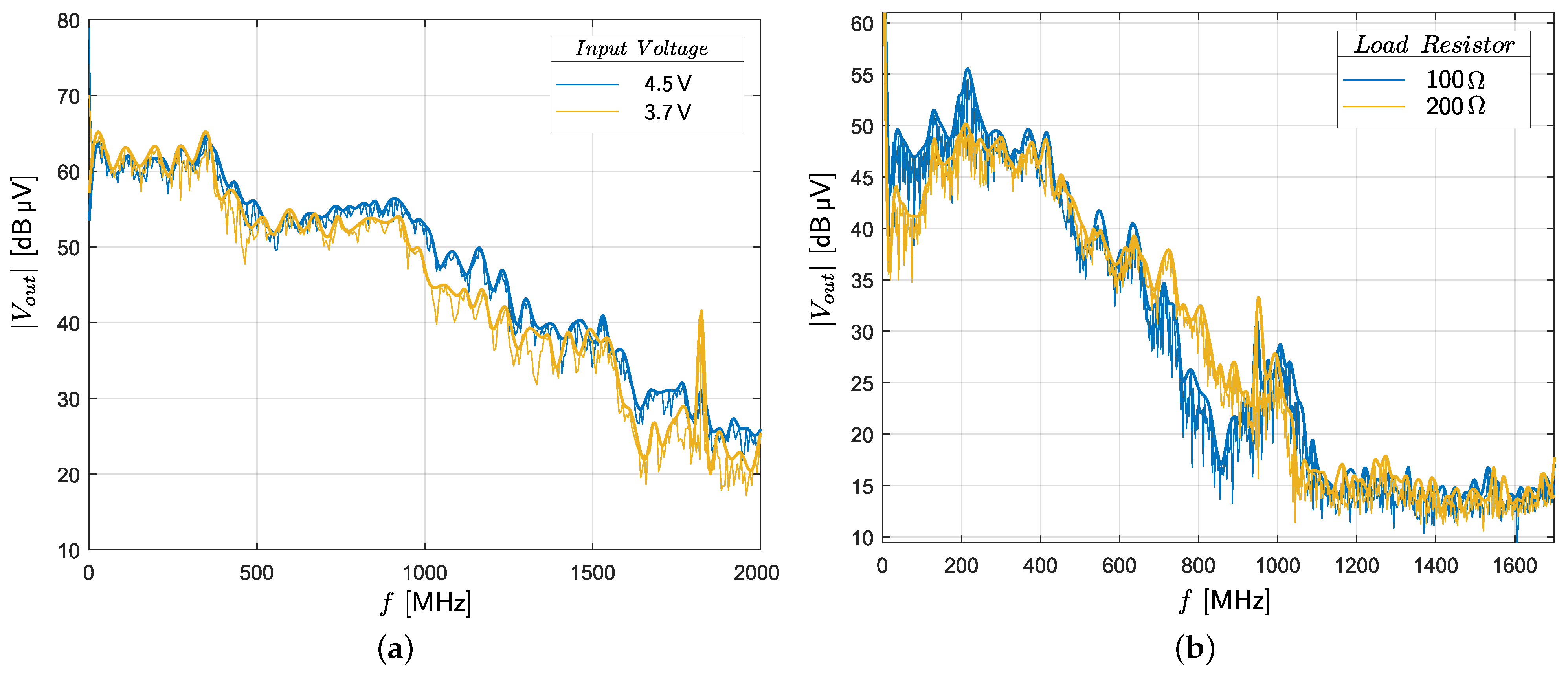
Figure 18 shows the frequency spectrum of ADP5075 on the output port depending on the input voltage. The amplitude of the 909
turn-on ringing was increased with a higher input voltage. Due to the increased input voltage, the amplitude of the phase node voltage and the slew rate increased. The turn-off ringing amplitude remained unchanged while the input voltage was varied because of the internal regulation of the output voltage.
Figure 18 shows the frequency spectrum of TPS63700 on the output port. The 215
turn-off ringing amplitude was decreased by higher load resistors. This can be explained by the decreased load current. So, the current that discharged the phase node capacitance during turn-off was smaller; therefore, the voltage slew rate on the phase node was decreased during turn-off. Due to the internal control loop, the output voltage was kept constant while varying the load resistor. So, the turn-on transition was nearly unchanged.
Table 3 shows a comparison of the ringing frequencies of the investigated converters.
7. Conclusions
The EMC analysis of the inverting buck/boost converter showed that two resonances were excited, and both the input and the output sides of the converter could conduct EMI signals. One resonance was excited during turn-on, and the other during turn-off. In both cases, the inductance was formed by the loop inductance that included the capacitor, the MOSFET, the diode and the decoupling capacitors. For turn-on, however, the reversed biased diode formed the capacitor, while after turn-off, the MOSFET formed the capacitance, and the diode conducted currents. This general behavior was verified in simulation and with the design of a converter from discrete components. The analysis of commercial converters demonstrated the same behavior in principle, even though the internal structure of commercial converters is not known.


