1. Introduction
In the last few decades, there has been an increasingly profound influence of various digital systems on all aspects of human activity [
1]. This applies primarily to personal computers, embedded systems, the Internet, and the Internet of Things [
2]. All such systems are built using ultra-large integrated circuits such as ASICs and field-programmable gate arrays (FPGAs) [
3]. Such chips are extremely complex: currently, they include 7–8 billion transistors [
3]. This causes an urgent need to develop efficient computer-aided design (CAD) methods for implementing digital systems based on such chips. In the case of FPGA-based systems, technological mapping [
4] is performed by industrial CAD systems of firms manufacturing particular chips such as Intel (Altera) or AMD (Xilinx: San Jose, California, U.S. ) [
5,
6]. These industrial CADs include a limited number of synthesis methods. However, it is possible to use them together with some external synthesis methods, where the original structural diagrams of FSM circuits are represented by HDL models [
7]. Our current article is aimed at working out an FSM design method improving the characteristics of sequential blocks of FPGA-based digital systems. The step of synthesis is executed by our program tools, whereas the step of technology mapping is executed by the industrial CAD tool Vivado [
8] by AMD (Xilinx).
One of the fundamental models used for representing sequential devices is the model of the Mealy finite state machine (FSM) [
4]. In this paper, we discuss a case when FSM circuits are implemented using the internal resources of FPGAs [
9]. The choice of these particular VLSI chips is determined by the fact that, now, a huge number of various projects are implemented using FPGAs [
10]. Furthermore, it is clear that FPGAs will dominate logic design in the next few decades [
7].
During the design process of FSM circuits, some optimization problems arise. As a rule, they are the following: minimizing the chip area occupied by an FSM circuit; reducing the value of the FSM cycle time (maximizing the operating frequency); minimizing the power consumption [
11].
A digital system may include a number of sequential blocks [
1]. The behavior of any sequential block, consisting of a combinational part and memory, can be represented using the FSM model. For each digital system, the ratio between the total complexity of processor units and memory units, on the one hand, and various FSMs, on the other hand, depends on the features of the system. The larger the proportion of the FSM-based part, the more important is the reduction in the chip area occupied by the circuits of each FSM. Solving this problem can lead to several positive effects [
2]. Firstly, it can allow expanding the functionality of the whole system by expanding the functionality of the processor and other units of the system (since, after optimization of the FSM circuits, additional area will appear). Secondly, it may be possible to implement the system using less-powerful FPGA chips. Thirdly, a reduction in the area of the circuit leads to a decrease in power consumption, which is especially important for autonomous and mobile systems. In all these cases, the competitiveness of the designed digital system in relation to similar concurrent projects increases. All of the above shows the importance and necessity of optimizing the circuits of FSMs that are part of digital systems. Obviously, this area reduction is expedient as long as the performance of the optimized block remains within the specified limits [
2].
In this paper, we discuss the case when FSM circuits are implemented using look-up table (LUT) elements [
12]. The following internal resources are used for implementing FSM circuits: LUTs, flip-flops, synchronization tree, dedicated multiplexers, programmable interconnections, and input–outputs [
12]. If an FSM circuit is implemented with these resources, then the occupied chip area is estimated as the number of LUTs (LUT count) [
13]. As shown in [
11], the reduction of the LUT count also reduces the power consumption. However, the area reduction can degrade the FSM’s performance [
14]. This degradation is an overhead of area reduction. In this paper, we propose a method that leads to simultaneously reducing the area with a slight increase in the FSM maximum operating frequency (compared to equivalent FSM circuits based on encoding of collections of outputs (COs) [
11].
The main scientific novelty of our article is associated with the development of a new type of state code, called two-part codes. The first part contains the code for some class of the set of FSM states. The second part contains the code of state as an element of this class. Such an approach allows simultaneously reducing the number of LUTs in the FSM circuit and increasing its performance.
The main contribution of this paper is a novel method improving both the LUT counts and the performance of the FPGA-based circuits of Mealy FSMs. The improvement is associated with reducing the number of literals in Boolean functions representing an FSM circuit. A further decrease in the number of elements is associated with the proposed modification of the method of unitary-binary maximum encoding of output collections. This modification allows using the resources of a single LUT to generate two outputs. The proposed method belongs to the methods of structural decomposition [
11]. The results of the experiments showed that the proposed approach improves two characteristics of FSM circuits (LUT count and maximum operating frequency) as compared to the FSM circuits based on the maximum binary encoding of both states and collections of outputs [
11].
The rest of the paper is organized as follows.
Section 2 includes the basic information connected with the LUT-based Mealy FSM design. The state-of-the-art is analyzed in
Section 3.
Section 4 shows the main idea of the proposed approach. We show a synthesis example based on the proposed method in
Section 5. The experimental results conducted with standard benchmarks are analyzed in
Section 6. Finally, the article ends with a short conclusion.
In the further text, we use many notations. To facilitate understanding of the proposed method, we placed the main notation in
Table 1.
2. Basics of Mealy FSM Design with LUTs
In many cases, either a state transition graph (STG) or a state transition table (STT) is used to represent the behavior of the Mealy FSM [
15]. Using these forms, the three following sets can be derived: a set of states
, a set of inputs
, and a set of outputs
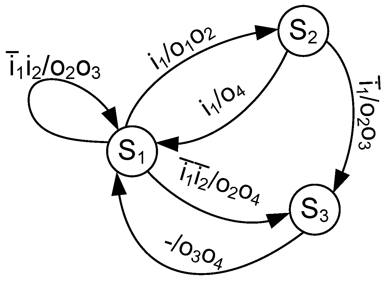
. Therefore, an FSM has G states, U inputs, and W outputs. In the case of STG, its vertices correspond to states, and arcs correspond to interstate transitions. Above each arc, there are written FSM inputs causing a particular transition and outputs associated with this transition [
15]. An STT represents an STG as a list of transitions, where each line corresponds to a particular transition. Therefore, if there are H arcs in an STG, then there are H lines in a corresponding STT. For example, some FSM
is represented by an STG shown in
Figure 1.
FSM Ex1 is characterized by sets
,
, and
. Therefore, there are G = 3, U = 2, and W = 4. There are H = 6 arcs in this graph. Each arc is represented by a single line of
Table 2.
The transformation of the STG (
Figure 1) into the STT (
Table 2) is executed in a trivial way. Obviously, it is possible to transform any STT into the corresponding STG.
To design an FSM circuit, each state
is represented by a binary code
. This is performed during the step of state assignment [
15]. In the case of maximum binary (MB) state assignment, state codes consist of
bits:
Formula (
1) determines a minimum possible number of state variables.
In a common case, the states are encoded using state variables from the set
. Each bit of
corresponds to a flip-flop. These flip-flops are combined into a code state register (RG). Very often, the RG consists of D flip-flops [
4].
The maximum number of state code bits
is used in the case of one-hot
state assignment. The value of
is determined as
The flip-flops are controlled by input memory functions (IMFs), a pulse of initialization , and a pulse of synchronization . The IMFs form a set . The value of R depends on the state assignment method used. It could be either or or some intermediate value. To load a code of the initial state into the RG, the pulse is used. The IMFs determine a code of the next state. This code is loaded into the RG using the pulse .
A Mealy FSM logic circuit consists of a combinational part and memory [
4]. The memory is represented by the RG. The combinational part is represented by the following systems of Boolean functions (SBFs) [
15]:
The systems (
3) and (
4) determine a structural diagram of Mealy FSM
(
Figure 2).
The combinational part (
Figure 2) implements SBFs (
3) and (
4). It is represented by a network of particular logic elements. The FSM memory is the register RG. The RG includes R master–slave flip-flops controlled by pulses
and
.
The SBFs (
3) and (
4) are constructed using an FSM direct structure table (DST) [
2]. To create a DST, it is convenient to transform the initial STG into the STT. An STT includes five columns [
16]. A current state is shown in a column CS; a column ST includes a state of transition; an input signal
is shown in a column In; a column Out includes a collection of outputs (CO)
; h is a number of interstate transitions (
). The transformation of an STG into an equivalent STT is executed in a trivial way [
16]. A DST includes all columns of a particular STT and three additional columns [
15]. These additional columns are [
16]: codes of the current state and the state of transition and the symbols of IMFs equal to 1 to load the next code into the RG.
The design method depends significantly on the properties of the logic elements used. In the case of LUT-based FSMs, an FSM circuit is implemented as a network of configurable logic blocks (CLBs). Each CLB includes LUTs, programmable flip-flops, and dedicated multiplexers. The resulting network is created using a programmable routing matrix [
3]. Our paper targets FPGAs produced by Xilinx [
12]. A peculiarity of their CLBs is the reconfigurability of the LUTs: the number of LUT inputs can be changed using dedicated multiplexers. There is some basic LUT having
inputs. Using multiplexers allows creating LUTs having either 7 or 8 inputs. These resulting LUTs have approximately the same performance as the basic LUTs [
17].
The second peculiarity of AMD Xilinx FPGAs is the ability to share the resources of the basic LUT to implement two functions that depend on the same arguments. Therefore, a basic LUT is “split” by two LUTs having inputs. We denote these two LUTs as a shared LUT (SLUT).
In the LUT-based FSMs, the RG is distributed among flip-flops of CLBs implementing SBF (
3). Therefore, the RG is hidden inside the CLBs. This gives the structural diagram of LUT-based Mealy FSM
shown in
Figure 3.
A block CPSV includes the hidden distributed register RG. The pulses
and
control the operation of the RG. The LUTs of CPSV generate IMFs (
3) entering the informational inputs of D flip-flops. As a result, the state variables
are generated. The block CPO generates outputs
represented by (
4).
Each Boolean function
depends on
arguments (
). Our analysis shows that for some FSMs from the library [
18], the value of
is around 20. However the number of LUT inputs (
) is very small [
3]. Therefore, the following condition can take place:
If the condition (
5) holds, then some serious problems can arise [
4,
11]. First of all, there is more than a single LUT in a circuit corresponding to a function that satisfies the condition (
5). This increases both the number of logic levels and the number of interconnections inside this circuit. In turn, this increases both the propagation time and consumed power compared to an equivalent single-level circuit. Therefore, the fulfillment of the condition (
5) has a significant negative effect on the quality of the LUT-based FSM circuit.
3. Related Works
If the condition (
5) holds for some function, then the various methods of functional decomposition (FD) [
4] are used for executing the step of technology mapping for a corresponding circuit. The decomposed function
is represented by a composition of partial functions. The logic circuit for each partial function includes only a single LUT. These LUTs are connected to create a final circuit.
The methods of functional decomposition are discussed in many books and papers, for example in [
4,
14,
19,
20,
21,
22]. The FD is a very powerful tool used in the process of technology mapping [
4]. If the condition (
5) holds, then such a function is broken down into smaller and smaller components. The decomposition is terminated when each component is represented by an SOP having no more than
arguments. The main drawback of FD-based FSM design is the multi-level nature of the produced circuits. In multi-level circuits, it is quite possible that the same inputs
appear on several logic levels. This results in FSM circuits with “spaghetti-type” interconnections.
If the condition (
5) is violated, then there are exactly
LUTs in an FSM circuit. Otherwise, an FSM circuit is represented by
functions, where
is a set of partial functions obtained in the process of decomposition. The partial functions are components of functions
.
The negative effects of FD-based FSM circuits are well known [
11]. They are connected with “spaghetti-type” interconnections typical for such circuits. For modern nanoelectronics, as mentioned in [
23], “…wire delay has come to dominate logic delay”. Therefore, FD-based FSM circuits are much slower than their single-level counterparts. Furthermore, the interconnections are responsible for up to 70% of total power consumption [
23]. Due to this, the FD-based FSM circuits consume more power than their single-level counterparts.
To improve the characteristics of FSM circuits, the interconnection system should be improved. This can be performed, for example, by reducing the number of literals in the sum-of-products (SOPs) representing functions
. This reducing can be achieved by a proper state assignment [
24].
One of the best state assignment algorithms is JEDI [
25]. Its main approach for optimization is the following. If for states
, transitions depend on the same inputs
, then these states have adjacent codes. Therefore, the codes for such states are combined in generalized cubes having
vertices (
). Due to this, JEDI reduces the number of literals in the SOPs of (
3) and (
4). This positive effect can lead to reducing the numbers of LUTs and their levels and interconnections in the corresponding FSM circuits. Therefore, applying JEDI can reduce the LUT count, cycle time, and power consumption of an FSM circuit.
The following conclusion can be made from the analysis of the works [
4,
26,
27]: there is no state assignment approach that is the best for any FSM and for any logic elements used. Depending on the peculiarities of a particular FSM and the logic elements implementing its circuit, the same state assignment method can either improve or degrade some characteristics of the FSM circuit. For example, the maximum binary state assignment produces an FSM circuit with higher power consumption than for circuits based on either Gray or Johnson codes [
28]. Next example, if an FSM has many unconditional transitions, then the sequential state assignment optimizes the area better than other state assignment methods [
29].
The paper [
26] showed the results of a comparison of FSM circuits based on the MB and OH state codes. As follows from [
26], the OH state assignment allows improving the circuit characteristics for FSMs with
. However, as shown in [
4], the circuit characteristics strongly depend on the number of FSM inputs. Moreover, they depend on the number of inputs determining transitions from different states. As shown in [
27], if there is
, then the maximum binary state codes give better results compared to OH-based FSMs.
Therefore, the best state assignment method does not exist. This fact stimulates the development of new state encoding methods. The more choice a designer has, the higher the probability of finding a method that is most suitable for a particular FSM and available logic elements. One of the possible state assignment methods is suggested in this article. We discuss it in the following section.
The problems of optimizing the characteristics of FSM circuits are discussed in many works, such as, for example, [
30,
31,
32,
33,
34,
35]. An analysis of these and many other works allowed us to draw the following conclusion. As a rule, reducing the number of LUTs in the circuit leads to performance degradation. If an attempt is made to improve performance, then this is accompanied by LUT count growth. It is possible to reduce the value of the area–time product [
13]. However, as before, the improvement of one characteristic leads to the deterioration of the other. Therefore, it would be desirable to propose a method that would simultaneously improve both the LUT count and the performance (the time of cycle) of the FPGA-based FSM circuit.
To optimize a LUT-based FSM circuit, it is necessary to eliminate the direct dependence of outputs and IMFs on FSM inputs
. This can be performed using the methods of structural decomposition [
11]. The elimination of this dependence can be achieved by introducing some new functions
. They depend on inputs and/or state variables. To optimize an FSM circuit, the following condition should take place:
Each system of new functions has unique sets of input and output variables. Each such system determines a separate LUT-based block with its unique systems of input and output variables. If the condition (
5) holds, then the total number of LUTs implementing functions
is significantly less than their total number in the combinational part of an equivalent FSM
(
Figure 3). The functions
are used as arguments of functions (
2) and (
3). The total number of LUTs in an FSM circuit is significantly less than it is for the equivalent FSM
, if the following condition holds:
A survey of methods of structural decomposition can be found in [
11]. One of the known methods of structural decomposition is a method of encoding of collections of outputs [
11]. The collections
(
are generated during interstate transitions. They create a set
. The q-th CO is encoded by the maximum binary code
. The bit width of the code
is determined as
The COs are encoded using additional variables .
If the COs are encoded, then the system (
4) is represented using two new systems:
Using SBFs (
3), (
9), and (
10) leads to Mealy FSM
. Its structural diagram is shown in
Figure 4.
In FSM
, the block of state variables SPSV implements SBF (
3). Next, these functions enter the hidden RG. The block CPCO implements SBF (
9). As a result, the codes of the COs are created. These codes enter the block CPO, which implements SBF (
10).
The following conditions determine the best case for using the model
[
36]:
If (
11) takes place, then there are exactly
LUTs in the circuit of the CPCO. This circuit is single-level. If (
12) holds, then there are no more than W LUTs in the circuit of the CPO. The number of LUTs in the CPO may be less than W if some of the functions (
10) are represented by only one variable
.
If the conditions (
11) or (
12) are violated, then the corresponding circuits have more than a single level of LUTs. In this case, it is necessary to apply FD-based methods for implementing these blocks (with all the ensuing negative consequences).
Summarizing this analysis, the following can be noted. All known state encoding methods do not exclude using various methods of functional decomposition to obtain the final FSM circuit. As a result, they often lead to multilevel FSM circuits having many drawbacks (an increase in the propagation time and consumed power). Mostly, these drawbacks are connected with the spaghetti-type nature of interconnections inherent in FD-based circuits. Furthermore, the existence of the spaghetti-type interconnections significantly complicates the technology mapping process. The main challenge is to propose a state assignment method that allows the regularization of interconnections. The method proposed in our article can be considered as one of the possible answers to this challenge.
In this paper, we propose a method allowing the improvement of the circuit characteristics for LUT-based Mealy FSM
. We discuss the situation when: (1) the conditions (
11) and (
12) are violated and (2) the condition (
5) holds for the function (
3). To optimize the circuit of the CPO, we propose to use a modification of the known method of mixed encoding of COs [
36]. To optimize the circuits of other blocks, we propose a method of two-part state assignment.
4. Main Idea of Proposed Method
To reduce the LUT count in combinational circuits implementing SBFs (
3) and (
9), we propose to design an FSM circuit using an approach similar to the one used in [
24]. However, we propose a new type of state codes, which should replace the rather wide twofold codes used in [
24]. We name these codes two-part state codes (TPCs).
To use TPCs, it is necessary to create a partition
of the set SS by classes of compatible states
. Each class
defines a set
including inputs
determining transitions from states
. There are
elements in the set
. There are
states in the k-th class of PS. These states can be encoded by partial codes
having
bits:
It is enough variables to encode states inside any class . Therefore, the same variables are used to encode states as elements of different classes .
The partition should include the minimum possible number of classes, each of which satisfies the condition
This problem can be solved using the approach from [
36]. To distinguish the classes
, they should be encoded by class codes
. These codes have
bits:
To encode classes, we use class variables from the set
. To encode states
, state variables from the set
are used. These variables create a set
. Therefore, the two-part code
includes
bits, where
The two-part code
is represented as a concatenation of codes
and
where
. If symbol “*” stands for the sign of concatenation, then the code
is represented as
To use SLUTs in the circuit of CPO, we propose to represent the set of outputs as two non-overlapping sets. The set
includes outputs represented as (
4). Therefore, these outputs are represented by unitary codes. The set
consists of outputs represented as (
10). Therefore, its elements are encoded by maximum binary codes. Now, the outputs are encoded by unitary-maximum (UM) codes. Here, we used the idea from [
36], but we modified this approach. We propose to form the set
in a way to fulfill the condition:
Now, each class determines the four following sets: (1) a partial set of inputs ; (2) a partial set of outputs ; (3) a partial set of outputs ; (4) a partial set of IMFs . The partial sets of outputs include FSM outputs generated during transitions from the states . The set includes the IMFs necessary to load the two-part state codes of the state of transitions.
The partial functions are represented by the following SBFs:
We propose to use the method from [
37] to represent some outputs as single literal functions. These outputs form a set
. The remaining outputs form a set
. Using partial functions (
19)–(
21) gives the following SBFs:
To generate outputs
, it is necessary to construct the functions:
If the condition (
18) holds, then these outputs can be combined in pairs. Each pair is implemented by a SLUT.
The SBFs (
19)–(
25) are the base for designing the FSM
proposed in this article. Its structural diagram is shown in
Figure 5.
The structural diagram of FSM
includes three levels of logic blocks. Each of them is implemented using LUT-based CLBs. A block CPFk
implements SBFs (
19)–(
21). They represent the first logic level of the FSM circuit. This level is responsible for generating partial functions of outputs and IMFs. A block CPO1 generates SBFs (
22) and (
23). This block can be implemented using multiplexers created from basic LUTs and dedicated multiplexers of CLBs [
17]. In this case, the multiplexer control inputs are connected with the class variables
, whereas the data inputs are connected with wires corresponding to partial functions. In the best case, some outputs are represented as single literal functions
. A block CM implements SBF (
24). Its circuit is implemented in the same way as it is for CPO1. This block includes a hidden register controlled by pulses
and
. The blocks CPO1 and CM represent the second logic level. Finally, the third logic level is represented by a block CPO2. This block generates outputs
represented by SBF (
25).
As shown from our analysis of the benchmarks [
18], the following relation holds for equivalent FSMs
and
:
Therefore, the replacement of model FSM by FSM does not lead to a significant difference in the number of state variables.
Only basic LUTs are used for implementing the second-level circuits if the following condition takes place:
If either the relation
or
is true, then it is enough to have a single CLB to implement functions (
19)–(
21). In this case, there is only a single level of CLBs in the second-level circuits of FSM
. If the relation
takes place, then the circuits of CPO1 and the CM are multi-level.
In this paper, we propose a design method for LUT-based FSMs . We assumed that the STG is an initial form of FSM representation. The proposed method includes the following steps:
Constructing a state transition table using the initial STG.
Dividing outputs by classes and .
Creating and encoding of collections of outputs .
Creating SBF (
25) representing CPO2.
Constructing the partition PS with a minimum value of K.
Encoding of FSM states by two-part codes .
Creating tables of blocks CPF1–CPFK.
Constructing SBFs (
19)–(
21) representing blocks CPF1–CPFK.
Creating tables for blocks CPO1 and CM.
Constructing SBFs (
22)–(
24) representing blocks CPO1 and CM.
Implementing the LUT-based circuit of FSM.
The outcome of Step 2 has a significant impact on the number of LUTs (and hence, the occupied chip area) in the blocks CPO1 and CPO2. The construction of the set
must be performed in such a way as to allow using one LUT to implement two FSM outputs. This leads to reducing the LUT count in the circuit of CPO2. Furthermore, it is very important to minimize the cardinality number of the set
to reduce the number of LUTs in the circuit of CPO1. Step 2 can be executed using the method from [
24]. The outcome of Step 3 determines the area occupied by the circuit of CPO2. The encoding of the COs should be performed in a way minimizing the number of literals in SBF (
25). This allows minimizing the number of interconnections (and hence, the occupied chip area) between the blocks CPO1 and CPO2. Step 3 is executed using the method from [
37]. The outcome of Step 5 has a significant effect on the area occupied by the second-level blocks. The resulting partition should have the minimum possible number of classes. To solve this problem, the greedy algorithm [
36] could be used. This approach minimizes the value of K, which in turn, makes it possible to satisfy the condition (
27). The last step is executed using standard CAD tools such as Vivado [
8] or Quartus [
38].
5. Example of Synthesis
We discuss a case when CLBs having LUTs with
inputs are used for implementing the FSM circuit. We start the synthesis process using an STG (
Figure 6) representing Mealy FSM Ex2.
Step 1. Transformation of an STG into an STT is performed in a trivial way. Starting from STG (
Figure 6), we can obtain the STT of FSM Ex2 (
Table 3).
Table 3 has
rows. Each row corresponds to an arc of an STG (
Figure 6).
Using
Table 3, we can derive the following sets:
,
, and
. This gives
,
, and
.
Step 2. During transitions from states of Ex2, there are generated
collections of outputs. They are represented in the column “Initial” of
Table 4.
Using (
8) gives
. The condition (
12) takes place, as well as the relation
. This means we cannot use SLUTs to implement the block CPO2. Therefore, it makes sense to use unitary-maximum encoding of the COs.
Step 3. Using the approach from [
36] gives the sets
and
…,
. There are
transformed COs shown in the column “Transformed” of
Table 4.
Now, using (
8) gives
. Applying the encoding method from [
37], we can obtain the codes of the COs shown in
Figure 7.
Step 4. As follows from
Figure 2, the COs are encoded using the elements of the set
. Using the Karnaugh map (
Figure 7) and the distribution of the outputs among the COs shown in
Table 4, it is possible to create the following SBF:
This SBF corresponds to SBF (
10). It is a base for implementing the circuit of CPO2. As follows from (
28), the outputs are represented by the following sets:
,
, and
. The outputs from the first two sets are generated by CPO1. The outputs
are generated by CPO2. The circuit of CPO2 is implemented using Boolean formulae from (
28).
Step 5. Using the method proposed in [
36], we can obtain the partition
where
and
. The class
determines the following partial sets:
,
,
. The class
determines the following partial sets:
,
,
.
Step 6. In the discussed case, there is
. Using (
15) gives
and
. Each class of PS includes four states. Using (
13) gives
. Therefore, to encode states, it is enough
variables creating the set
. Let us use the following approach to encode the classes: the smaller the class index
, the smaller the decimal value of this class code is. The same approach is used for encoding of the states. In the case of Ex2, this approach gives the two-part state codes shown in
Figure 8.
Each row of the Karnaugh map (Figure
8) contains a class of PSs. The variable
create class codes
, which are the following:
,
. Each column of the Karnaugh map (
Figure 8) includes identical partial state codes
. These codes are created by variables
. The following codes can be found:
,
,
, and
. Therefore, for example, the two-part code of
is equal to 001, whereas the two-part code of
is equal to 101.
Step 7. Using information from the STT (
Table 3), the state codes, the codes of the COs, make it possible to create tables of blocks CPF1–CPF2. The table of CPFk reflects interstate transitions from states
. The h-th row of this table shows a transition
, where a current state is encoded in the partial code PC(CS) and a state of transition is represented by its two-part code FC(ST). The input signals are shown in the column Ink, the outputs represented by unitary codes shown in the column
, the variables
shown in Outk, and the partial IMFs shown in the column
.
In the discussed case,
Table 5 represents CPF1 and
Table 6 represents the CPF2. The following relation takes place:
.
Step 8. The tables of CPF1–CPF2 were used to derive the systems (
19)–(
21). The sum-of-products of these functions consist of product terms created as conjunctions of state variables
and inputs
.
The following SBFs are derived from
Table 6:
Each function from (
29)–(
32) is represented as some
. In brackets, there are shown arguments used as literals in a particular SOP, for example, the partial function
; it depends on four arguments
. We need these data to understand which functions can be implemented by a SLUT.
Step 9. The tables of CPO1 and the CM are organized in the same order. They include columns “Function” and conjunctions of class variables for the classes
. In the discussed case, there are two single-literal conjunctions
. If a particular partial function is generated by CPFk, then there is 1 at the intersection of a row with this function and the column corresponding to this block. Otherwise, these intersections are marked by 0. In the discussed case,
Table 7 represents the block CPO1 and
Table 8 represents the block CM.
Step 10. The table of CPO1 is a base for deriving SBFs (
22) and (
23). The table of the CM is used to derive SBF (
24). In the discussed case, SBF (
33) represents the circuit of CPO1 and SBF (
34) represents the block CM:
Step 11. To implement the circuit of FSM Ex2, it is necessary to map SBFs (
28)–(
34) into LUTs having
. Each of these functions is represented by a single-LUT circuit. However, some functions can share the same basic LUT. There are 8 partial functions generated by CPF1 and 8 partial functions generated by CPF2. CPO1 generates 5 functions, whereas 3 functions are implemented by the CM. The block CPO2 generates six functions. Therefore, the circuit of FSM Ex2 is represented by 30 functions. However, there are 25 LUTs in this circuit (
Figure 9).
In this circuit, seven basic LUTs (LUT1–LUT7) implement partial functions (
29) and (
30). As follows from (
30), functions
and
share the same four arguments. Therefore, they are implemented using SLUT1. Furthermore, functions
and
can be implemented by a shared LUT. This is SLUT8. Therefore, the circuit of CPF2 contains seven LUTs implementing SBFs (
31) and (
32). This means there are 14 LUTs on the first level of the logic circuit of FSM Ex2.
The elements LUT15–LUT19 implement SBF (
33). The elements LUT20–LUT22 implement SBF (
34). This means that there are 5 LUTs in the circuit of CPO1 and 3 LUTs in the circuit of the CM. In total, there are eight LUTs on the second level of the logic circuit of FSM Ex2.
The analysis of SBF (
28) shows that three pairs of functions can be implemented using shared LUTs. These pairs are the following:
,
, and
. Therefore, there are three SLUTs on the third level of the logic circuit of FSM Ex2.
Therefore, in the discussed case, using unitary-maximum encoding of outputs allows reducing the number of LUTs on the third logic level. Furthermore, using shared LUTs leads to reducing the number of LUTs on the first logic level. Due to this, the number of basic LUTs is less than the number of generated functions.
To obtain the LUT-based circuit of FSM Ex2, each LUT should be represented by a truth table [
15]. This can be performed in a trivial way, so we do not discuss this step for our example. Next, it is necessary to use some industrial CAD tools to execute a step of technology mapping [
4].
The considered example is rather simple. It is intended to illustrate the main features of the proposed method. The next section shows the experimental results that allowed evaluating the effectiveness of the proposed method.
6. Experimental Results
To compare the LUT counts and maximum operating frequencies of FSM circuits based on various known state encoding methods and circuits of FSMs produced with the proposed method, we conducted some experiments. Their results are shown in this section. As a base for comparison, we used such methods as: (1) Auto of Vivado [
8] (as a method of maximum binary state assignment); (2) One-hot of Vivado [
8] (as an example of OH-state assignment); (3) JEDI of SIS [
25] (it is one of the best state assignment algorithms [
4]). Furthermore, we used FSMs
[
36] as the object for comparison.
To conduct the experiments, we used standard benchmarks from the library LGSynth93 [
18]. This library includes 48 benchmarks. The format KISS2 [
15] was used for representing benchmark FSMs. These benchmarks have a wide range of such characteristics, such as numbers of states, inputs, and outputs. This library is used by different researchers to compare FSM circuits based on various design methods [
14,
23,
39].
Table 9 has a list of the benchmarks and their main characteristics. The last column of this table includes the values of
(the summation results for the number of FSM inputs and minimum number of state variables). We used the data from this column to choose benchmarks where our method can be applied.
We conducted the experiments using the FPGA chip from the Virtex-7 family
. The chip is a part of the VC709 Evaluation Platform (xc7vx690tffg1761-2) [
40]. The step of technology mapping was executed by the industrial CAD tool Vivado v2019.1 (64-bit) [
41]. The Vivado reports were used to create the tables with the results of the experiments.
In the resulting tables, we show experimental results for 15 of 48 benchmarks [
18]. We can explain this choice by the following. If the condition (
5) is violated, then there are exactly
LUTs in the circuit of Mealy FSM
. This circuit includes only a single logic level. Therefore, if the condition (
5) is violated, then the LUT-based circuit of Mealy FSM
has the best characteristics of the LUT count (it has a minimum value), operating frequency (it has a maximum value), and power consumption (it has a minimum value). Of course, the further optimization of such a circuit makes no sense.
Our previous research [
24,
36] showed that the methods of SD can improve the characteristics of LUT-based FSM circuits if the following condition holds:
In the platform used, there was
(for basic LUTs). Therefore, it makes sense to check the efficiency of the proposed method using benchmarks for which the condition
holds. The experimental results are shown in
Table 10 (LUT count) and
Table 11 (maximum operating frequency, MHz).
There are the following columns in
Table 10 and
Table 11: BFSM (benchmark FSM);
(results of experiments for FSMs with maximum binary state codes);
(results of experiments for FSMs with one-hot state codes);
(results of experiments for FSMs with JEDI-based codes);
(results of experiments for FSMs with encoding of COs);
(results of experiments for FSMs proposed in this paper);
. The results of the summation of values from the corresponding columns are shown in the row “Total”. The row “Percentage” includes the percentage of summarized characteristics of investigated FSM circuits, respectively, to FSM
.
As follows from
Table 10, the application of the proposed approach led to FSM circuits with fewer LUTs than in the LUT-based circuits produced by other investigated methods. Our approach provides the following gain compared to equivalent other FSMs: (1) 42.18% compared with
FSMs, (2) 54.37% compared with
FSMs, (3) 15.64% compared with
FSMs, and (4) 9.49% compared with
-based FSMs.
Let us remind that this gain was obtained for the benchmarks [
18], the technology mapping algorithms of Vivado, and the internal resources of the Virtex-7 family. However, we think that our approach always leads to circuits with better characteristics if the conditions (
5) and (
12) are violated, whereas the conditions (
18) and (
27) take place. We can explain why this is the best case for replacing the model
by the proposed model
:
If some of the functions
satisfy the condition (
5), then these functions should be broken down using various FD methods. This increases the number of partial functions. In turn, this increases the numbers of LUTs and their levels in the resulting FSM circuit. In this case, using our approach can help to avoid implementing multi-level circuits.
If (
12) is violated, then the block CPO1 cannot be implemented by a single-level LUT-based circuit. This has the same consequences, as noted above. Therefore, it is necessary to represent some outputs in the unitary form.
If the condition (
18) holds, then it is possible to use shared LUTs in the circuit of CPO2. Obviously, this reduces the number of LUTs in CPO2 compared with
.
If the condition (
27) holds, then each function generated by CPO1 is represented by a single LUT. In this case, there are exactly
LUTs in the circuit of CPO1.
As follows from
Table 11, our method makes it possible to obtain LUT-based FSM circuits with a bit higher value of maximum operating frequency than it is for all other investigated methods. If the condition (
35) holds, then using the proposed model of Mealy FSM gives the following gain in the maximum operating frequency: (1) 28.74% compared with
FSMs, (2) 29.11% compared with
FSMs, (3) 18.65% compared with
FSMs, and (4) 8.83% compared with
-based FSMs.
Note that the gain decreases as the value
increases. For example, for the benchmark tma
, moving from model
to model
gives a 21.4% increase in frequency. However, for the benchmark s510
, moving from model
to model
gives only a 1.5% increase in frequency. We believe that this phenomenon is due to the fact that, as the value of
increases, the difference in the number of logical levels between equivalent
- and
-based FSMs decreases. This is connected with the violation of the condition (
27) for rather complex FSMs (such as s510).
In the experiments, we used the FPGA chip of the Virtex 7 family. All chips of this family included LUTs having
inputs [
6]. An FSM designer cannot change this value. Obviously, the number of LUT inputs has a huge impact on the efficiency of the methods used for implementing digital circuits. Let us discuss the influence of this parameter on the characteristics of FSM circuits synthesized using the proposed method.
The more inputs a LUT has, the more likely it is that: (1) the circuits of each block will be single-level and (2) two output signals can be generated by a single LUT of CPO2 (this leads to a decrease in this block area). The more inputs a LUT has, the fewer elements must be removed from the set of FSM outputs to satisfy the condition (
12). This leads to reducing the LUT number in the circuit of CPO1. In turn, a decrease in the number of LUT inputs leads to a violation of the conditions (
18) and (
27). As a result, the number of classes (K) for the partition of the set SS grows. This leads to such negative consequences as: (1) an increase in the number of blocks of the first level of the circuit (that is, its area grows) and (2) the growth in the number of logic levels in the circuits of CPO1 and CPO2. As a result, the number of interconnections increases, as well as the power consumption and the FSM cycle time. Thus, an increase in the number of inputs improves the characteristics of the circuit and a decrease in the number of inputs leads to the degradation of these characteristics. Unfortunately, the FSM designer cannot choose the number of LUT inputs, since this parameter is hard-coded by the LUT architecture used in each defined family [
12].
The conducted experiments showed that reducing the FSM circuit area with a simultaneous increase in FSM performance is the main advantage of our method in relation to other investigated methods. This advantage begins to manifest itself, starting with the situation when the total number of FSM inputs
and state variables
is at least twice the number of LUT inputs. This means that the proposed method could be used if the condition (
35) holds. Of course, the proposed method has some limitations. If the number of partition classes of the set of states exceeds the number of LUT inputs, then the circuits of both blocks CPO1 and CPO2 become multilevel. This leads to an increase in the number of interconnects, which in turn negatively affects the speed and area of the circuit. The second limitation is related to splitting the set of FSM outputs. If the number of outputs to be removed is significant, then this leads to a sharp increase in the area occupied by the circuit of CPO1. In this case, the reduction in the area of the block CPO2 may be insufficient, that is the total area of the blocks CPO1 and CPO2 will be greater than the area of the block CPO of the equivalent FSM
. As can be seen from the research results (
Table 10 and
Table 11), such problems did not arise for the benchmarks used, although these benchmarks are quite complex. If such problems arise, then the proposed method may not be appropriate.
7. Conclusions
The reduction of the chip area occupied by an FSM circuit is one of the basic problems associated with FPGA-based design. In the case of LUT-based FSMs, the chip area is proportional to the number of LUTs in a particular circuit (LUT count of a circuit). This can be performed by decreasing the number of literals in the SOPs of Boolean functions representing an FSM circuit. In this paper, we propose to solve this problem by using two methods of structural decomposition (unitary-maximum binary representation of outputs and two-part state codes).
The proposed method is aimed at improving the area characteristics of LUT-based Mealy FSMs with encoding of the collections of outputs [
36]. These FSMs are characterized by three-level logic circuits. If the number of arguments in Boolean functions representing an FSM circuit exceeds the number of basic LUT inputs, then the number of levels can be greatly increased. We propose to avoid such a phenomenon due to using methods of structural decomposition.
Simultaneous use of unitary-maximum codes of the outputs and two-part state codes allows improving the characteristics of LUT-based FSM circuits based on maximum encoding of both collections of outputs and FSM states. As a result, for rather complex FSMs, two of their basic characteristics are improved. Compared to FSMs , the proposed approach improves the LUT count (on average, by 9.49%) and maximum operating frequency (on average, by 8.73%).
Therefore, for rather complex FSMs, the proposed approach allows improving the LUT count and maximum operating frequency. We think the proposed design method can be successfully used in implementing FPGA-based Mealy FSM circuits.
The proposed approach can be used to optimize LUT-based FSM circuits based on any structural decomposition method. Obviously, in each specific case, the proposed method should be modified taking into account the features of the initial models of FSM used. This determines the direction of our further research. In addition, we plan to use the two-part state assignment to optimize circuits of LUT-based Moore FSMs.


