Article

Lg = 50 nm Gate-All-Around In0.53Ga0.47As Nanosheet MOSFETs with Regrown In0.53Ga0.47As Contacts

1
School of Electronics Engineering, Kyungpook National University (KNU), Daegu 41566, Korea
2
Korea Advanced Nano Fab Center (KANC), Suwon 16229, Korea
3
Department of Materials Science and Engineering, Yonsei University, Seoul 03722, Korea
4
School of Electrical Engineering, University of Ulsan, Ulsan 44610, Korea
5
QSI Inc., Cheonan 31044, Korea
*
Author to whom correspondence should be addressed.
Electronics 2022, 11(17), 2744; https://doi.org/10.3390/electronics11172744
Submission received: 29 July 2022 / Revised: 21 August 2022 / Accepted: 24 August 2022 / Published: 31 August 2022
(This article belongs to the Special Issue Advanced CMOS Devices)

Abstract

:
In this paper, we report the fabrication and characterization of Lg = 50 nm Gate-All-Around (GAA) In0.53Ga0.47As nanosheet (NS) metal-oxide-semiconductor field-effect transistors (MOSFETs) with sub-20 nm nanosheet thickness that were fabricated through an S/D regrowth process. The fabricated GAA In0.53Ga0.47As NS MOSFETs feature a bi-layer high-k dielectric layer of Al2O3/HfO2, together with an ALD-grown TiN metal-gate in a cross-coupled manner. The device with Lg = 50 nm, WNS = 200 nm and tNS = 10 nm exhibited an excellent combination of subthreshold-swing behavior (S < 80 mV/dec.) and carrier transport properties (gm_max = 1.86 mS/μm and ION = 0.4 mA/μm) at VDS = 0.5 V. To the best of our knowledge, this is the first demonstration of InxGa1-xAs GAA NS MOSFETs that would be directly applicable for their use in future multi-bridged channel (MBC) devices.

1. Introduction

Non-planar and multi-gate architectures are the backbone of improved electrostatics in Si MOSFETs, together with the use of high-mobility channel materials [1,2,3,4,5,6,7]. In this dimensional range, only a high aspect ratio (AR) 3D configuration with a fin or nanowire (NW) architecture can meet the scaling requirements. Recently, 3D MOSFETs with sub-10nm physical dimensions have been extensively demonstrated in various material systems, including Si, SiGe and InxGa1−xAs [1,2,3,4,5]. Among these advancements, the Gate-All-Around (GAA) nanosheet (NS) FET architecture is believed to be the final evolutionary step for Moore’s law [8,9,10].
InxGa1-xAs is a promising channel material for beyond-CMOS logic scaling and memory applications, due to its extraordinary electron’s carrier transport properties including very high injection velocity (vinj) [11]. Indeed, there have been many impressive demonstrations on planar InxGa1-xAs MOSFETs, FinFETs, NW-MOSFETs and NS-MOSFETs [3,4,12,13,14,15]. As in [8], it is of great importance to develop an NS MOSFET technology that would be compatible with a multi-level stacked NS, namely multi-bridged-channel FET (MBCFET). In this paper, we demonstrate GAA InxGa1-xAs NS MOSFETs on a 3-inch InP substrate with selectively regrown n+ In0.53Ga0.47As S/D contacts that were obtained via a metal-organic chemical vapor deposition (MOCVD) technique, where as-grown In0.53Ga0.47As and In0.52Al0.48As layers act as a nanosheet channel and a sacrificial layer, respectively. Here, we choose an In0.53Ga0.47As/In0.52Al0.48As quantum-well (QW) structure, where the In0.52Al0.48As sacrificial layers are selectively etched against the In0.53Ga0.47As nanosheets using an HCl-based wet etchant solution. A unique combination of process integration and epitaxial layer design enables the demonstration of the functionality of Lg = 50 nm GAA In0.53Ga0.47As NS MOSFETs with excellent ON/OFF switching characteristics that would be directly extensible to future MBCFETs.

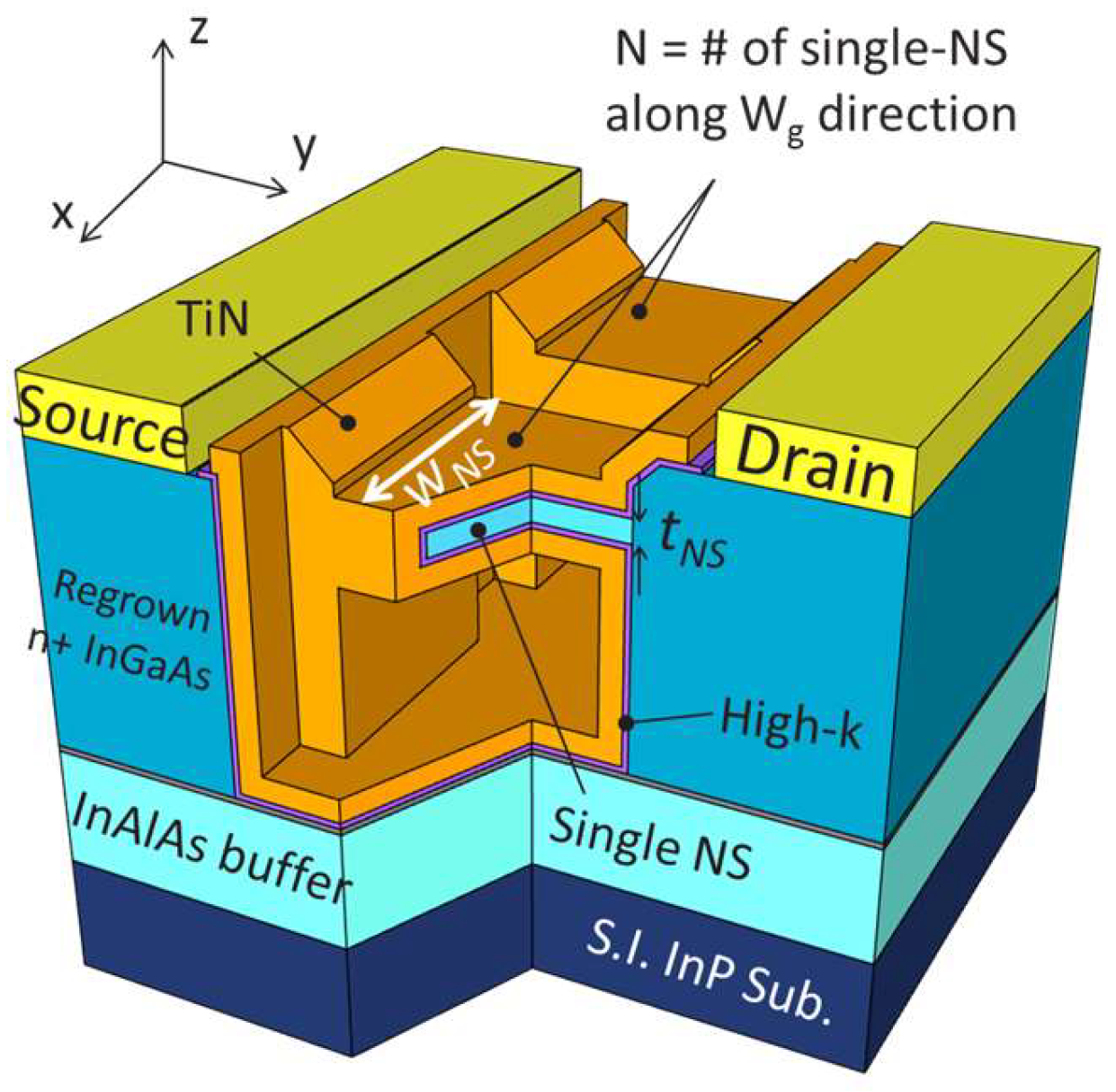
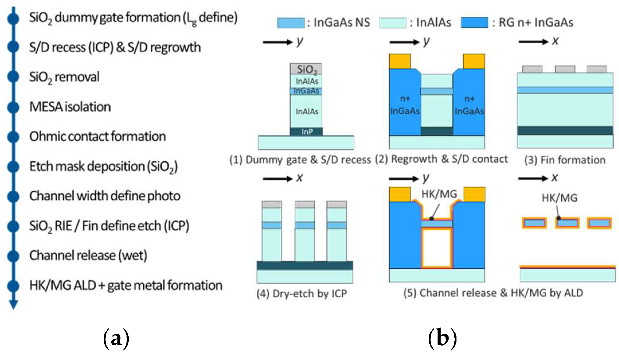
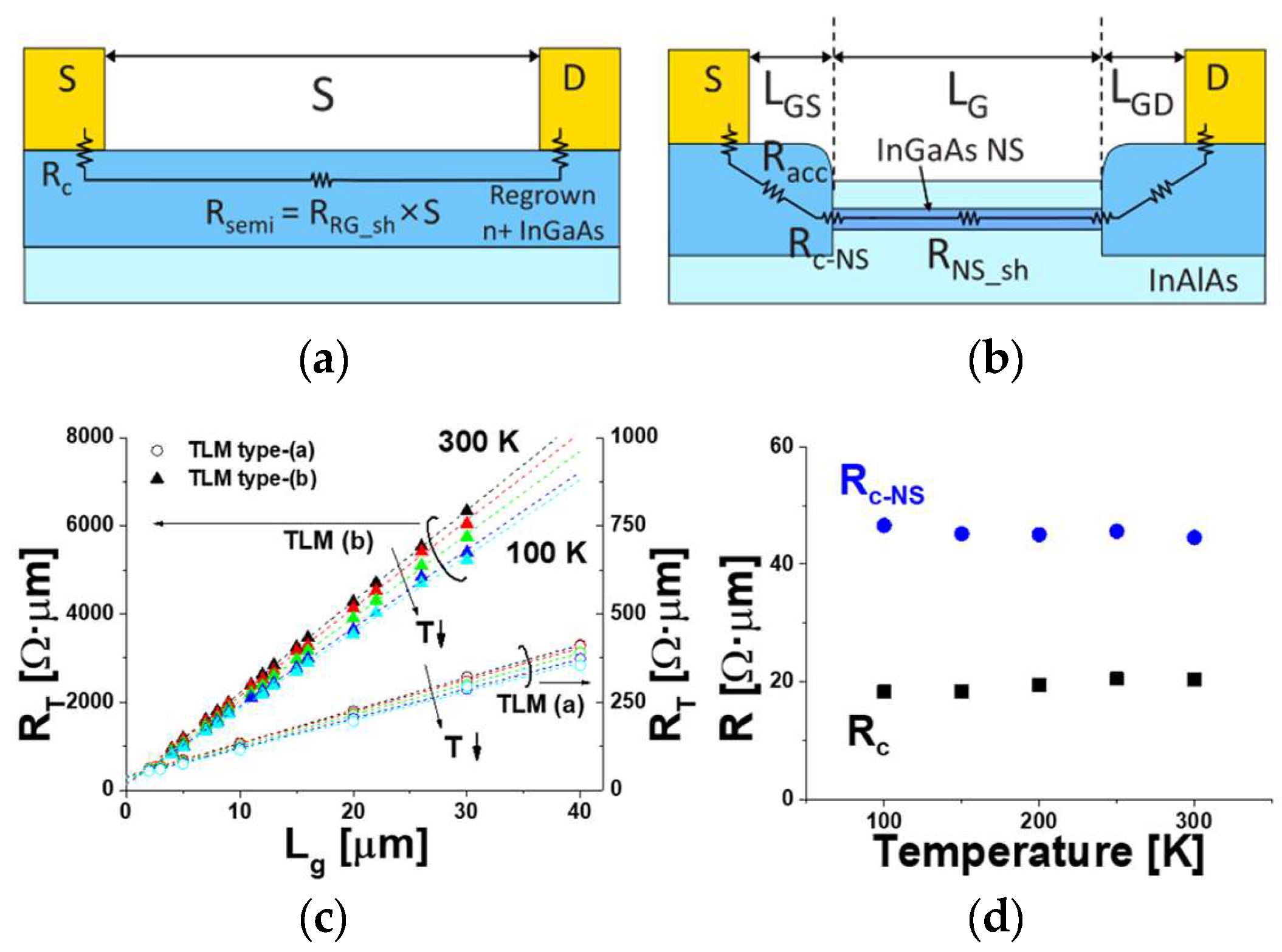
2. Experimental Procedure

Figure 1 illustrates the cross-sectional schematic of a GAA In0.53Ga0.47As NS MOSFET that is in this work. At its heart is a single In0.53Ga0.47As nanosheet layer that is electrically connected to both n+ In0.53Ga0.47As S/D contact layers. Geometrical definitions of WNS (width of a unit NS) and tNS (thickness of a unit NS) are also provided in Figure 1. For a choice of the sacrificial layer, we selected an In0.52Al0.48As layer to avoid an intermixing problem during the growth of the In0.53Ga0.47As/InP QW layer that was achieved via MOCVD technique that prevented the InP sacrificial layers from being removed isotropically. Both sidewalls of the In0.53Ga0.47As NS channel layer along the 011 direction were electrically in contact with the n+ In0.53Ga0.47As layers that were regrown selectively using a MOCVD technique with a Te concentration of 5 × 1019 cm−3, at a relatively high growth temperature of 600 °C. This growth condition helped to not only enable selective epitaxy of the regrown n+ In0.53Ga0.47As layers, except for an SiO2 dummy active area, but also effectively remove the native oxides on the exposed sidewall surfaces of the In0.53Ga0.47As/In0.52Al0.48As QW along the 011 direction and the exposed surface of an InP etch-stopper along the 100 direction, respectively.
Next, this section explains in detail the fabrication procedure to demonstrate the GAA In0.53Ga0.47As NS MOSFETs that are proposed in this work. Figure 2 highlights a process flow and key unit process steps. From bottom to top, the epitaxial layer structure that was used for the device fabrication consisted of a 50-nm-thick bottom In0.52Al0.48As sacrificial layer, a 10 nm-thick-In0.53Ga0.47As nanosheet channel layer and a 50-nm-thick upper In0.52Al0.48As sacrificial layer. First, line and space patterns were defined using a positive photo-resist (PR) on a plasma-enhanced-chemical-vapor-deposition (PECVD)-grown SiO2 layer, where the opened SiO2 area was etched by CF4/Ar-based plasma and the remaining PR was stripped. Subsequently, the exposed In0.52Al0.48As/In0.53Ga0.47As epilayers were etched vertically by BCl3/SiCl4-based ICP at 200 °C, and heavily-doped In0.53Ga0.47As epilayers were regrown in the MOCVD chamber at 600 °C. After the MESA isolation and ohmic contact formation process, both upper and lower In0.52Al0.48As sacrificial layers were exposed through the same BCl3/SiCl4-based ICP process. Then, the exposed upper and bottom In0.52Al0.48As sacrificial layers were etched with a mixture of HCl:DI, releasing the In0.53Ga0.47As nanosheet. Finally, the device fabrication was completed with the deposition of a bi-layer dielectric stack of Al2O3/HfOx that was 1/4 nm and a 30-nm thick TiN metal gate by ALD, in a cross-coupled manner. Figure 3 shows the cross-sectional and top-down TEM/SEM images for the fabricated GAA In0.53Ga0.47As NS MOSFET along the gate-width (Wg, x-direction) and S/D directions (y-direction).

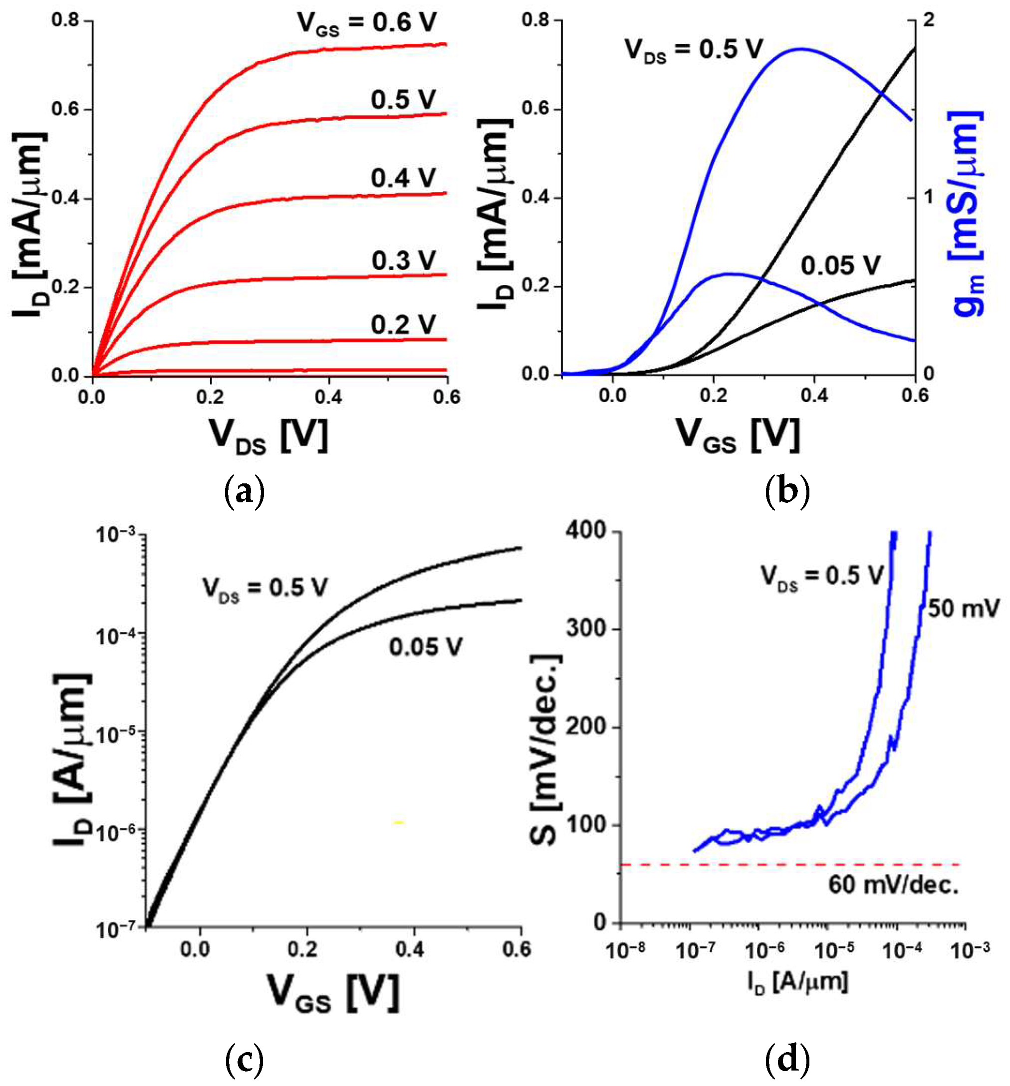
3. Results and Discussion

Figure 4 exhibits two types of transmission line method (TLM) test structures: one TLM structure was used to evaluate the sheet resistance of the regrown n+ InGaAs layer (RRG_sh) and the contact resistance (Rc) between the non-alloyed ohmic of a Ti/Mo/Ti/Pt/Au metal stack and the regrown n+ In0.53Ga0.47As layer (Figure 4a), and the other TLM structure was used to evaluate the actual source resistance (Rs) for the fabricated GAA In0.53Ga0.47As NS MOSFET (Figure 4b) with a dimension of LGS = 0.5 μm. The TLM structure shown in Figure 4b was effective in characterizing the regrown contact resistance of Rc-NS. Here, Rc-NS stands for a contact resistance between the regrown n+ In0.53Ga0.47As layer and the In0.53Ga0.47As NS along the 011 direction. Figure 4c plots the measured total resistance of both structures for various temperatures. Here, half of the y-intercept in the TLM structure shown in Figure 4b corresponds to the sum of Rc, Racc and Rc-NS. Note that both Rc and RRG_sh were obtained from the TLM structure shown in Figure 4a, whereas Racc was calculated by using a formula of Racc = RRG_sh × LGS. Figure 4d shows the extracted Racc and Rc-NS as a function of temperature, where both Rc and Rc-NS are independent of temperature. As in [16], Rc-NS is given by as follows:
R c N S 1 2 h q 2 1 n 2 D E G  
Note that Rc-NS is a function of only two-dimensional electron gas density (n2-DEG) in the In0.53Ga0.47As NS and a measured value of Rc-NS = 45 Ω⋅μm is the same as the theoretical calculation of 45 Ω⋅μm with n2-DEG of 3.3 × 1012 cm−2.
Figure 5a shows the DC output characteristics of the fabricated Lg = 50 nm GAA In0.53Ga0.47As NS MOSFET with WNS = 200 nm and tNS = 10 nm. Here, the device characteristics were normalized by the footprint of the NS channel, as is suggested in [8]. The device exhibited a small value of RON = 206 Ω⋅μm, and excellent pinch-off and saturation behavior. Figure 5b–d exhibit transfer/transconductance, subthreshold characteristics and subthreshold-swing (S) as a function of ID for the same device, respectively. The device delivers a maximum transconductance (gm_max) of 1.86 mS/μm and a subthreshold-swing (S) of 78 mV/dec at VDS = 0.5 V. The ON-current (ION) was extracted using a criteria of VDD = 0.5 V and IOFF = 100 nA/μm. This is a unique figure-of-merit (FOM) that integrates short-channel effects, the parasitic resistance portion and carrier transport of the channel material. The GAA In0.53GA0.47As NS MOSFET that is in this work delivers ION as high as 0.4 mA/μm at VDD = 0.5 V.
Figure 6a–c, respectively, benchmark gm_max vs. minimum dimension, ION vs. Lg and gm_max vs. S, in comparison to those of previously reported non-planar InxGa1-xAs Fin or NW MOSFETs [5,14,15,17,18,19,20,21,22,23,24,25]. Q was defined as gm_max/S, which integrates carrier transport property and electrostatic integrity, as proposed is in [26]. The GAA In0.53Ga0.47As NS MOSFET that is in this work exhibits excellent balance of gm_max, S and ION. In particular, the device in this work displays the highest Q value in any non-planar InxGa1-xAs MOSFET technology.

4. Conclusions

In this paper, we reported a fabrication and electrical characterization of a GAA In0.53Ga0.47As NS MOSFET. The fabricated device with Lg = 50 nm, WNS = 200 nm and tNS = 10 nm exhibited a fairly steep subthreshold-swing of 78 mV/decade, gm_max of 1.86 mS/μm, ION = 0.4 mA/μm and Q = 23 at VDS = 0.5 V. To the best of our knowledge, these metrics represent the best balance of S, gm_max and ION among any InxGa1-xAs-based non-planar MOSFET technology that would be directly applicable to future MBCFETs.

Author Contributions

Conceptualization, I.-G.L., H.-B.J., C.-S.S. and D.-H.K. (Dae-Hyun Kim); Formal analysis, S.-T.L.; Funding acquisition, C.-S.S., K.-S.S. and D.-H.K. (Dae-Hyun Kim); Investigation, J.-M.B., S.-M.C., H.-J.K., W.-S.P., J.-H.Y. and S.-K.K.; Methodology, C.-S.S.; Project administration, I.-G.L.; Resources, S.-T.L., S.-K.K., J.-G.K., J.Y., T.K. and D.-H.K. (Dae-Hyun Kim); Supervision, D.-H.K. (Dae-Hong Ko), T.-W.K., J.-H.L. (Jung-Hee Lee), C.-S.S., J.-H.L. (Jae-Hak Lee) and K.-S.S.; Writing – original draft, I.-G.L., H.-B.J. and D.-H.K. (Dae-Hyun Kim); Writing—review & editing, I.-G.L. and H.-B.J. All authors have read and agreed to the published version of the manuscript.

Funding

This work was supported by the Nano-Material Technology Development Program through the National Research Foundation of Korea (NRF) funded by the Ministry of Science and ICT (NRF-2017M3A7B4049517).

Institutional Review Board Statement

Not applicable.

Informed Consent Statement

Not applicable.

Data Availability Statement

The data presented in this study are available on request from the corresponding author.

Conflicts of Interest

The authors declare no conflict of interest.

References

  1. Auth, C.; Aliyarukunju, A.; Asoro, M.; Bergstrom, D.; Bhagwat, V.; Birdsall, J.; Bisnik, N.; Buehler, M.; Chikarmane, V.; Ding, G.; et al. A 10nm High Performance and Low-Power CMOS Technology Featuring 3rd Generation FinFET Transistors, Self-Aligned Quad Patterning, Contact over Active Gate and Cobalt Local Interconnects. In Proceedings of the 2017 IEEE International Electron Devices Meeting (IEDM), San Francisco, CA, USA, 2–6 December 2017; pp. 29.1.1–29.1.4. [Google Scholar]
  2. Hashemi, P.; Ando, T.; Balakrishnan, K.; Cartier, E.; Lofaro, M.; Ott, J.A.; Bruley, J.; Lee, K.-L.; Koswatta, S.; Dawes, S.; et al. Replacement High-K/Metal-Gate High-Ge-Content Strained SiGe FinFETs with High Hole Mobility and Excellent SS and Reliability at Aggressive EOT ∼7Å and Scaled Dimensions down to Sub-4nm Fin Widths. In Proceedings of the 2016 IEEE Symposium on VLSI Technology, Honolulu, HI, USA, 14–16 June 2016; pp. 1–2. [Google Scholar]
  3. Vardi, A.; Kong, L.; Lu, W.; Cai, X.; Zhao, X.; Grajal, J.; del Alamo, J.A. Self-Aligned InGaAs FinFETs with 5-nm Fin-Width and 5-nm Gate-Contact Separation. In Proceedings of the 2017 IEEE International Electron Devices Meeting (IEDM), San Francisco, CA, USA, 2–6 December 2017; pp. 17.6.1–17.6.4. [Google Scholar]
  4. Hahn, H.; Deshpande, V.; Caruso, E.; Sant, S.; O’Connor, E.; Baumgartner, Y.; Sousa, M.; Caimi, D.; Olziersky, A.; Palestri, P.; et al. A Scaled Replacement Metal Gate InGaAs-on-Insulator n-FinFET on Si with Record Performance. In Proceedings of the 2017 IEEE International Electron Devices Meeting (IEDM), San Francisco, CA, USA, 2–6 December 2017; pp. 17.5.1–17.5.4. [Google Scholar]
  5. Lu, W.; Roh, I.P.; Geum, D.-M.; Kim, S.-H.; Song, J.D.; Kong, L.; del Alamo, J.A. 10-nm Fin-Width InGaSb p-Channel Self-Aligned FinFETs Using Antimonide-Compatible Digital Etch. In Proceedings of the 2017 IEEE International Electron Devices Meeting (IEDM), San Francisco, CA, USA, 2–6 December 2017; pp. 17.7.1–17.7.4. [Google Scholar]
  6. Lee, S.; Cheng, C.-W.; Sun, X.; D’Emic, C.; Miyazoe, H.; Frank, M.M.; Lofaro, M.; Bruley, J.; Hashemi, P.; Ott, J.A.; et al. High Performance InGaAs Gate-All-Around Nanosheet FET on Si Using Template Assisted Selective Epitaxy. In Proceedings of the 2018 IEEE International Electron Devices Meeting (IEDM), San Francisco, CA, USA, 1–5 December 2018; pp. 39.5.1–39.5.4. [Google Scholar]
  7. Kanazawa, T.; Ohsawa, K.; Amemiya, T.; Kise, N.; Aonuma, R.; Miyamoto, Y. Fabrication of InGaAs Nanosheet Transistors with Regrown Source. In Proceedings of the Compound Semiconductor Week (CSW), Cambridge, MA, USA, 29 May–1 June 2018; p. We3C3.2. [Google Scholar]
  8. Loubet, N.; Hook, T.; Montanini, P.; Yeung, C.-W.; Kanakasabapathy, S.; Guillom, M.; Yamashita, T.; Zhang, J.; Miao, X.; Wang, J.; et al. Stacked Nanosheet Gate-All-Around Transistor to Enable Scaling beyond FinFET. In Proceedings of the 2017 Symposium on VLSI Technology, Kyoto, Japan, 5–8 June 2017; pp. T230–T231. [Google Scholar]
  9. Tsai, C.-E.; Liu, Y.-C.; Tu, C.-T.; Huang, B.-W.; Jan, S.-R.; Chen, Y.-R.; Chen, J.-Y.; Chueh, S.-J.; Cheng, C.-Y.; Tsen, C.-J.; et al. Highly Stacked 8 Ge0.9Sn0.1 Nanosheet PFETs with Ultrathin Bodies (~3nm) and Thick Bodies (~30nm) Featuring the Respective Record ION/IOFF of 1.4 × 10⁷ and Record ION of 92 μA/ at VOV=VDS=-0.5V by CVD Epitaxy and Dry Etching. In Proceedings of the 2021 IEEE International Electron Devices Meeting (IEDM), San Francisco, CA, USA, 11–16 December 2021; pp. 26.4.1–26.4.4. [Google Scholar]
  10. Agrawal, A.; Chouksey, S.; Rachmady, W.; Vishwanath, S.; Ghose, S.; Mehta, M.; Torres, J.; Oni, A.A.; Weng, X.; Li, H.; et al. Gate-All-Around Strained Si0.4Ge0.6 Nanosheet PMOS on Strain Relaxed Buffer for High Performance Low Power Logic Application. In Proceedings of the 2020 IEEE International Electron Devices Meeting (IEDM), San Francisco, CA, USA, 12–18 December 2020; pp. 2.2.1–2.2.4. [Google Scholar]
  11. Del Alamo, J.A. Nanometre-Scale Electronics with III–V Compound Semiconductors. Nature 2011, 479, 317. [Google Scholar] [CrossRef] [PubMed]
  12. Lin, J.; Zhao, X.; Yu, T.; Antoniadis, D.A.; del Alamo, J.A. A New Self-Aligned Quantum-Well MOSFET Architecture Fabricated by a Scalable Tight-Pitch Process. In Proceedings of the 2013 IEEE International Electron Devices Meeting, Washington, DC, USA, 9–11 December 2013; pp. 16.2.1–16.2.4. [Google Scholar]
  13. Xuan, Y.; Wu, Y.Q.; Ye, P.D. High-Performance Inversion-Type Enhancement-Mode InGaAs MOSFET With Maximum Drain Current Exceeding 1 A/mm. IEEE Electron. Device Lett. 2008, 29, 294–296. [Google Scholar] [CrossRef]
  14. Tomioka, K.; Yoshimura, M.; Fukui, T. A III–V Nanowire Channel on Silicon for High-Performance Vertical Transistors. Nature 2012, 488, 189–192. [Google Scholar] [CrossRef] [PubMed]
  15. Ramesh, S.; Ivanov, T.; Putcha, V.; Alian, A.; Sibaja-Hernandez, A.; Rooyackers, R.; Camerotto, E.; Milenin, A.; Pinna, N.; Kazzi, S.E.; et al. Record Performance Top-down In0.53Ga0.47As Vertical Nanowire FETs and Vertical Nanosheets. In Proceedings of the 2017 IEEE International Electron Devices Meeting (IEDM), San Francisco, CA, USA, 2–6 December 2017; pp. 17.1.1–17.1.4. [Google Scholar]
  16. Solomon, P.M.; Palevski, A.; Kuech, T.F.; Tischler, M.A. Low Resistance Ohmic Contacts to Two-Dimensional Electron-Gas Structures by Selective MOVPE. In Proceedings of the International Technical Digest on Electron Devices Meeting, Washington, DC, USA, 3–6 December 1989; pp. 405–408. [Google Scholar]
  17. Lu, W.; Lee, Y.; Murdzek, J.; Gertsch, J.; Vardi, A.; Kong, L.; George, S.M.; del Alamo, J.A. First Transistor Demonstration of Thermal Atomic Layer Etching: InGaAs FinFETs with Sub-5 nm Fin-Width Featuring in Situ ALE-ALD. In Proceedings of the 2018 IEEE International Electron Devices Meeting (IEDM), San Francisco, CA, USA, 1–5 December 2018; pp. 39.1.1–39.1.4. [Google Scholar]
  18. Huang, M.L.; Chang, S.W.; Chen, M.K.; Oniki, Y.; Chen, H.C.; Lin, C.H.; Lee, W.C.; Lin, C.H.; Khaderbad, M.A.; Lee, K.Y.; et al. High Performance In0.53Ga0.47As FinFETs Fabricated on 300 mm Si Substrate. In Proceedings of the 2016 IEEE Symposium on VLSI Technology, Honolulu, HI, USA, 14–16 June 2016; pp. 1–2. [Google Scholar]
  19. Sun, X.; D’Emic, C.; Cheng, C.-W.; Majumdar, A.; Sun, Y.; Cartier, E.; Bruce, R.L.; Frank, M.; Miyazoe, H.; Shiu, K.-T.; et al. High Performance and Low Leakage Current InGaAs-on-Silicon FinFETs with 20 nm Gate Length. In Proceedings of the 2017 Symposium on VLSI Technology, Kyoto, Japan, 5–8 June 2017; pp. T40–T41. [Google Scholar]
  20. Kilpi, O.; Svensson, J.; Wernersson, L. Sub-100-nm Gate-Length Scaling of Vertical InAs/InGaAs Nanowire MOSFETs on Si. In Proceedings of the 2017 IEEE International Electron Devices Meeting (IEDM), San Francisco, CA, USA, 2–6 December 2017; pp. 17.3.1–17.3.4. [Google Scholar]
  21. Ramesh, S.; Ivanov, T.; Camerotto, E.; Sun, N.; Franco, J.; Sibaja-Hernandez, A.; Rooyackers, R.; Alian, A.; Loo, J.; Veloso, A.; et al. Top-down InGaAs Nanowire and Fin Vertical FETs with Record Performance. In Proceedings of the 2016 IEEE Symposium on VLSI Technology, Honolulu, HI, USA, 14–16 June 2016; pp. 1–2. [Google Scholar]
  22. Tomioka, K.; Motohisa, J.; Fukui, T. III-V Nanowire Channel on Si: From High-Performance Vertical FET to Steep-Slope Devices. In Proceedings of the 2015 International Symposium on VLSI Technology, Systems and Applications, Hsinchu, Taiwan, 27–29 April 2015; pp. 1–2. [Google Scholar]
  23. Persson, K.-M.; Berg, M.; Borg, M.B.; Wu, J.; Johansson, S.; Svensson, J.; Jansson, K.; Lind, E.; Wernersson, L.-E. Extrinsic and Intrinsic Performance of Vertical InAs Nanowire MOSFETs on Si Substrates. IEEE Trans. Electron. Devices 2013, 60, 2761–2767. [Google Scholar] [CrossRef]
  24. Thelander, C.; Fröberg, L.E.; Rehnstedt, C.; Samuelson, L.; Wernersson, L.-E. Vertical Enhancement-Mode InAs Nanowire Field-Effect Transistor With 50-nm Wrap Gate. IEEE Electron. Device Lett. 2008, 29, 206–208. [Google Scholar] [CrossRef]
  25. Berg, M.; Persson, K.; Kilpi, O.; Svensson, J.; Lind, E.; Wernersson, L. Self-Aligned, Gate-Last Process for Vertical InAs Nanowire MOSFETs on Si. In Proceedings of the 2015 IEEE International Electron Devices Meeting (IEDM), Washington, DC, USA, 7–9 December 2015; pp. 31.2.1–31.2.4. [Google Scholar]
  26. Doornbos, G.; Passlack, M. Benchmarking of III–V n-MOSFET Maturity and Feasibility for Future CMOS. IEEE Electron. Device Lett. 2010, 31, 1110–1112. [Google Scholar] [CrossRef]
Figure 1. The 3D cross-sectional schematic of a GAA In0.53Ga0.47As NS MOSFET that is in this work, together with geometrical definitions such as WNS and tNS.
Electronics 11 02744 g001
Figure 2. (a) Process flow and (b) key unit process steps of the GAA In0.53Ga0.47As NS MOSFETs that are in this work.
Electronics 11 02744 g002
Figure 3. Cross-sectional and top-down TEM/SEM images of the fabricated GAA In0.53Ga0.47As NS MOSFETs along the Wg (x-direction, (a)) and S/D (y-direction, (be)) directions, and EDS mapping data (f).
Electronics 11 02744 g003
Figure 4. Two TLM structures for (a) regrown n+ In0.53Ga0.47As and (b) single-NS, (c) the measured total resistance for both TLM structures and (d) temperature dependence of the extracted Rc and Rc-NS.
Electronics 11 02744 g004
Figure 5. The measured DC behavior of the Lg = 50 nm GAA In0.53Ga0.47As NS MOSFET: (a) output characteristics, (b) transfer/transconductance characteristics, (c) subthreshold characteristics and (d) subthreshold-swing (S) against ID.
Electronics 11 02744 g005
Figure 6. Benchmark of (a) gm_max vs. minimum dimensions (WFin or tNS), (b) ION vs. Lg and (c) gm_max vs. S against those of other groups’ non-planar InxGa1-xAs MOSFETs.
Electronics 11 02744 g006
Publisher’s Note: MDPI stays neutral with regard to jurisdictional claims in published maps and institutional affiliations.

