Article

Fault Diagnosis and Tolerant Control for Three-Level T-Type Inverters

Department of Electrical Engineering, National Chin-Yi University of Technology, Taichung 41170, Taiwan
*
Author to whom correspondence should be addressed.
Electronics 2022, 11(16), 2496; https://doi.org/10.3390/electronics11162496
Submission received: 31 May 2022 / Revised: 28 July 2022 / Accepted: 28 July 2022 / Published: 10 August 2022

Abstract

:
This paper proposes a fault diagnosis system for inverters based on a cerebellar model articulation controller (CMAC). First, a three-level T-type inverter was implemented and used to create a three-level T-type inverter test environment for measuring the output voltage waveforms of faulty power transistors on the main inverter circuit under different output frequencies. The measured waveforms were processed using a fast Fourier transform (FFT) algorithm to create frequency spectrum diagrams and extract the characteristic spectra of corresponding faulty switches. Then, the associations of the spectra were determined and applied as training data for the CMAC to detect the positions of the faulty power transistors. The test results demonstrated that the proposed induction motor fault diagnosis system is capable of fast algorithm, requires less data to train, and has excellent accuracy of identification, with an error margin of ±5%. The detection results were then processed using a fault-tolerant controller (FTC) to enhance the reliability of the proposed system. Finally, some simulations and experimental results were conducted and analyzed to validate the feasibility of the proposed FTC system.

1. Introduction

Compared with two-level inverters, multi-level inverters [1,2,3,4,5] demonstrate reduced voltage stress on the switches and change in output voltage (dv/dt). They are suitable for high-power applications, and their cascaded arrangement of power transistors facilitate the formation of step-shaped wavelets in the output line-to-neutral point voltage waveform, creating trapezoidal voltage waveforms (similar to sine waveforms) that reduce harmonic content. Multi-level inverters can be categorized into diode-clamped, T-type, cascaded h-bridge (CHB), and flying capacitor inverters. Among these categories, the three-level, diode-clamped inverter is a widely applied inverter that is simple and easy to control [6]. This type of inverter is equipped with a capacitor that evenly divides the voltage from the direct current (DC) side into three voltage levels (+Vdc/2, 0, and −Vdc/2). Therefore, the output voltage comprises three states and requires diodes and switches to clamp the output voltage of the inverter to the neutral-point voltage of the DC side. The three-level T-type inverter proposed by Schweizer and Kolar [7], which is an inverter that does not require diode clamping, was examined in this paper. This inverter adopts common emitter-cascaded power transistors to achieve neutral-point voltage clamping rather than the use of additional diodes by diode-clamped inverters. The three-level T-type inverter effectively enhances the reliability and reduces the cost of the system. However, factors such as extended overcurrent (high temperature) operations, component aging, and drive circuit malfunction may damage the switches and hinder normal operations. To resolve these issues, multi-level inverter designs must take into account fault detection mechanisms and fault-tolerant control (FTC) capabilities to ensure that the inverter can maintain normal operations when a fault occurs [8,9,10].
Number or waveforms were directly used to represent the fault diagnosis information produced by early measuring instruments for the motor drive system. Fault points can be detected quickly and easily using these results. However, experienced personnel must be present to interpret the diagnostic information, detect the fault type, and engage in the maintenance or replacement of relevant components. This traditional fault diagnosis method has often led to detection error and waste of time and manpower for unnecessary maintenance and replacement [11,12,13]. Therefore, developing new techniques to diagnose system faults has been a longstanding focus of research. A number of scholars in Taiwan and other countries have centered their efforts on developing new diagnostic techniques [14,15,16,17]. Extant fault detection and diagnosis methods can be characterized into three major types, specifically, model-based techniques, expert system, and artificial intelligence (AI) algorithms. Model-based techniques are effective diagnostic methods. However, assumptions and limitations are unavoidable in model-based techniques due to the difficulty of building inverter models (including snubber capacitance and balance resistors) and the parasitic nature of inverters. Expert systems are often used in large systems. They effectively adjust systems but require experts to construct the entire system, which can be extremely costly. By comparison, AI algorithms require neither models nor expert knowledge [18,19,20,21]. Rather, they rely on the initial training data of normal and abnormal conditions, making them extremely versatile. A variety of AI algorithms is available, including the fuzzy method [22,23] and the neuro-fuzzy method [24]. These methods can be used to establish a fault diagnosis system solely based on the associations between input and output. However, the accuracy of algorithms increases over time. They are also limited to diagnosing single datasets at a given time and rely on expert experience. To overcome these limitations, this paper proposes a CMAC-based fault diagnosis method that adopts fast-learning and highly responsive AI algorithms.
A three-level T-type inverter was used to test the performance of the proposed system in detecting the positions of faulty power transistors. Subsequently, an FTC was used to maintain the operation reliability of the inverter. The CMAC-based fault diagnosis system for inverters architecture is illustrated in Figure 1.

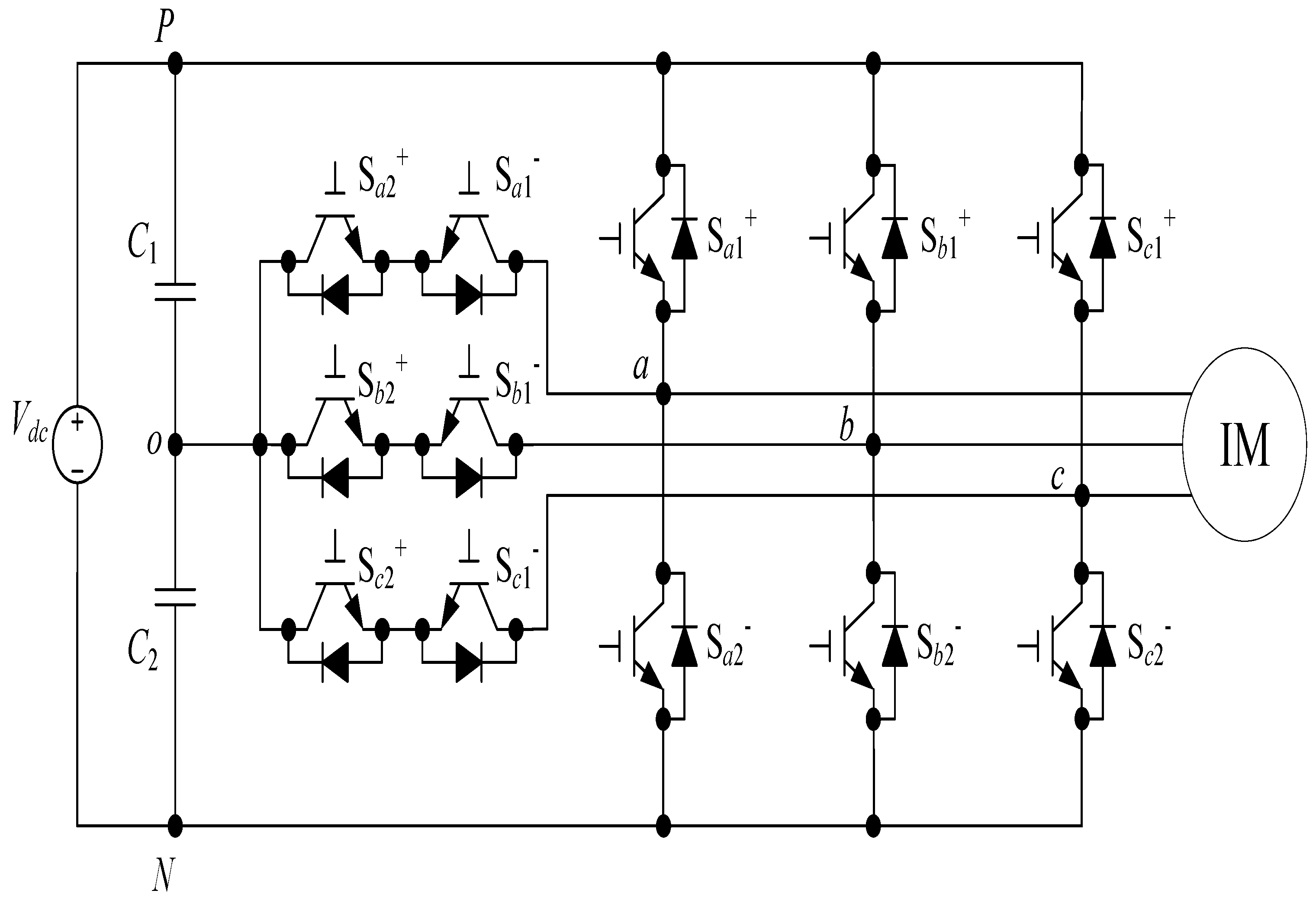
2. Fault Characteristics of Three-Level Inverters

The three-level T-type inverter circuit illustrated in Figure 2 was used to analyze the fault diagnosis system. The time command pulse width modulation (PWM) scheme of switches is generated using the comparison between the three-phase balanced sinusoidal waves (vsin_a, vsin_b, and vsin_c) and triangular waves (vtri_1 and vtri_2) as shown in Figure 3. In addition, the SX1+ and SX1, and SX2+ and SX2 must be controlled into a complementary state. Take a-phase as an example: when vsin_a > vtri_1, let the power transistors Sa1+ and Sa2+ be turned on and Sa1 and Sa2 be turned off. If vtri_1 > vsin_a > vtri_2, let the power transistors Sa2+ and Sa1 be turned on and Sa1+ and Sa2 be turned off. However, if vsin_a < vtri_2, then let the power transistors Sa1 and Sa2 be turned on and Sa1+ and Sa2+ be turned off. The power transistors of b-phase and c-phase can be controlled with the same control strategy. Generally, inverter faults can largely be categorized into three types, namely, short-circuit fault, open-circuit fault, and trigger signal mistransmission. Short-circuit faults occur when an excessive electrical voltage travels through a switch without resistance. Open-circuit faults occur when power transistors fail to transmit trigger signals to the appropriate channels. Trigger signal mistransmission occurred when switches received erroneous trigger commands.
A practical three-level T-type inverter was implemented and used to create a test environment. A switch fault at a random point in time was tested. Measured outcomes indicated that the waveforms produced by the inverter achieved three-phase balance during normal operation. When the inverter operated at a working frequency of 60 Hz without faulty power transistors, the inverter produced output waveforms and frequency spectra similar to those illustrated in Figure 4 and Figure 5. Figure 4 shows that the size and shape of the various phase voltage waveforms were similar with a mutual phase difference of 120°. These are typical three-phase balance characteristics. When a fault occurs in any of the switches in the inverter, the characteristics in Figure 4 would change. For example, when a fault occurred in switch Sa1+, the waveform of the a-phase output voltage (vao) distorted (Figure 6). Figure 7 illustrates the waveform of the b-phase voltage (vbo) when a fault occurred in switch Sb2. The figure clearly shows a significant difference between the waveform of the voltage (vbo) during normal and faulty conditions. Figure 8 illustrates the waveform of the c-phase voltage (vco) when a fault occurred in switch Sc1+. The figure clearly shows waveform distortion in the output phase voltage of the c arm (vco). The waveform of the a-phase output voltage (vao) of the inverter with a fault in switch Sa1+ shown in Figure 6 is same as the waveform of the c-phase output voltage (vco) of the inverter with a fault in switch Sc1+ shown in Figure 8, but the phase difference is 120°.
The preceding analysis confirmed the presence of abnormalities in the voltage frequency spectra of the inverter during the occurrence of a fault. Figure 9 illustrates the frequency spectra of the various phase voltages when a fault occurs in switch Sc1+ at a working frequency of 60 Hz. A comparison between the frequency spectra of Figure 9 and those of the inverter during normal operation (Figure 5) revealed increased variance at (mf − 1)th and (mf + 1)th order of the frequency spectra for phase voltage vco. Therefore, the spectral values at a working frequency of 60 Hz were adopted as the characteristic spectra for faults. Subsequently, m f was defined as the frequency modulation index. The index can be expressed as follows:
m f = Δ f c a r r i e r f r e f e r e n c e = f t r i f s i n
where, ftri represents the frequency of the triangular carrier wave (or the switching frequency of the inverter), and fsin represents the frequency of the sine wave (or the working frequency of the inverter). Parameter data concerning power transistor faults can be retrieved from the measured and analysis results. A CMAC was used to create a fault diagnosis system for inverters to detect faults in the main three-level T-type inverter circuit during switching.

3. The Cerebellar Model Articulation Controller
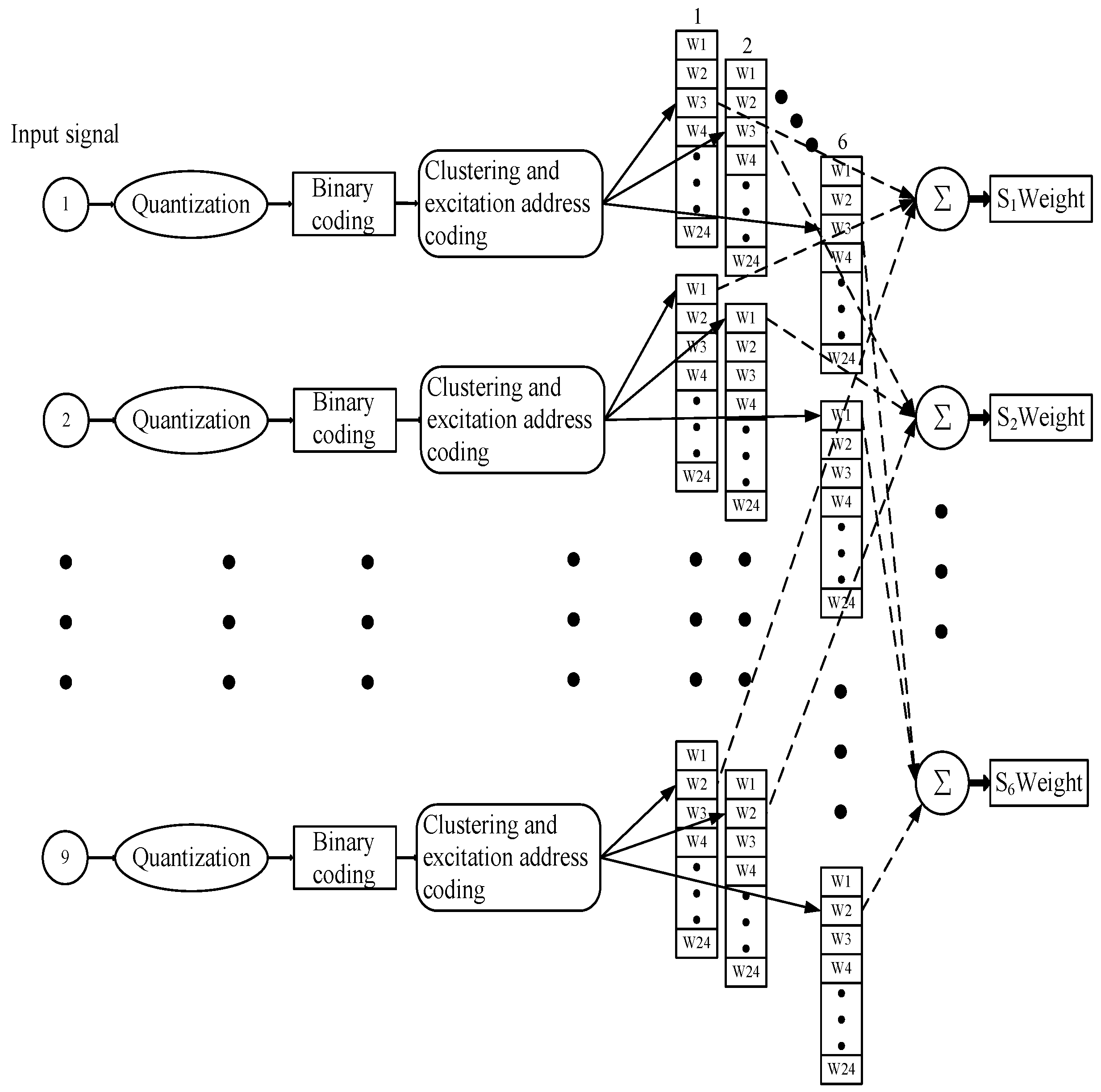
The CMAC was introduced by J. S. Albus in 1970 [25]. The CMAC model mimics the cerebellar neural structure of a human to achieve rapid learning and response characteristics. The CMAC framework is illustrated in Figure 10. The input signals undergo quantization, binary coding, and excitation address coding in the CMAC. The excitation addresses are then summed to generate an output value. The size of the value is analyzed to determine the type of switch fault. Training samples only excite or train their corresponding memory units. For example, the ith (i = 1–6) training sample only excites, trains, or tunes the ith layer. Therefore, overall training time is drastically reduced [26].

3.1. Quantization

A number of equal quantization levels were categorized between the highest and lowest values of the input signals. Quantization levels with higher resolutions are able to produce more detailed quantization codes but demand more free memory. In this paper, the input signals were divided into 255 levels. Levels higher than the maximum value were allocated a quantization value of 255. Levels lower than the minimum value were allocated a value of 0. A corresponding quantization value was allocated to the quantization levels between the maximum and minimum values.

3.2. Excitation Address Coding and CMAC Output Calculation

According to the corresponding quantization levels of the input signals, the values were converted into binary codes. The coded values were then combined and re-coded. Finally, the clusters were provided with a cluster code and an excitation address. For example, the input signals are the voltages at (mf − 1)th and (mf + 1)th orders in the three-phase frequency spectrum. Nine difference values are present between the two voltages. Assuming that the levels after quantization were 209, 200, 10, 5, 3, 10, 5, 6, and 5, they are first converted into binary codes (11010001b, 11001000b, 00001010b, 00000101b, 00000011b, 00001010b, 00000101b, 00000110b, and 00000101b) and then combined and re-coded (110100011100100000001010000001010000001100001010000001010000011000000101b) to obtain a 72-bit code. If the code is clustered every three bits, a total of 24 clusters would be obtained. The excitation addresses for the 24 clusters from the least significant bit (LSB) to the most significant bit (MSB) are n 1 = 101b = 5, n 2 = 000b = 0, n 3 = 000b = 0, n 4 = 011b = 3, n 5 = 000b = 0, n 6 = 010b = 2, n 7 = 001b = 1, n 8 = 000b = 0, n 9 = 010b = 2, n 10 = 001b = 1, n 11 = 100b = 4, n 12 = 001b = 1, n 13 = 000b = 0, n 14 = 010b = 2, n 15 = 001b = 1, n 16 = 000b = 0, n 17 = 010b = 2, n 18 = 001b = 1, n 19 = 000b = 0, n 20 = 100b = 4, n 21 = 100b = 4, n 22 = 011b = 3, n 23 = 100b = 4, and n 24 = 110b = 6. Assuming that the initial weighting of the memory units was 0, then the sum of w 1 5 , w 2 0 , w 3 0 , w 4 3 , w 5 0 , w 6 2 , w 7 1 , w 8 0 , w 9 2 , w 10 1 , w 11 4 , w 12 1 , w 13 0 , w 14 2 , w 15 1 , w 16 0 , w 17 2 , w 18 1 , w 19 0 , w 20 4 , w 21 4 , w 22 3 , w 23 4 , and w 24 6 would be 0. Hence, the CMAC output can be expressed as follows:
y = i = 1 N * w i n i
where y is the actual output value, N * is the number of excitation addresses, w i n i is the weight of the excitation memory, and n i is the address of the excited memory.

3.3. Memory Weight Tuning

The output target for the CMAC was set as 1.0 in this paper. A supervised learning approach can be used for clear output targets. Subsequently, the steepest descent method was adopted to tune the various weights [27], which can be expressed as follows:
w i ( n e w ) n i = w i ( o l d ) n i + β y d y N *   i = 1 ,   2   , ,   N *
where w i ( n e w ) n i is the new weight after tuning the excitation memory, w i ( o l d ) n i is the old weight before tuning the excitation memory, β is the learning gain ( 0 < β 1 ), and y d is the target value.

3.4. Fault Tolerance
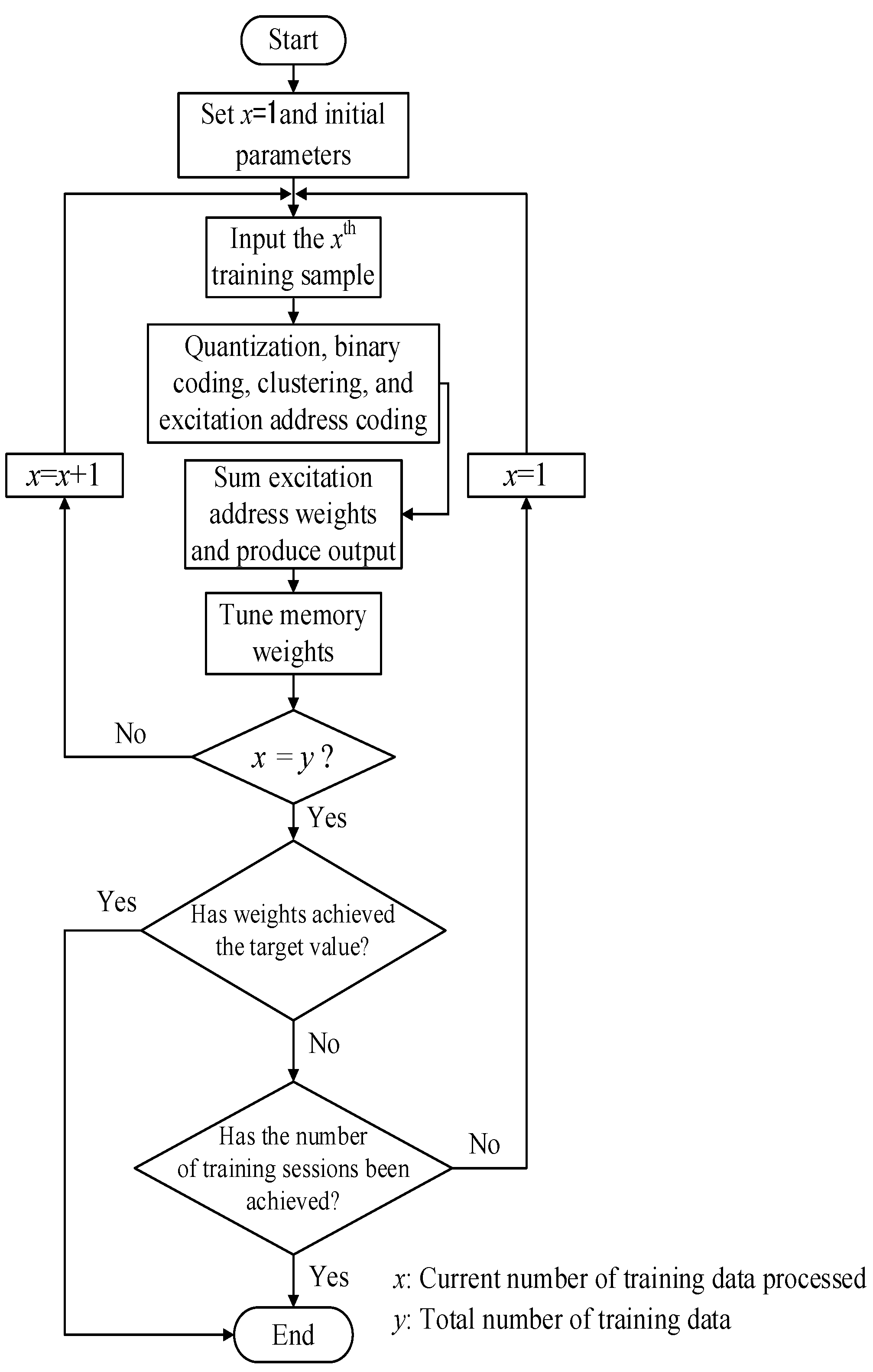
The proposed fault diagnosis method demonstrates excellent interference resistance. Using the 72-bit code characterized in Section 3.2, the original code was changed to 110100011100100000001010000001010000001100001010000001010000011001000101b. After coding the excitation addresses ( n 1 , n 2 , n 3 , n 4 , n 5 , n 6 , n 7 , n 8 , n 9 , n 10 , n 11 , n 12 , n 13 , n 14 , n 15 , n 16 , n 17 , n 18 , n 19 , n 20 , n 21 , n 22 , n 23 , and n 24 ) changed from 5, 0, 0, 3, 0, 2, 1, 0, 2, 1, 4, 1, 0, 2, 1, 0, 2, 1, 0, 4, 4, 3, 4, and 6 to 5, 0, 1, 3, 0, 2, 1, 0, 2, 1, 4, 1, 0, 2, 1, 0, 2, 1, 0, 4, 4, 3, 4, and 6. A fault occurred only n 3 . All other excitation addresses achieved a normal output, suggesting that the method demonstrated excellent fault tolerance. By expanding the number of clusters, the address can be dispersed and stored in more locations, reducing the effects of fault detection in the neighboring bit on output and enhancing accuracy.

3.5. CMAC Training

The training process for the CMAC-based fault diagnosis system for inverters is illustrated in Figure 11. The input training samples first underwent quantization, combined coding, cluster coding, and memory address excitation. The weights of the excitation addresses were then summed to produce an output. Equation (3) was used to tune the memory weights. Once all the samples were trained, the sample weights were analyzed to determine whether the target value was achieved. The training program can be terminated once the target value is achieved. Otherwise, the training program can be terminated once the predetermined number of training sessions has been reached.

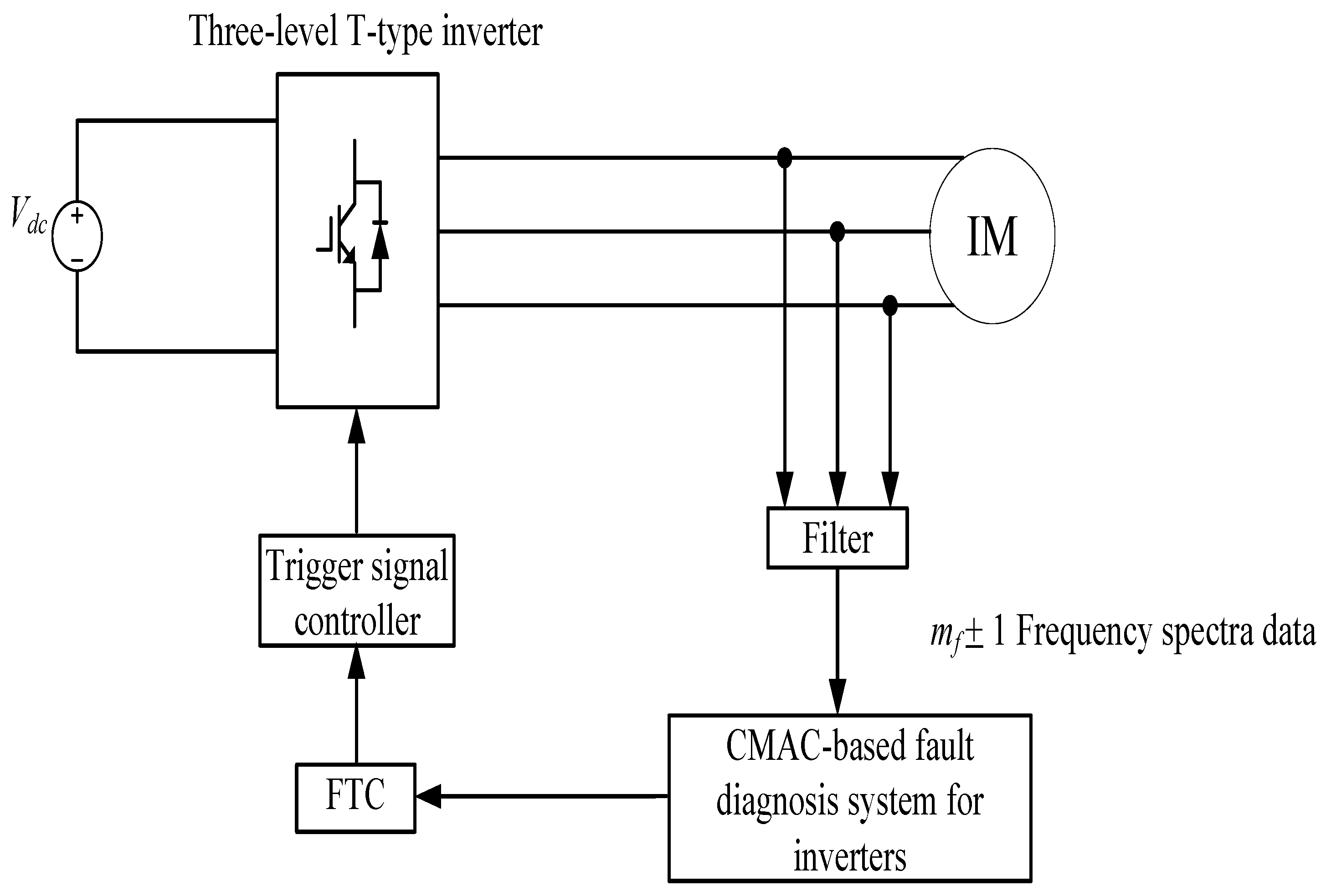
4. CMAC-Based Fault Diagnosis for Inverters

Extended overcurrent (high-temperature) operations or component aging can cause faults in inverters. The three-level T-type inverter structure illustrated in Figure 2 was used to test switch faults. The proposed CMAC-based system was then employed to detect the positions of faulty power transistors.
First, the measured waveforms of the three-phase voltage in the inverter were processed using a fast Fourier transform algorithm to obtain the voltage spectra at (mf − 1)th and (mf + 1)th orders and the difference between them. These values served as the input signals of the CMAC. Switches Sa1+, Sa2, Sb1+, Sb2, Sc1+, and Sc2 served as the different fault types. Moreover, 648 sets of data were collected concerning the faults of the six switches in the inverter at a working frequency between 20 and 90 Hz. The datasets were divided into 432 training data sets and 216 test datasets. The training data sets were processed using the CMAC training model characterized in Section 3.5 to obtain the weights of the different faulty switches. The parameter settings for the CMAC training program are as follows: (1) quantization levels: 255 levels; (2) bits per cluster: 3 bits; (3) cluster quantity: 24 clusters; (4) learning constants ( β ): 1 constant; and (5) training sessions: 25 times.
Fault detection and diagnosis can commence once the CMAC has been trained. The diagnosis procedures are as follows:
  • Step 1. Access the weights of the trained CMAC.
  • Step 2. Access the test data samples.
  • Step 3. Proceed in the quantization, combined coding, clustering, and excitation address coding of the data.
  • Step 4. Sum the weights of the excitation addresses to produce an output.
  • Step 5. Determine the weight of the output (weight value closer to 1 denotes an increased likeliness of fault).
  • Step 6. Generate fault diagnostic results.
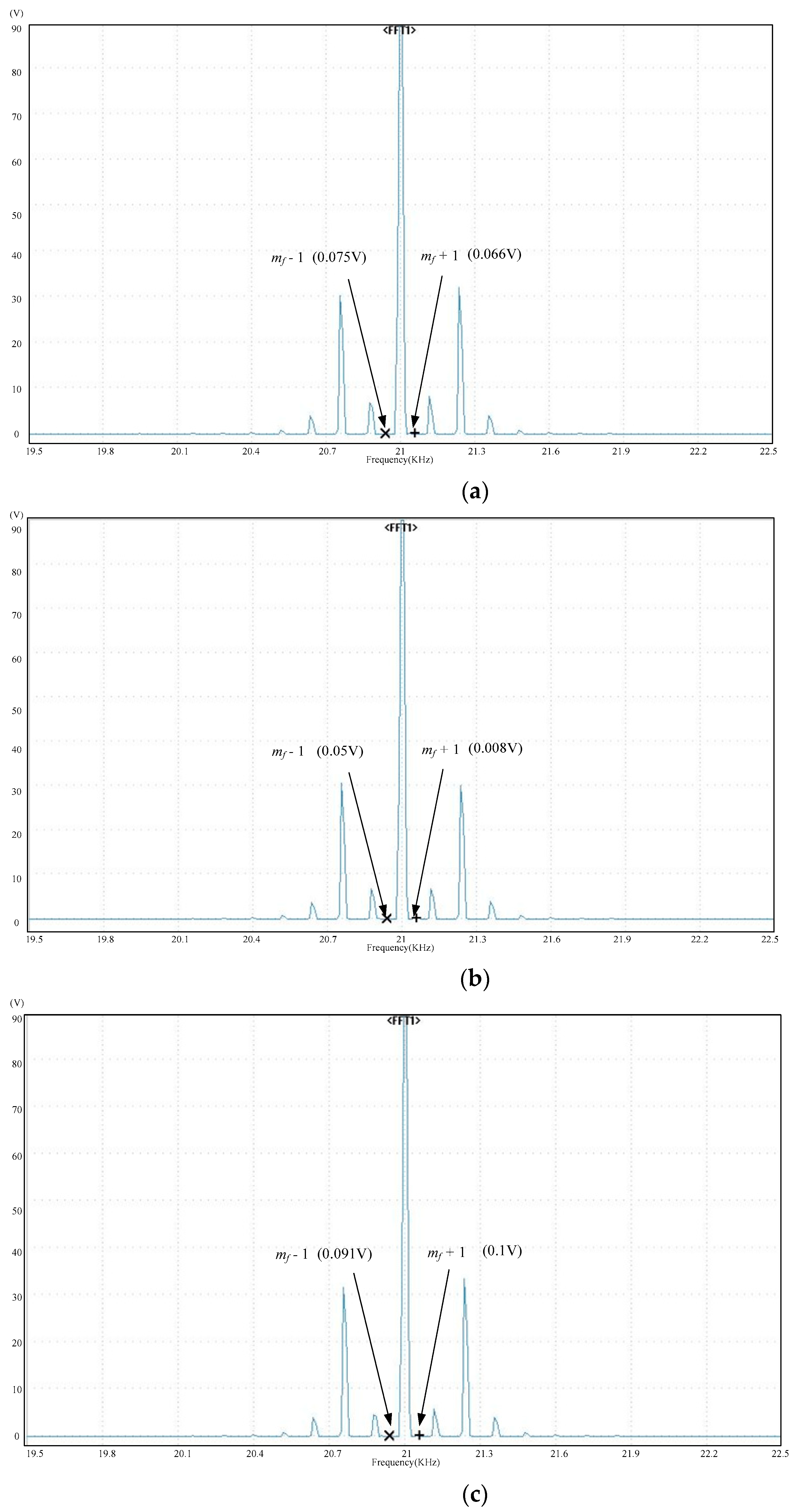
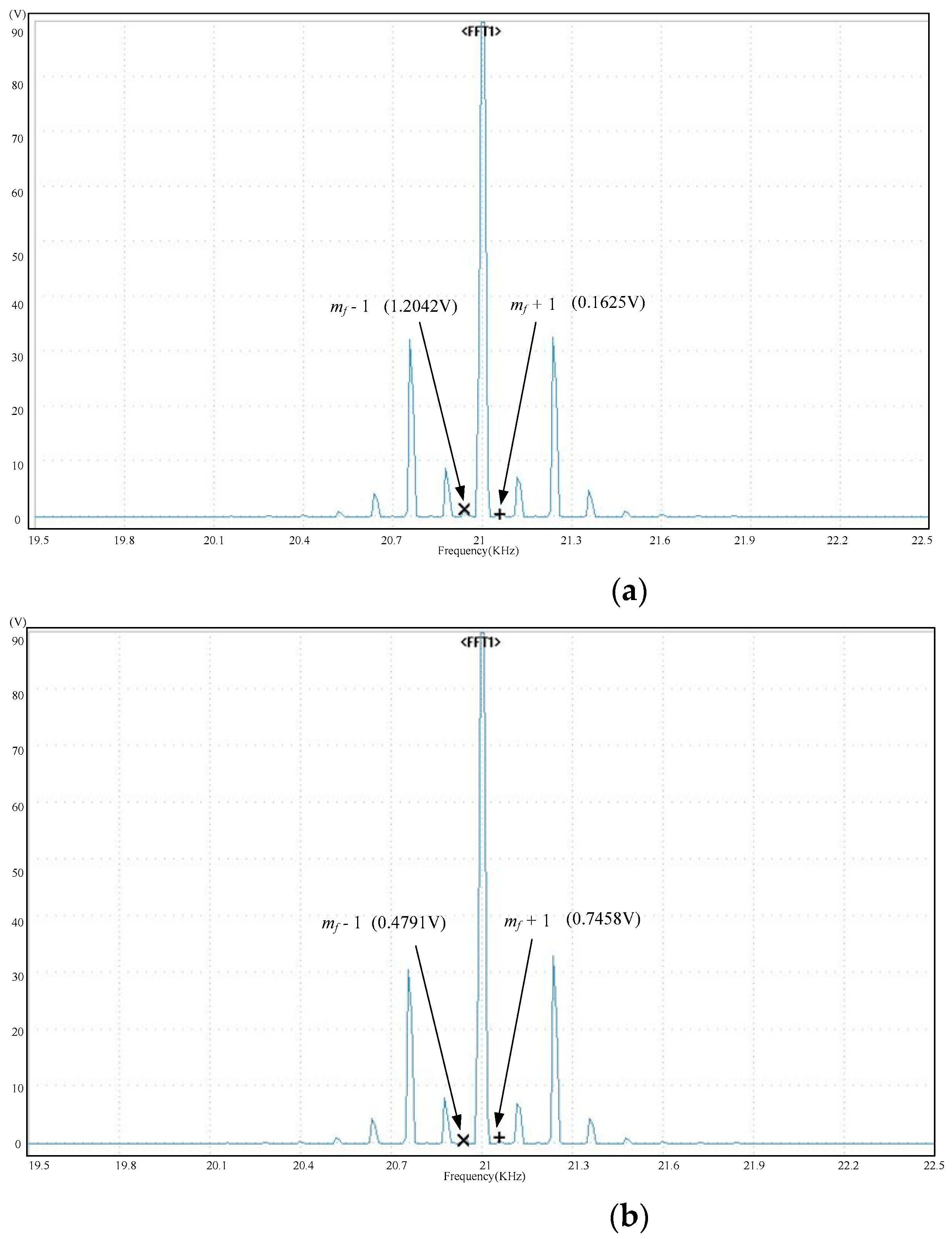
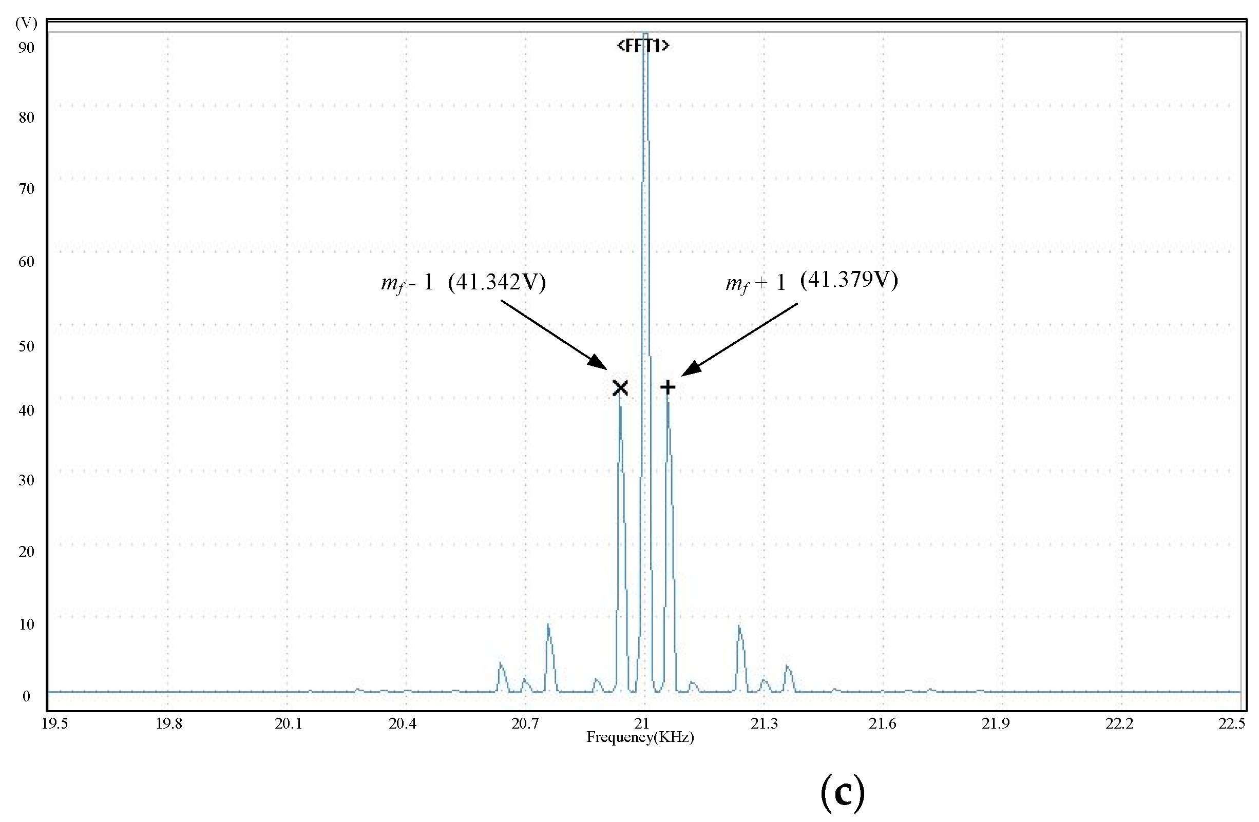
5. Test Results

To detect faulty power transistors, the fault categories were divided into the fault of six switches, specifically, Sa1+, Sa2, Sb1+, Sb2, Sc1+, and Sc2 (Table 1).
The characteristic spectral data of the various phase voltages of the inverter operating at 52 Hz, 85 Hz, and 120 Hz with a fault in each of the switches are tabulated in Table 2, Table 3 and Table 4, respectively. The test data in Table 2, Table 3 and Table 4 were incorporated into the proposed fault diagnosis system.
The detection outcomes are tabulated in Table 5, Table 6 and Table 7. The tables show that the system accurately detected the fault data. For example, the detection outcomes in Table 5 generated an output weight of 0.6999 for the test data of F2 faults in Table 2, which was the highest of all the fault data points, suggesting that the fault was category F2. To validate the interference resistance of the proposed system, the samples for three working frequencies were tested with an error margin of ± 5 % . The detection outcomes are tabulated in Table 8, Table 9 and Table 10. The outcomes show that the proposed system can accurately detect fault categories with or without the presence of error.
In the half-bridge and full-bridge circuits, where two transistors are connected in series in one converter leg, it is important to provide a blanking time so that the turn-on control input to one transistor is delayed with respect to turn-off control input of the other transistor in the inverter leg. This blanking time should be chosen conservatively to be greater than the worst-case maximum storage time of the transistors being used to avoid cross condition. Under normal operation, such a conservatively chosen blanking time ensures that both the transistors in the inverter leg are off. This dead time introduces an unwanted nonlinearity in the converter transfer characteristic. This dead time can be minimized by the use of design enhancements to drive circuits, which minimize turn-on and turn-off delay time in power semiconductor devices being used as the power switches. There are usually only a few us for a power device IGBT. Therefore, its influence on fault diagnosis can be ignored.

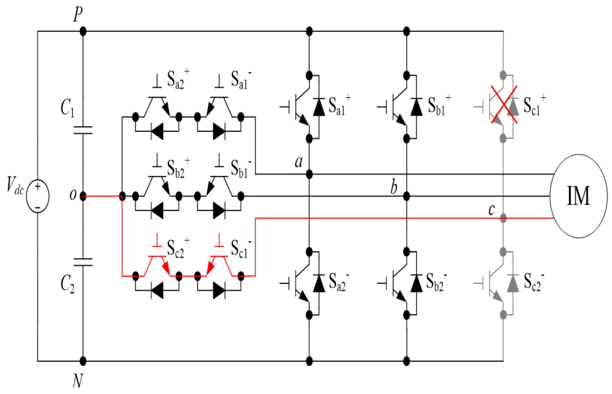
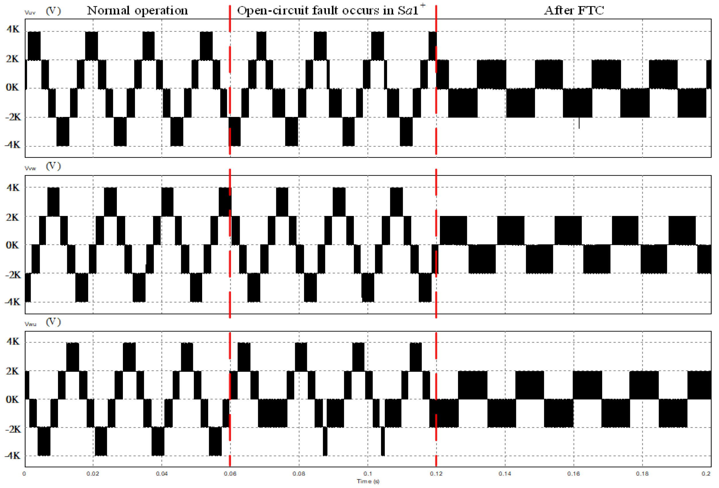
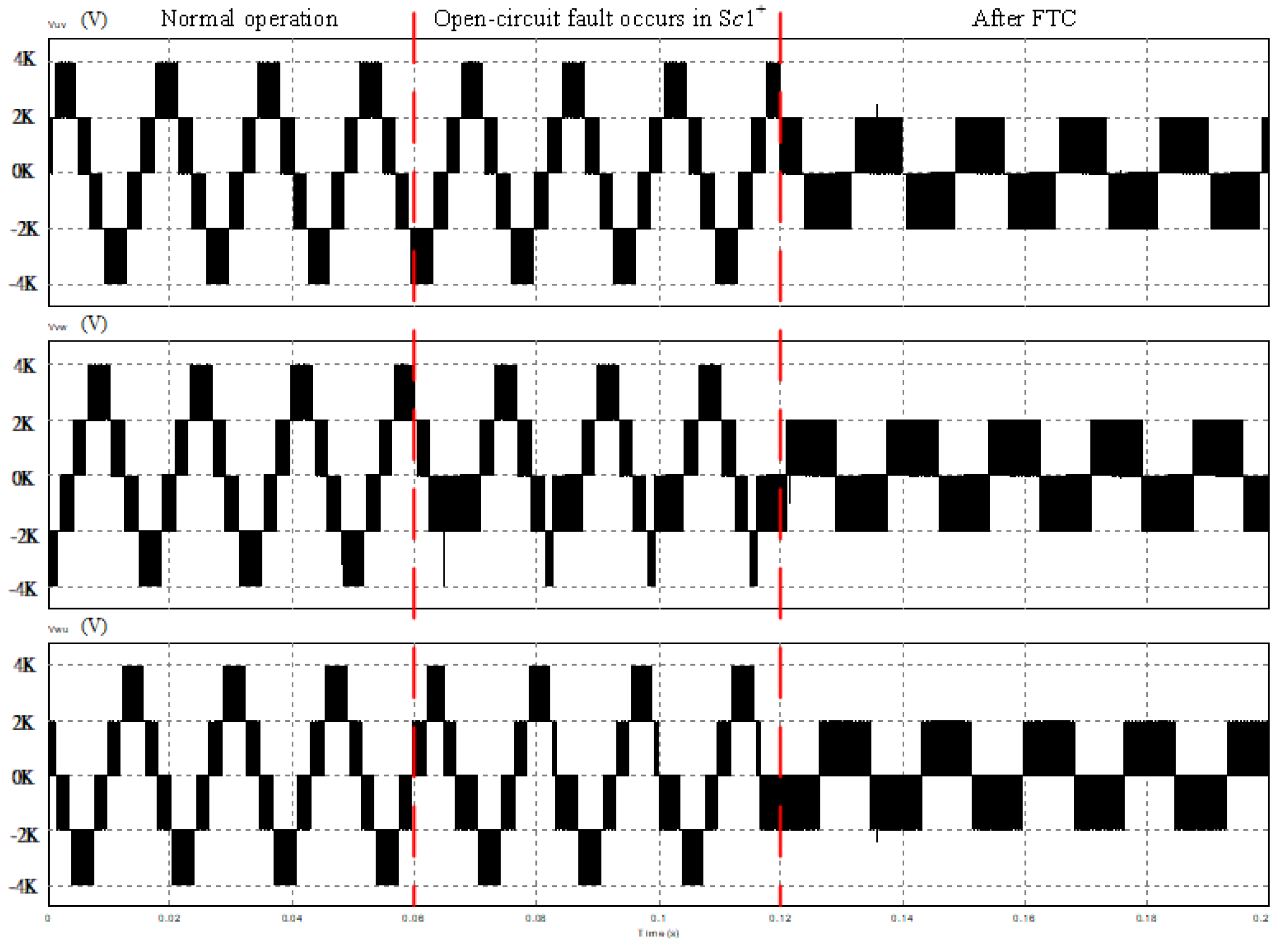
6. Fault Tolerance of Three-Level T-Type Inverter

Figure 2 presents the structural diagram of the three-level T-type inverter, revealing that the occurrence of an open-circuit fault in any of the inverter switches (Sa1+, Sa2, Sb1+, Sb2, Sc1+, and Sc2) would cause an abnormal output voltage in the phase and thus result in a three-phase imbalance. The imbalance would change the voltage level of the dc bus, engendering a voltage imbalance in the upper and lower capacitors. This situation would further induce repeated three-phase imbalances in the output voltage. Therefore, to maintain inverter operation in the event of switch failure, the switching state of the inverter and the phase angle of the reference voltage must be adjusted simultaneously to maintain the three-phase balance in the output voltage.

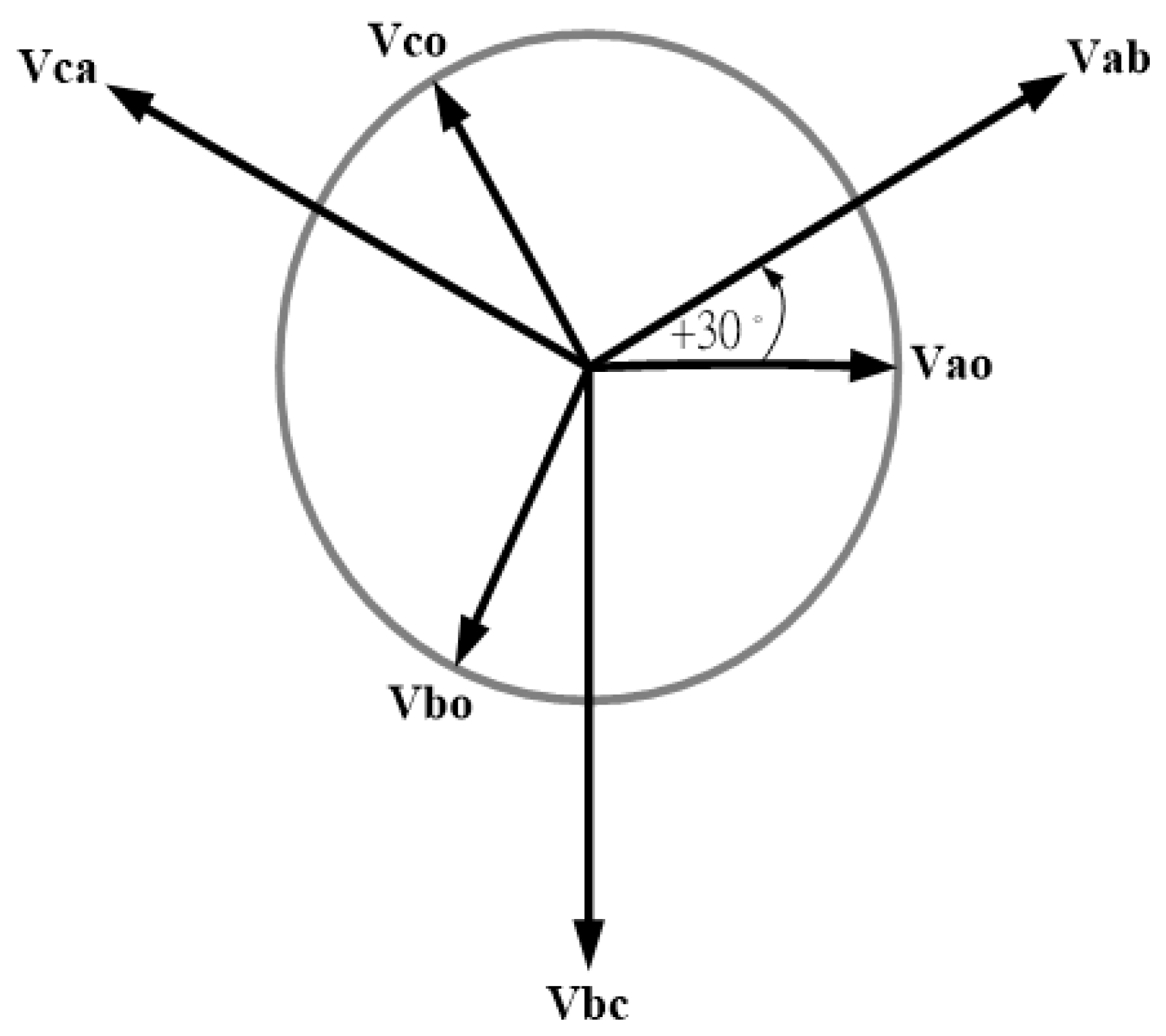
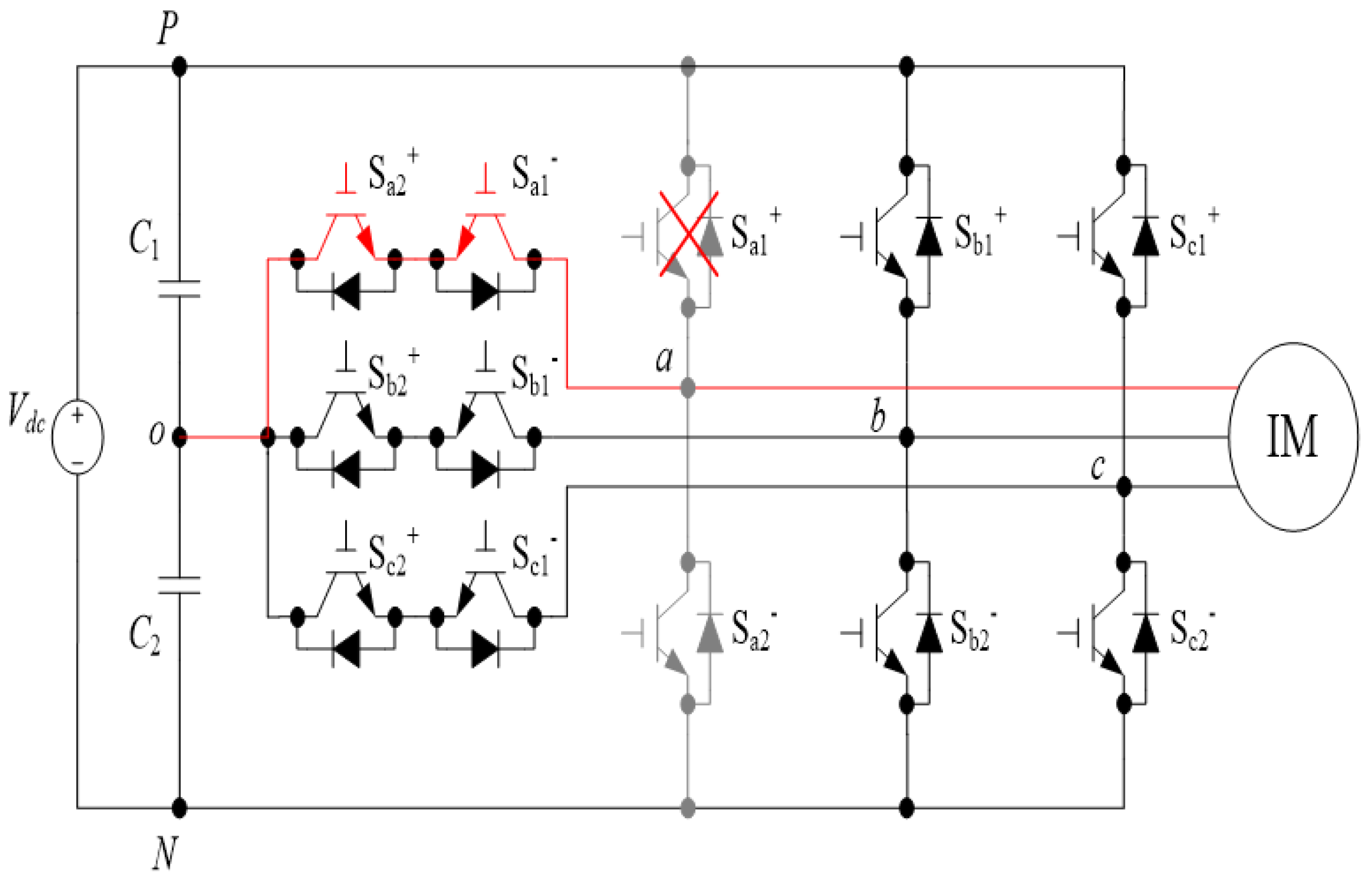
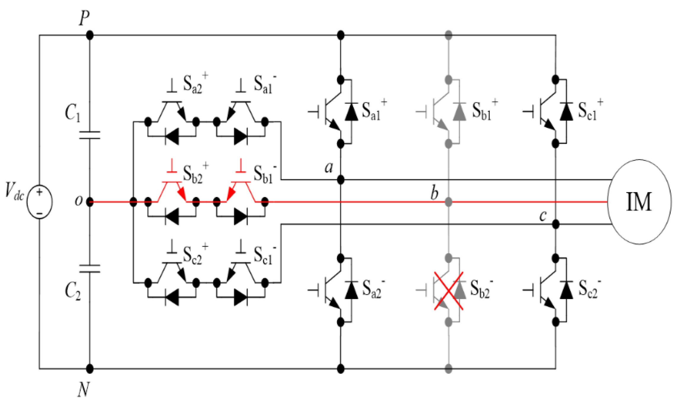
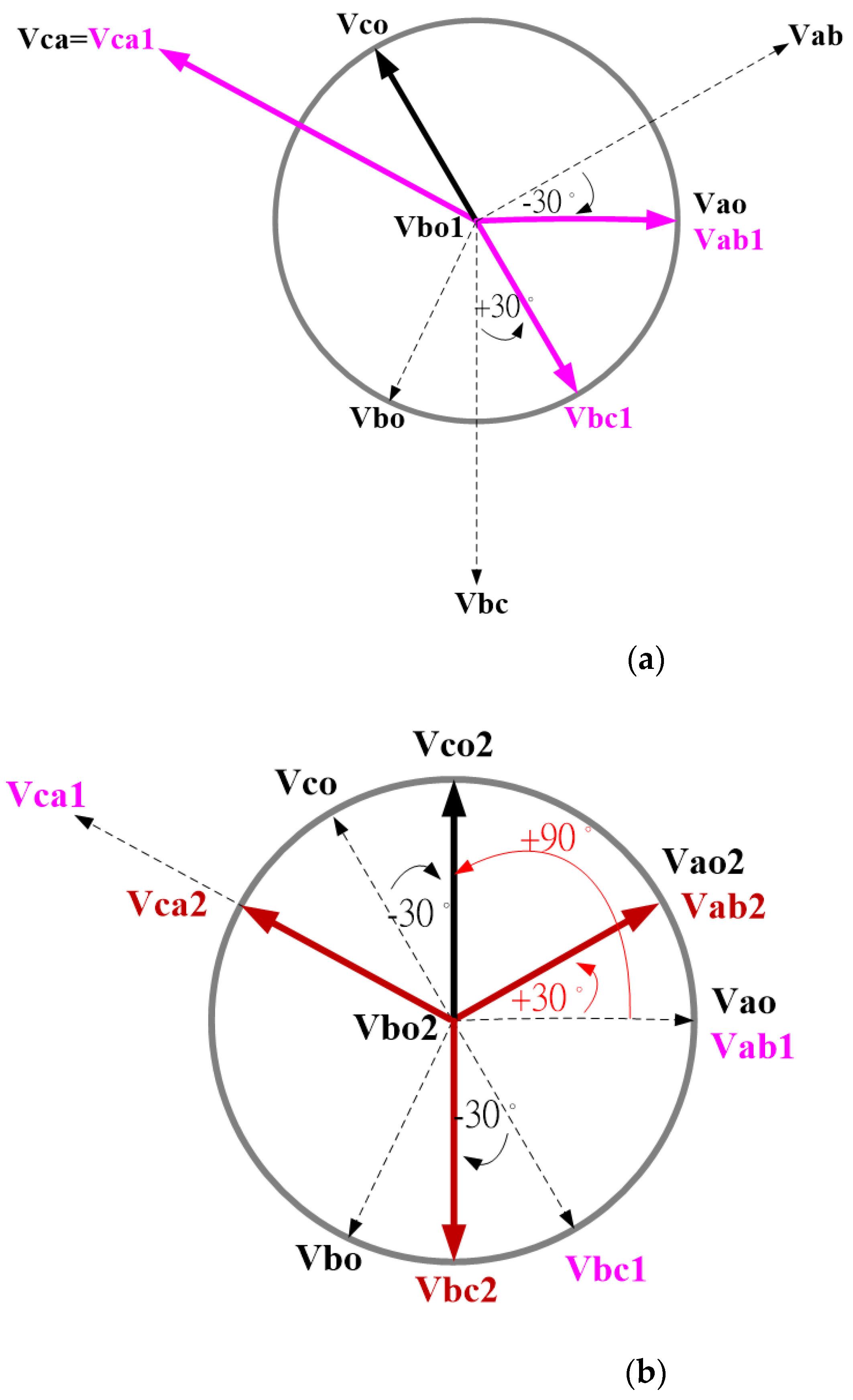
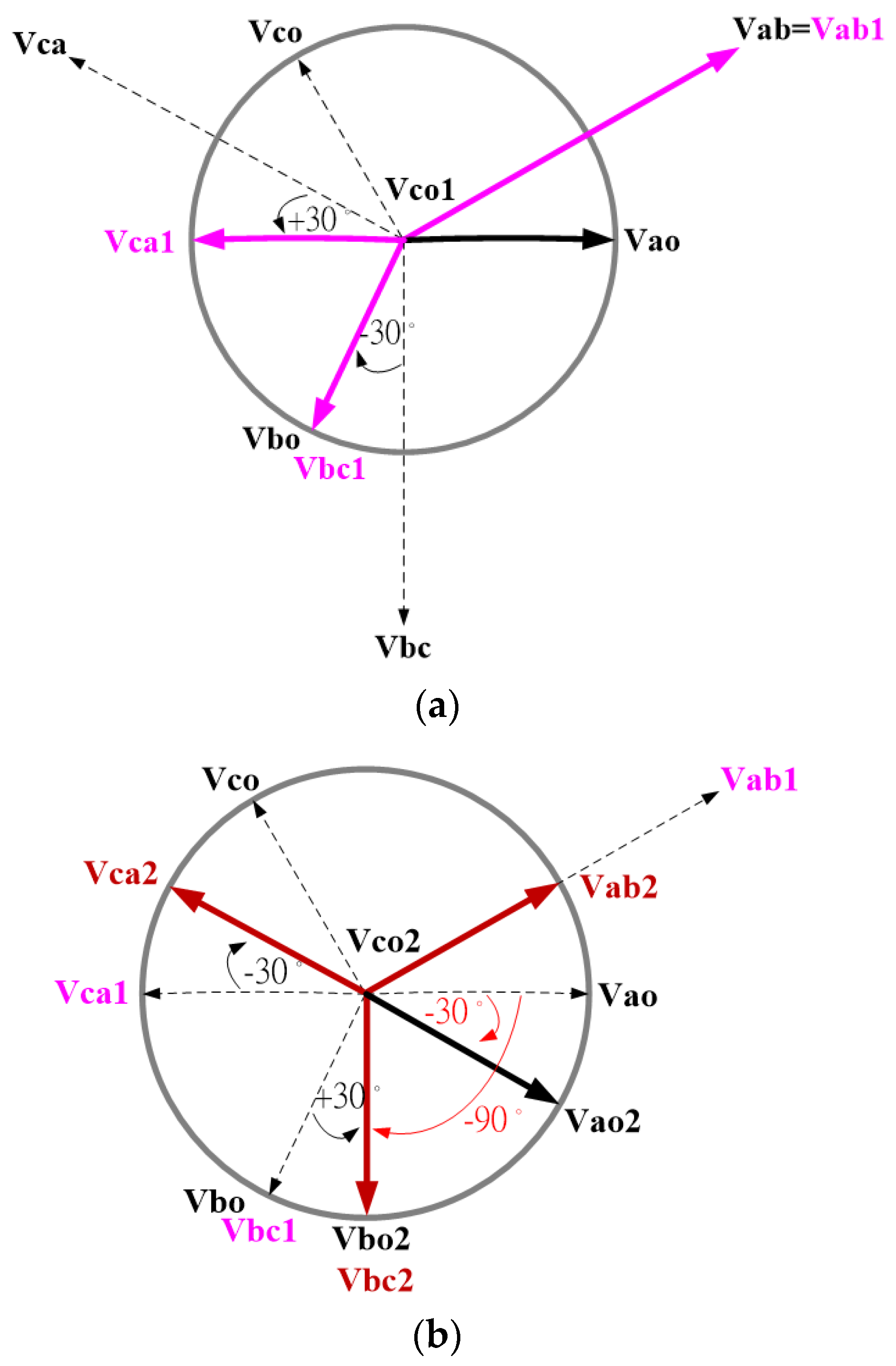
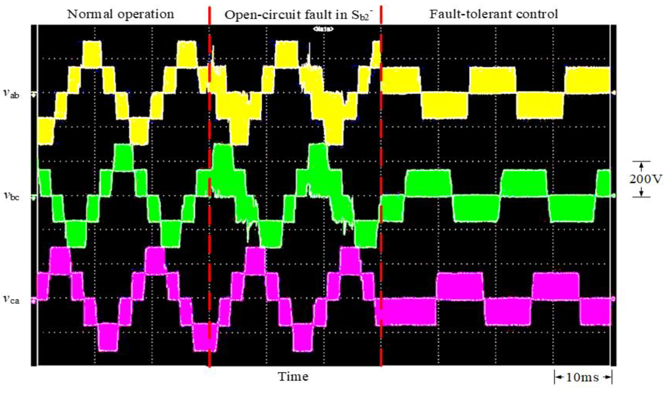
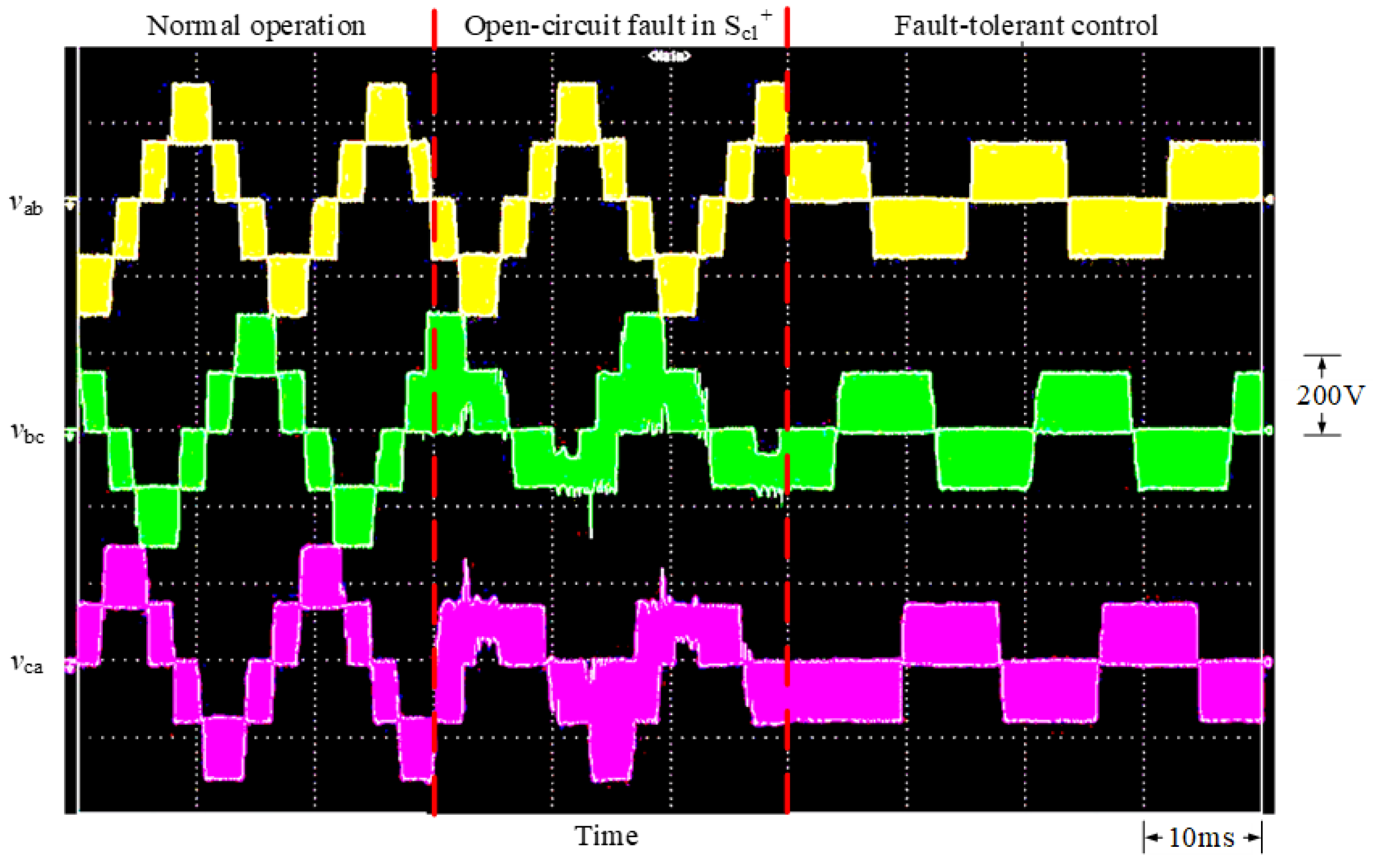
6.1. Fault-Tolerant Control Analysis

Figure 12 shows the phasor diagram of a balanced three-phase voltage of a switch without fault. When the switch Sa1+ or Sa2 incurs an open-circuit fault, the a-phase h-bridge switches (Sa1+ and Sa2) must be deactivated to activate the neutral-point switches (Sa1 and Sa2+); specifically, point a is connected to the neutral point, and b and c-phases are still switched normally. The FTC for the occurrence of an open-circuit fault in Sa1+ is shown in Figure 13. The voltage phasor diagram corresponding to this situation is illustrated in Figure 14a. As illustrated in this figure, the phasor positions of the line voltages Vab and Vca in Figure 12 become those of Vab1 and Vca1, with the voltage magnitude decreasing by 0.577 times relative to the original line voltage. The line voltage Vbc1 remains unchanged. However, because the voltage vao is 0, the phase angle of the b-phase voltage should be simultaneously adjusted to be 150° behind that of the a-phase voltage, and the phase angle of the c-phase voltage should be 150° ahead of that of the a-phase voltage. After the occurrence of a fault, the three-phase voltage can still maintain the operation of the balanced three-phase system; the corresponding voltage phasor diagram of the system is shown in Figure 14b. The phasor positions of the line voltages Vab1 and Vca1 presented in Figure 14a shift to those of Vab2 and Vca2, with the magnitude of the line voltage Vbc2 decreasing by 0.577 times relative to that of the original line voltage Vbc1. If an open-circuit fault occurs in the switch Sb1+ or Sb2, the b-phase h-bridge switches (Sb1+ and Sb2) are deactivated, and the neutral-point switches (Sb1 and Sb2+) are activated; specifically, point b is connected to the neutral point, and the a- and c-phase switches continue to operate normally. The FTC for the occurrence of an open-circuit fault in Sb2 is shown in Figure 15. The voltage phasor diagram corresponding to this situation is shown in Figure 16a. The phasor positions of the line voltages Vab and Vbc in Figure 12 shift to those of Vab1 and Vbc1, with the voltage magnitude decreasing by 0.577 times relative to the magnitude of the original line voltage; by contrast, the magnitude of the line voltage Vca1 remains unchanged. However, because the voltage vbo is 0, the phase angle of the a-phase voltage should be simultaneously adjusted such that it is 30° ahead of that of the a-phase voltage, and the phase angle of the c-phase voltage should be 90° ahead of that of the a-phase voltage. Figure 16b presents the voltage phasor diagram derived after these adjustments. The phasor positions of the line voltages Vab1 and Vbc1 presented in Figure 16a shift to those of Vab2 and Vbc2, with the magnitude of the line voltage Vca2 decreasing by 0.577 times relative to that of the original line voltage Vca1. Similarly, if an open-circuit fault occurs in the switch Sc1+ or Sc2, the c-phase h-bridge switches (Sc1+ and Sc2) are deactivated, and the neutral-point switches (Sc1 and Sc2+) are activated. Point c is connected to the neutral point, and the a- and b-phase switches continue to operate normally. The FTC for the occurrence of an open-circuit fault in Sc1+ is shown in Figure 17. Figure 18a shows the voltage phasor diagram corresponding to this situation. The phasor positions of the line voltages Vbc and Vca shown in Figure 12 switch to those of Vbc1 and Vca1, with the voltage magnitude decreasing by 0.577 times relative to the magnitude of the original line voltage; by contrast, the magnitude of the line voltage Vab1 remains unchanged. However, because the voltage vco is 0, the phase angle of the a-phase voltage should be simultaneously adjusted such that it is 30° behind the original a-phase voltage, and the phase angle of the b-phase voltage should be 90° behind the original a-phase voltage. Figure 18b illustrates the voltage phasor diagram derived after the adjustments. The phasor positions of the line voltages Vbc1 and Vca1 presented in Figure 18a switch to the positions of Vbc2 and Vca2, with the magnitude of Vab2 decreasing by 0.577 times relative to that of the original line voltage Vab1.

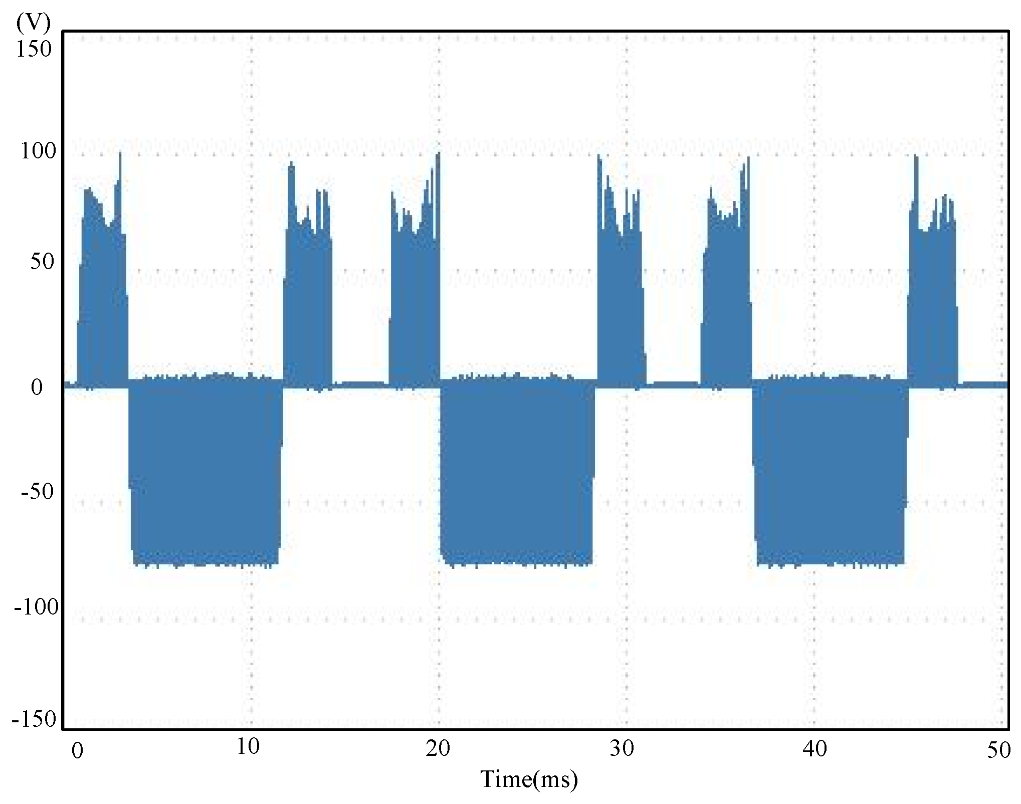
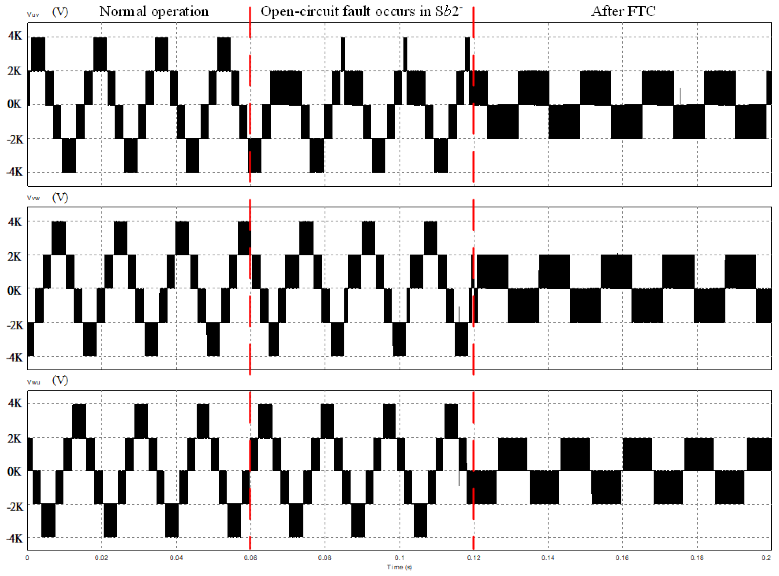
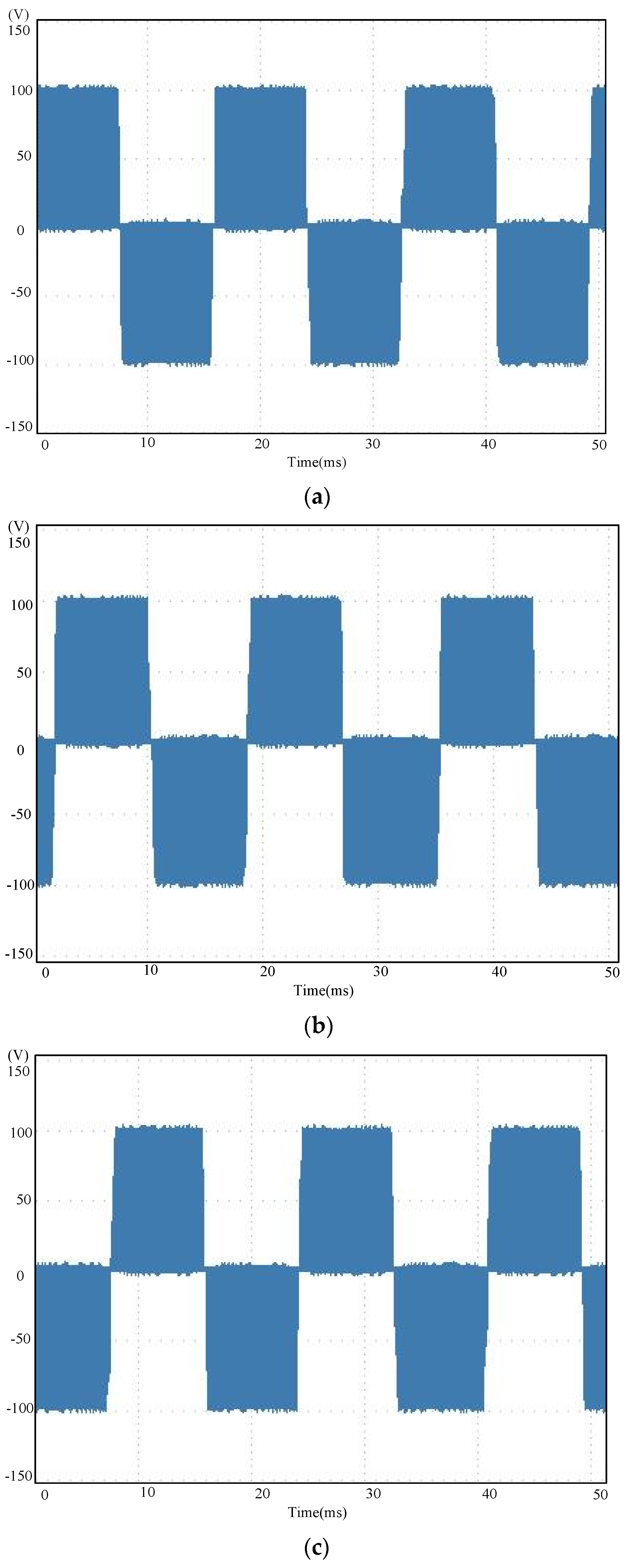
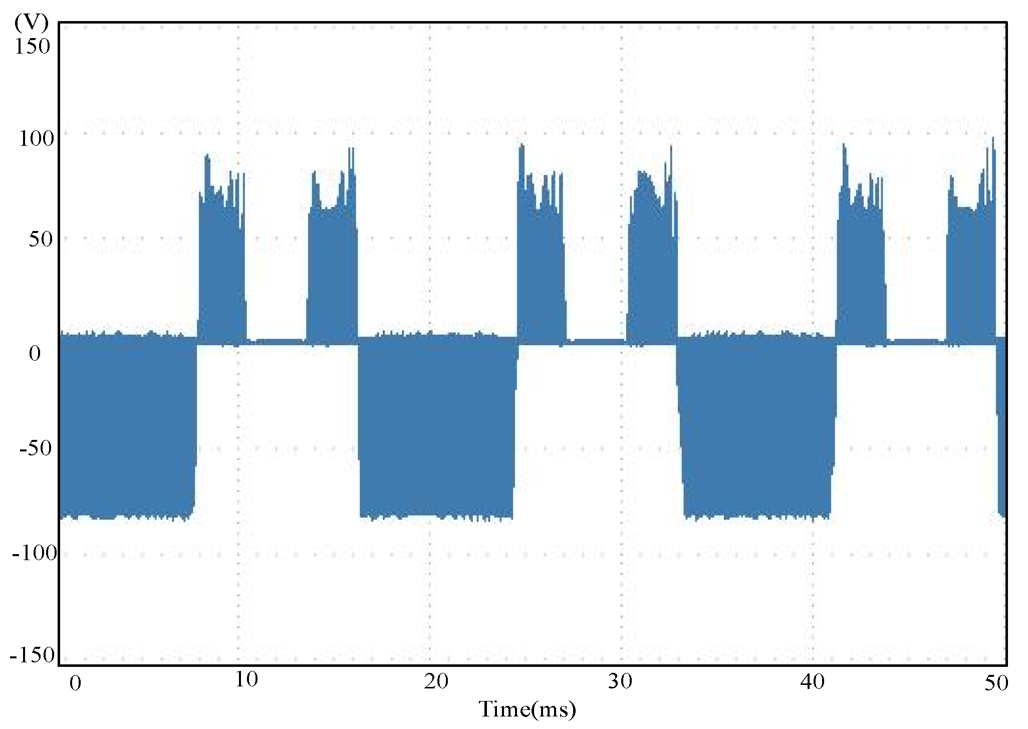
6.2. FTC Simulation Results

The FTC operations for the occurrence of an open-circuit fault in Sa1+, Sb2, and Sc1+ were simulated. The simulation results are illustrated in Figure 19, Figure 20 and Figure 21. Distortion was exhibited in the three-phase output line voltage 0.06 s following the occurrence of an open-circuit fault, particularly in the faulty phase. The FTC was activated at 0.12 s. The figures show that once the FTC was activated, the five-level three-phase output line voltage was reduced to three levels and the output line voltage maintained three-phase balance after the occurrence of a fault.

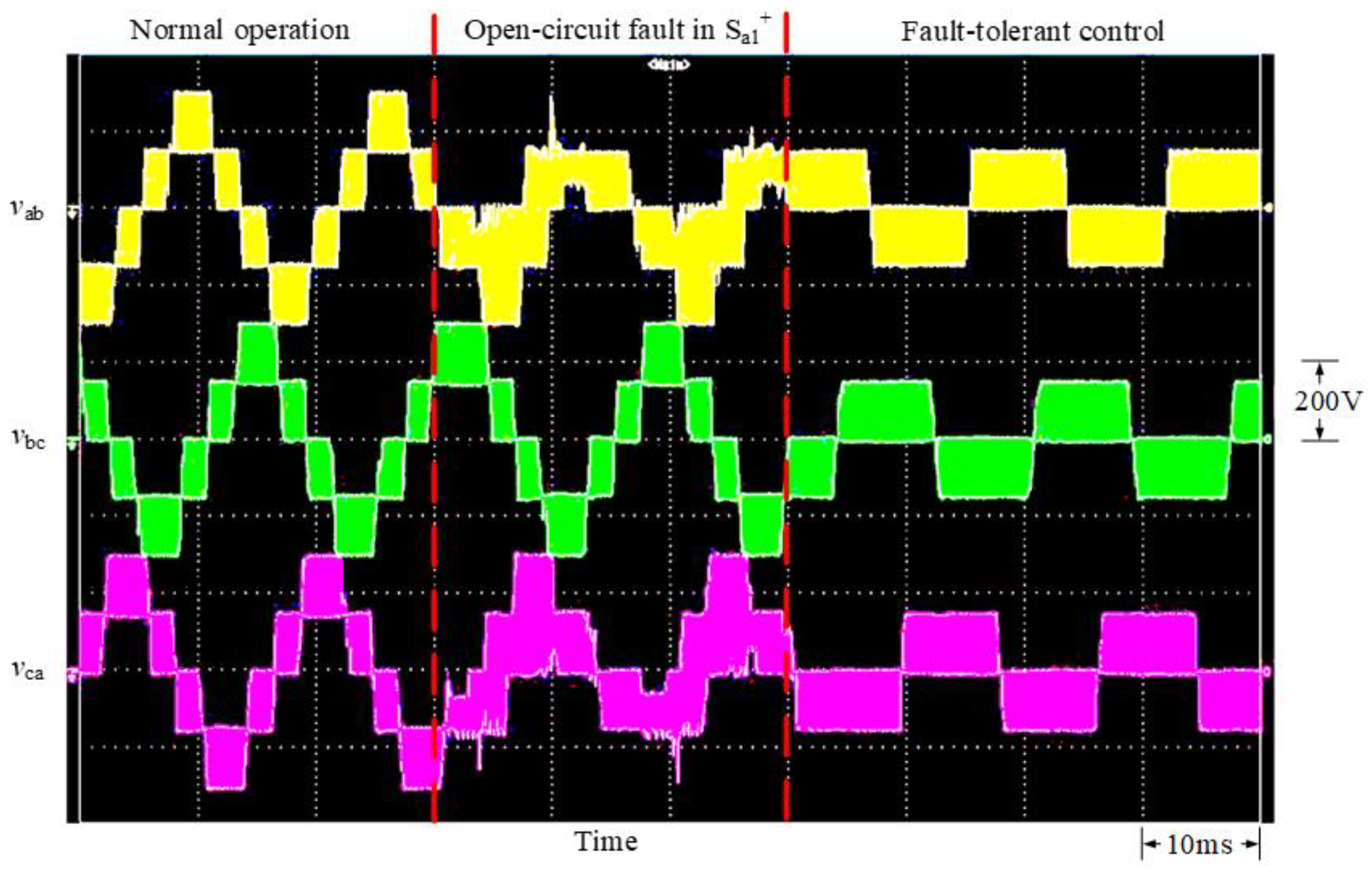
6.3. FTC Experimental Results

To verify the simulation results, this study uses the digital signal processor TMS320F28335 as the control core and considers the occurrence of open-circuit faults in the switches Sa1+, Sb2, and Sc1+ to test the fault-tolerant control strategy. Regarding the parameter setting of the motor drive, a 300-Vdc inverter with a switching frequency of 21 kHz is connected to an induction motor. The parameters of the induction motor are listed in Table 11.
Figure 22 shows that the occurrence of an open-circuit fault in the switch Sa1+ would distort the three-phase output line voltage. The fault is particularly severe in the vab and vca phases, and the fault-tolerant control strategy can be launched 0.03 s after the occurrence of the fault. In this situation, the a-phase h-bridge switches (Sa1+ and Sa2) are deactivated, and the neutral-point switches (Sa1 and Sa2+) are thus activated. The b and c-phase switches still operate normally; the phase angle of the b-phase voltage is simultaneously adjusted such that it is 150° behind the phase angle of the a-phase reference voltage, and the phase angle of the c-phase reference voltage is adjusted such that it is 150° ahead of that of the a-phase voltage. After the execution of the fault-tolerant control strategy, the three-phase output line voltage is reduced from five to three levels (Figure 22). However, after the occurrence of the fault, the output line voltage still maintains the operation of the balanced three-phase system. Therefore, the motor can still operate normally under reduced load.
If an open-circuit fault occurs in the switch Sb2, the fault would distort the three-phase output line voltage, as illustrated in Figure 23. The fault is particularly severe in the vab and vbc phases. In this situation, if the fault-tolerant control strategy is launched, the b-phase h-bridge switches (Sb1+ and Sb2) are deactivated and the neutral-point switches (Sb1 and Sb2+) are thus activated; the a- and c-phase switches still operate normally. However, the phase angle of the new a-phase reference voltage is adjusted such that it is 30° ahead of that of the original a-phase reference voltage, and the phase angle of the c-phase reference voltage is adjusted such that it is 90° ahead of that of the original a-phase voltage. Figure 23 indicates that after the execution of the fault-tolerant control strategy, the three-phase output line voltage is reduced from five to three levels; however, after the occurrence of the fault, the output line voltage can maintain the operation of the balanced three-phase system. Therefore, the motor can continue to operate appropriately under reduced load.
If an open-circuit fault occurs in the switch Sc1+, the fault would distort the three-phase output line voltage, as presented in Figure 24. The fault is particularly severe in the vbc and vca phases. If the fault-tolerant control is launched 0.03 s after the occurrence of the fault, the c-phase h-bridge switches (Sc1+ and Sc2) are deactivated and the neutral-point switches (Sc1 and Sc2+) are activated; the a- and b-phase switches still operate normally. The phase angle of the a-phase reference voltage is adjusted such that it is 30° behind that of the original a-phase reference voltage, and the phase angle of the b-phase reference voltage is adjusted such that it is 90° behind that of the original a-phase reference voltage. Figure 24 reveals that after the execution of the fault-tolerant control strategy, the three-phase output line voltage is also reduced from five to three levels. However, after the occurrence of the fault, the output line voltage can maintain the operation of the balanced three-phase system. Therefore, the motor can continue to operate appropriately under reduced load.
If the capacitor at the DC link is not large enough, and the switching of FTC is not fast enough, the voltage of DC link will vary. In this paper, because the capacitor used in the DC link is quite large, and the switching time of FTC switch is very short, there is almost no voltage variation in the DC link before fault and after clearing the fault.

7. Conclusions

This paper proposed a CMAC-based fault diagnosis system for inverters capable of detecting the positions of faulty power transistors in three-level T-type inverters. The application of a CMAC reduces training time. It also possesses capabilities to reduce the effects of interference signals. The FTC strategy enabled the system to engage in FTC immediately following the occurrence of a fault to maintain the normal supply power of the inverter, thereby greatly enhancing the power reliability of three-level T-type inverters. Finally, the experimental results verify that the proposed system can accurately detect fault categories, even with the presence of interference. Moreover, the FTC strategy enables the system to maintain the three-phase balance of the output line voltage upon the occurrence of a switch fault, confirming the feasibility of the proposed system.

Author Contributions

K.-H.C. planned the project and did the writing, editing, and review. He also did the analysis and optimized the cerebellar model articulation controller. L.-Y.C. developed the three-level T-type inverter and used to create a three-level T-type inverter test environment. C.-C.H. was responsible for data curation, software and experimental corroboration for the T-type inverter and fault-tolerant controller. K.-H.C. administered the project. All authors have read and agreed to the published version of the manuscript.

Funding

The authors gratefully acknowledge the support and funding of this paper by the Ministry of Science and Technology, Taiwan, under the Grant Number MOST 109-2221-E-167-016-MY2.

Conflicts of Interest

The authors declare no conflict of interest.

References

  1. Rodriguez, J.I.; Leeb, S.B. A Multilevel inverter topology for inductively coupled power transfer. IEEE Trans. Power Electron. 2006, 21, 1607–1617. [Google Scholar] [CrossRef]
  2. Escalante, M.F.; Vannier, J.C.; Arzande, A. Flying capacitor multilevel inverters and DTC motor drive applications. IEEE Trans. Ind. Electron. 2002, 49, 809–815. [Google Scholar] [CrossRef]
  3. Tourkhani, F.; Viarouge, P.; Meynard, T.A. Optimal design and experimental results of a multilevel inverter for an UPS application. In Proceedings of the Second International Conference on Power Electronics and Drive Systems, Singapore, 26–29 May 1997; pp. 340–343. [Google Scholar]
  4. Daher, S.; Schmid, J.; Antunes, F.L.M. Multilevel inverter topologies for stand-alone PV systems. IEEE Trans. Ind. Electron. 2008, 55, 2703–2712. [Google Scholar] [CrossRef]
  5. Naik, R.L.; Udaya, K.R.Y. A novel technique for control of cascaded multilevel inverter for photovoltaic power supplies. In Proceedings of the 2005 European Conference on Power Electronics and Applications, Dresden, Germany, 11–14 September 2005; pp. 1–9. [Google Scholar]
  6. Nabae, A.; Takahashi, I.; Akagi, H. A new neutral-point clamped PWM inverter. IEEE Trans. Ind. Appl. 1981, 17, 518–523. [Google Scholar] [CrossRef]
  7. Schweizer, M.; Kolar, J.W. Design and implementation of a highly efficient three-level T-type converter for low-voltage applications. IEEE Trans. Power Electron. 2013, 28, 899–907. [Google Scholar] [CrossRef]
  8. Chen, A.; Hu, L.; Chen, L.; Deng, Y.; Yao, G.; He, X. A multilevel converter topology with fault-tolerant ability. IEEE Trans. Power Electron. 2005, 20, 405–415. [Google Scholar] [CrossRef]
  9. Khomfoi, S.; Tolbert, L.M. Fault diagnostic system for a multilevel inverter using a neural network. IEEE Trans. Power Electron. 2007, 22, 1062–1069. [Google Scholar] [CrossRef]
  10. Choi, U.; Lee, K.; Blaabjerg, F. Diagnosis and tolerant strategy of an open-switch fault for T-type three-level inverter systems. IEEE Trans. Ind. Appl. 2014, 50, 495–508. [Google Scholar] [CrossRef]
  11. Chao, A.M. Motor Fault Diagnosis by Using Fuzzy Neural Network. Master’s Thesis, Chung Yuan Christian University, Taoyuan, Taiwan, 2004. [Google Scholar]
  12. Ahmadi, S.; Poure, P.; Saadate, S.; Khaburi, D.A. Fault tolerance analysis of five-level neutral-point-clamped inverters under clamping diode open-circuit failure. Electronics 2022, 11, 1461. [Google Scholar] [CrossRef]
  13. Chao, K.H.; Ke, C.H. Fault diagnosis and tolerant control of three-level neutral-point clamped inverters in motor drives. Energies 2020, 13, 6302. [Google Scholar] [CrossRef]
  14. Han, T.; Yang, B.S.; Lee, J.M. A new condition monitoring and fault diagnosis system of induction motors using artificial intelligence algorithms. In Proceedings of the IEEE International Conference on Electrical Machines and Drives, San Antonio, TX, USA, 15 May 2005; pp. 1967–1974. [Google Scholar]
  15. Chen, T.; Pan, Y.; Xiong, Z. A hybrid system model-based open-circuit fault diagnosis method of three-phase voltage-source inverters for PMSM drive systems. Electronics 2020, 9, 1251. [Google Scholar] [CrossRef]
  16. Lehtoranta, J.; Koivo, H.N. Fault diagnosis of induction motors with dynamical neural networks. In Proceedings of the IEEE International Conference on System, Man and Cybernetics, Waikoloa, HI, USA, 12 October 2005; pp. 2979–2984. [Google Scholar]
  17. He, Q.; Du, D.M. Fault diagnosis of induction motor using neural networks. In Proceedings of the International Conference on Machine Learning and Cybernetics, Hong Kong, China, 19–22 August 2007; pp. 1090–1095. [Google Scholar]
  18. Murphey, Y.L.; Masrur, M.A.; Chen, Z.H.; Zhang, B. Model-based fault diagnosis in electric drives using machine learning. IEEE/ASME Trans. Mechatron. 2006, 11, 290–303. [Google Scholar] [CrossRef]
  19. Zidani, F.; Benbouzid, M.E.H.; Diallo, D.; Nait-Said, M.S. Induction motor stator faults diagnosis by a current concordia pattern based fuzzy decision system. IEEE Trans. Energy Convers. 2003, 18, 469–475. [Google Scholar] [CrossRef] [Green Version]
  20. Nejjari, H.; Benbouzid, M.E.H. Monitoring and diagnosis of induction motors electrical faults using a current Park’s vector pattern learning approach. IEEE Trans. Ind. Appl. 2000, 36, 730–735. [Google Scholar] [CrossRef]
  21. Diallo, D.; Benbouzid, M.E.H.; Hamad, D.; Pierre, X. Fault detection and diagnosis in an induction machine drive: A pattern recognition approach based on concordia stator mean current vector. IEEE Trans. Energy. Convers. 2005, 20, 512–519. [Google Scholar] [CrossRef] [Green Version]
  22. Zidani, F.; Diallo, D.; Benbouzid, M.E.H.; Nait-Said, R. A Fuzzy-based approach for the diagnosis of fault modes in a voltage-fed PWM inverter induction motor drive. IEEE Trans. Ind. Electron. 2008, 55, 586–593. [Google Scholar] [CrossRef] [Green Version]
  23. Zhang, K.; Jiang, B.; Staroswiecki, M. Dynamic output feedback fault tolerant controller design for Takagi-Sugeno fuzzy systems with actuator faults. IEEE Trans. Fuzzy Syst. 2010, 18, 194–201. [Google Scholar] [CrossRef]
  24. Awadallah, M.A.; Morcos, M.M. Diagnosis of switch open-circuit fault in PM brushless DC motor drives. In Proceedings of the Power Engineering Conference on Large Engineering System, Montreal, QC, Canada, 7–9 May 2003; pp. 69–73. [Google Scholar]
  25. Albus, J.S. A new approach to manipulator control: The cerebellar model articulation controller. Trans. ASME J. Dynam. Syst. Meas. Contr. 1975, 97, 220–227. [Google Scholar] [CrossRef] [Green Version]
  26. Hung, C.P.; Chao, K.H. CMAC neural network application on lead-acid batteries residual capacity estimation. In Proceedings of the 3th International Conference on Intelligent Computing, Qingdao, China, 21–24 August 2007; pp. 961–970. [Google Scholar]
  27. Handeiman, D.A.; Lane, S.H.; Gelfand, J.J. Integrating neural networks and knowledge-based systems for intelligent robotic control. IEEE Contr. Syst. Mag. 1990, 10, 77–87. [Google Scholar] [CrossRef]
Figure 1. The CMAC-based fault diagnosis system for inverter architecture.
Electronics 11 02496 g001
Figure 2. The three-level T-type inverter architecture.
Electronics 11 02496 g002
Figure 3. The time command PWM generation scheme of switches for a three-level T-type inverter.
Electronics 11 02496 g003
Figure 4. Output voltage waveforms of the inverter at a working frequency of 60 Hz with no switch faults: (a) phase voltage vao; (b) phase voltage vbo; (c) phase voltage vco.
Electronics 11 02496 g004
Figure 5. The frequency spectra of the various phase voltages of the inverter at a working frequency of 60 Hz with no switch faults: (a) phase voltage vao; (b) phase voltage vbo; (c) phase voltage vco.
Electronics 11 02496 g005
Figure 6. Waveform of the a-phase output voltage (vao) of the inverter at a working frequency of 60 Hz with a fault in switch Sa1+.
Electronics 11 02496 g006
Figure 7. Waveform of the b-phase output voltage (vbo) of the inverter at a working frequency of 60 Hz with a fault in switch Sb2.
Electronics 11 02496 g007
Figure 8. Waveform of the c-phase output voltage (vco) of the inverter at a working frequency of 60 Hz with a fault in switch Sc1+.
Electronics 11 02496 g008
Figure 9. The frequency spectra of the various phase voltages of the inverter at a working frequency of 60 Hz with a fault in switch Sc1+: (a) phase voltage vao; (b) phase voltage vbo; (c) phase voltage vco.
Electronics 11 02496 g009aElectronics 11 02496 g009b
Figure 10. CMAC framework.
Electronics 11 02496 g010
Figure 11. Training flowchart for the CMAC-based fault diagnosis system for inverters.
Electronics 11 02496 g011
Figure 12. Balanced three-phase voltage phasor diagram of a switch without fault.
Electronics 11 02496 g012
Figure 13. FTC for the occurrence of an open-circuit fault in Sa1+.
Electronics 11 02496 g013
Figure 14. Voltage phasor diagram of fault-tolerant control when a fault occurs in the switch Sa1+ or Sa2; (a) unadjusted voltage phase angle; (b) adjusted phase angle of the b-phase voltage such that it is 150° behind that of the a-phase voltage; adjusted phase angle of the c-phase voltage such that it is 150° ahead of that of the a-phase voltage.
Electronics 11 02496 g014
Figure 15. FTC for the occurrence of an open-circuit fault in Sb2.
Electronics 11 02496 g015
Figure 16. Voltage phasor diagram of fault-tolerant control when a fault occurs in the switch Sb1+ or Sb2; (a) unadjusted voltage phase angle; (b) adjusted phase angle of the a-phase voltage such that it is 30° ahead of the original phase angle of the a-phase voltage; adjusted phase angle of the c-phase voltage such that it is 90° ahead of the original phase angle of the a-phase voltage.
Electronics 11 02496 g016
Figure 17. FTC for the occurrence of an open-circuit fault in Sc1+.
Electronics 11 02496 g017
Figure 18. Voltage phasor diagram of the fault-tolerant control when a fault occurs in the switch Sc1+ or Sc2; (a) unadjusted voltage phase angle; (b) adjusted phase angle of the a-phase voltage such that it is 30° behind that of the original phase angle of the a-phase voltage; adjusted phase angle of the b-phase voltage such that it is 150° behind the original phase angle of the a-phase voltage.
Electronics 11 02496 g018
Figure 19. Output voltage with an open-circuit fault in Sa1+ after FTC.
Electronics 11 02496 g019
Figure 20. Output voltage with an open-circuit fault in Sb2 after FTC.
Electronics 11 02496 g020
Figure 21. Output voltage with an open-circuit fault in Sc1+ after FTC.
Electronics 11 02496 g021
Figure 22. Measured waveform of the output voltage generated by the fault-tolerant control strategy when an open-circuit fault occurs in the switch Sa1+.
Electronics 11 02496 g022
Figure 23. Measured waveform of the output voltage generated by the fault-tolerant control strategy when an open-circuit fault occurs in the switch Sb2.
Electronics 11 02496 g023
Figure 24. Measured waveform of the output voltage generated by the fault-tolerant control strategy when an open-circuit fault occurs in the switch Sc1+.
Electronics 11 02496 g024
Table 1. Fault categories.
Fault ConditionsCategory
Fault occurs in Sa1+F1
Fault occurs in Sa2F2
Fault occurs in Sb1+F3
Fault occurs in Sb2F4
Fault occurs in Sc1+F5
Fault occurs in Sc2F6
Table 2. Characteristic spectral data of the inverter at 52 Hz with different fault categories.
Fault Categorya-Phase Characteristic Spectrab-Phase Characteristic Spectrac-Phase Characteristic Spectra
mf − 1mf + 1Differencemf − 1mf + 1Differencemf − 1mf + 1Difference
F1119.613121.6432.0305.3134.3880.9254.7585.8241.066
F2114.776124.83210.0565.3215.8550.5345.2305.1440.086
F35.7475.7000.047120.198120.7830.5855.7266.3770.651
F45.9915.8390.152116.877124.2887.4114.5274.7090.182
F55.0675.6780.6115.6304.8020.828114.667125.15910.492
F66.3686.2100.1584.7285.4910.763122.676119.2283.448
Table 3. Characteristic spectral data of the inverter at 85 Hz with different fault categories.
Fault Categorya-Phase Characteristic Spectrab-Phase Characteristic Spectrac-Phase Characteristic Spectra
mf − 1mf + 1Differencemf − 1mf + 1Differencemf − 1mf + 1Difference
F1103.875104.9621.0873.4512.4560.9953.1543.6930.539
F2100.778106.7305.9523.2703.9140.6443.1102.9300.180
F33.2703.1410.129103.991104.6410.6503.9713.9950.024
F44.1094.2180.109102.684106.8254.1412.5682.5190.049
F52.7223.6980.9763.6192.9940.625100.973107.0946.121
F63.9763.6380.3382.6003.6131.013105.701103.7331.968
Table 4. Characteristic spectral data of the inverter at 120 Hz with different fault categories.
Fault Categorya-Phase Characteristic Spectrab-Phase Characteristic Spectrac-Phase Characteristic Spectra
mf − 1mf + 1Differencemf − 1mf + 1Differencemf − 1mf + 1Difference
F190.16491.1070.9442.9952.1320.8632.7383.2060.468
F287.47592.6425.1662.8383.3970.5592.6992.5430.156
F32.8382.7260.11290.26490.8280.5643.4473.4680.021
F43.5673.6610.09589.13092.7243.5942.2292.1860.043
F52.3633.2100.8473.1412.5990.54287.64592.9585.313
F63.4513.1580.2932.2573.1360.87991.74890.0401.708
Table 5. Detection outcomes of the inverter at 52 Hz with different fault categories.
Fault
Category
Output WeightDetection
Outcome
F1F2F3F4F5F6
F10.70660.50390.21580.11470.56050.4640F1
F20.55940.69990.19570.13630.48140.4542F2
F30.29300.21630.74190.61320.58120.5308F3
F40.23750.14760.54040.69180.47930.5279F4
F50.54620.43480.53710.43750.89310.7285F5
F60.48860.45830.50070.42620.75630.8933F6
Table 6. Detection outcomes of the inverter at 85 Hz with different fault categories.
Fault
Category
Output WeightDetection
Outcome
F1F2F3F4F5F6
F10.74400.55170.22970.24800.57540.4923F1
F20.55520.66830.23330.16600.51460.5312F2
F30.28030.20500.71360.46820.59120.5467F3
F40.20190.15260.56190.58590.50760.4151F4
F50.47800.43840.48060.41350.85660.6552F5
F60.47450.47830.43860.39180.73450.8697F6
Table 7. Detection outcomes of the inverter at 120 Hz with different fault categories.
Fault
Category
Output WeightDetection
Outcome
F1F2F3F4F5F6
F10.72910.54060.22510.24310.56390.4825F1
F20.54410.65490.22860.16270.50430.5206F2
F30.24330.20090.69930.45880.57940.5358F3
F40.19790.14950.55070.57420.49740.4068F4
F50.46840.42960.47100.40520.83950.6421F5
F60.46510.46870.42980.38390.71980.8523F6
Table 8. Detection outcomes of the inverter at 52 Hz with a ± 5 % error margin.
Fault
Category
Error
Rate
Output WeightDetection
Outcome
F1F2F3F4F5F6
F1+5%0.67060.55920.20900.14310.57080.5251F1
−5%0.64570.49930.24390.14540.51360.4768
F2+5%0.45250.72060.11110.11480.46930.3698F2
−5%0.47260.61650.17110.13860.49060.4526
F3+5%0.23100.21450.67130.51920.59000.5044F3
−5%0.33320.25040.69100.56340.57570.5640
F4+5%0.25180.09220.56700.60800.48400.4681F4
−5%0.24700.12570.55950.73970.50960.5351
F5+5%0.44450.42280.55170.40300.90620.7037F5
−5%0.54440.47580.47150.45860.82740.7609
F6+5%0.55380.45850.47690.42550.76820.8771F6
−5%0.42580.42170.49870.40380.76990.8961
Table 9. Detection outcomes of the inverter at 85 Hz with a ± 5 % error margin.
Fault
Category
Error
Rate
Output WeightDetection
Outcome
F1F2F3F4F5F6
F1+5%0.70120.48890.23860.22820.56870.5251F1
−5%0.69740.55120.23850.19240.51920.5309
F2+5%0.53010.65860.18230.13730.56000.4343F2
−5%0.51750.66870.19220.16050.51720.4643
F3+5%0.28000.22320.68730.53180.58480.5731F3
−5%0.21040.18710.71730.43200.63280.4432
F4+5%0.20570.13130.47820.53970.49360.4091F4
−5%0.13150.16250.52240.57170.51070.3889
F5+5%0.47800.43840.48060.41350.85660.6552F5
−5%0.50030.42200.42370.38000.79920.6669
F6+5%0.44790.47310.43280.40210.73410.8639F6
−5%0.53130.45550.46870.40980.69870.9409
Table 10. Detection outcomes of the inverter at 120 Hz with a ± 5 % error margin.
Fault
Category
Error
Rate
Output WeightDetection
Outcome
F1F2F3F4F5F6
F1+5%0.68720.47910.23380.22360.55730.5146F1
−5%0.68350.54020.23370.18860.50880.5203
F2+5%0.51950.64540.17870.13460.54880.4256F2
−5%0.50720.65530.18840.15730.50690.4550
F3+5%0.27440.21870.67360.52120.57310.5616F3
−5%0.20620.18340.70300.42340.62010.4343
F4+5%0.20160.12870.46860.52890.48370.4009F4
−5%0.12890.15930.51200.56030.50050.3811
F5+5%0.46840.42960.47100.40520.83950.6421F5
−5%0.49030.41360.41520.37240.78320.6536
F6+5%0.43890.46360.42410.39410.71940.8466F6
−5%0.52070.44640.45930.40160.68470.9221
Table 11. Parameters of the three-phase induction motor.
Horsepower
(Hp)
Rotor
Resistance
(Ω)
Rotor
Leakage Inductance
(H)
Stator
Resistance
(Ω)
Stator
Leakage Inductance
(H)
Magnetization
Inductance
(H)
Moment
of Inertia
(kg-m2)
110.40.0411.60.040.5570.004
Publisher’s Note: MDPI stays neutral with regard to jurisdictional claims in published maps and institutional affiliations.

