Article

MTM-Inspired Graphene-Based THz MIMO Antenna Configurations Using Characteristic Mode Analysis for 6G/IoT Applications

by
Sherif A. Khaleel
1,2,*,
Ehab K. I. Hamad
2,*,
Naser Ojaroudi Parchin
3,* and
Mohamed B. Saleh
1
1
College of Engineering and Technology, Arab Academy for Science, Technology and Maritime Transport, Aswan 81511, Egypt
2
Electrical Engineering Department, Faculty of Engineering, Aswan University, Aswan 81542, Egypt
3
School of Engineering and the Built Environment, Edinburgh Napier University, Edinburgh EH10 5DT, UK
*
Authors to whom correspondence should be addressed.
Electronics 2022, 11(14), 2152; https://doi.org/10.3390/electronics11142152
Submission received: 9 June 2022 / Revised: 1 July 2022 / Accepted: 6 July 2022 / Published: 9 July 2022
(This article belongs to the Special Issue Antenna Designs for 5G/IoT and Space Applications)

Abstract

:
6G wireless communications will be immersed in the future with different applications. It is expected to support all IoT services and satellite communications, and it is expected to support artificial intelligence (AI) and machine learning (ML). The THz frequency band has a vital role in 6G communication. In this study, a new graphene plasmonic two-port Terahertz (THz) MIMO antenna is analyzed by the characteristic mode theory (CMA), which gives a better insight into the physical behavior of the MIMO configurations. The proposed MIMO antenna is compact and designed on a Teflon substrate of 130 × 85 µm2. The antenna provides a wide impedance bandwidth of 0.6 THz (3.2–3.8 THz). The CMA is applied to clarify the position at which the mutual coupling gives a maximum concentrated current distribution. It is mainly used to reveal the preferable MIMO antenna configuration by the usage of the model significant and model current distribution property. To reduce the mutual coupling between the radiating elements, a complementary dumbbell-structure Metamaterial (MTM) unit cell is etched in the ground plane to block the coupling mode without any affection on the dominant mode. The preferred MIMO configuration gives high isolation of −55 dB between the radiating patches. The fundamental characteristics have been discussed in detail. The proposed MIMO design offers several attractive features such as large bandwidth of 0.6 THz, low envelope correlation coefficient (ECC) of 0.000168, compact size, stable radiation, high gain of 7.23 dB, and low channel capacity loss (CCL) of 0.006. The proposed MIMO design is suitable for different applications in the THz band according to the high-performance parameters such as biomedical applications, security scanning, sensing, IoT, and 6G high-speed wireless communication systems.

1. Introduction

The new era of the 6 G wireless communication system has gained significant attention in recent years as a result of the growing need for greater data rates and ultra-high-speed connectivity. Around 2030, it is anticipated that the 6G wireless communication technology will be operational [1,2]. Terahertz (THz) frequency bands will be critical components of the 6G wireless communication infrastructure [3,4,5]. The evolution of the 6 G in terahertz frequency was the least studied band in the electromagnetic spectrum, owing to the unavailability of needed materials, sources, measurements, equipment, and detectors that operate inside the terahertz band [6]. The THz spectrum lies between the microwave and infrared in the range of 0.1–10 THz. Recently, the terahertz band has been emersed in different applications such as high data rate transmission in IoT applications [7], biomedical applications [8,9], material characterizations [10], and high-speed secure data transmission [11]. Numerous antennas have been developed for terahertz spectrum uses, including the Leaky-Wave antenna [12], Yagi-Uda antenna [13,14], Bow-Tie antenna [15], Monopole Antenna [16], and log-periodic antenna [17]. The planar microstrip patch antenna possesses numerous advantages over the other types due to the low cost of manufacturing, low profile, simple structure, and Monolithic Microwave Integrated Circuit (MMIC) compatibility. Although, the metallic microstrip antenna suffers from low antenna performance such as gain, bandwidth, and radiation efficiency, especially on the scale of micrometer due to the low conductivity and mobility [18]. The limitation of the metallic planar microstrip patch antenna due to its drawbacks pushes researchers to the usage of 2D organic materials such as graphene, which is extracted from graphite [19,20,21]. The graphene utilization as a radiating patch treats the shortage of metallic materials. Graphene as a single-layer honeycomb lattice structure has excellent electrical, mechanical, thermal, and optical properties [22]. The most important property of graphene is the ability to support the propagation of the surface plasmon polariton (SPP) waves at the THz window. Additionally, graphene conductivity can be adjusted dynamically by applying an electric field via an external gate voltage, which alters the chemical potential and hence the conductivity [23]. As of today, research in millimeter-wave technology is advancing toward commercial implementation and is still spurred by the scarcity of bandwidth; the terahertz (THz) band is envisioned as the near future frontier for communication. In the present day, improved channel capacity and a high data rate are required for wireless communication to fulfill requirements. So, MIMO-communication systems operating in the THz range with data transfer rates of up to Tera-bit/sec (Tbps) are required [24]. Moreover, there are always some obstacles to the THz wireless communication frequency band such as high attenuation, Multipath fading, absorptions, and path loss. So, the MIMO system is a good candidate to face these problems.
In the MIMO antenna, the distance between elements has a very strong impact on the mutual coupling between the antenna elements. Greater mutual coupling occurs as a result of closer separation, which raises the correlation coefficients and reduces efficiency. Thus, it is required to have enough space between elements, which should be taken as λ/2, or for even better isolation it can be taken as λ/4 of the frequency to have a mutual coupling less than −15 dB [25]. Reduction in mutual coupling leads to reducing the Envelop Correlation Coefficient (ECC), increasing diversity gain (DG), and lowering the Channel Capacity Loss (CCL). It is crucial to note that graphene has inherent benefits in reducing mutual coupling effects because of its short SPP wavelength resulting from the slow propagation speed of SPP waves. As a result, graphene-based antenna arrays with the same spacing between components display fewer mutual coupling effects than metallic antenna arrays of the same distance. Different techniques and strategies are presented for the development of the decoupling methods. A neutralization line is used for isolation improvement between MIMO antenna elements, defected ground structure (DGS), electromagnetic bandgap (EBG), frequency selective surfaces (FSS), and artificial magnetic conductor (AMC) metamaterial structures that are considered effective methods to reduce the isolation between the MIMO antenna elements. The MTM structure is used as a band stop filter to reduce the coupling. Furthermore, the main parameters that the MTM used to enhance the isolation process are the structure form, the position of the unit cell, and the number of elements used. All of these parameters can be analyzed using the characteristic mode analysis (CMA) technique. CMA has become a popular technique for studying and constructing antennas, especially owing to the physical understanding acquired regarding antenna working principles without regard for any specific feeding method. Characteristic mode theory is a method of modal analysis for antennas of any form. In addition, it clearly describes the resonating frequency of certain modes, radiation patterns, and the associated mode current. Fundamental modes are extracted from an eigenvalue issue using the CMA. Calculating Z, the Method of Moments (MOM) impedance matrix, is often required to solve the following eigenvalue equation.
X ( J n ) = λ n R ( J n )
where X and R are the imaginary and real parts, respectively, of the MOM impedance matrix Z, J n s are the modes or eigen-currents, and λ n are the eigenvalues. The eigenvalue problem is solved, for each frequency, using the procedure detailed by Harrington and Mautz [26]. Antenna analysis using the MOM approach requires an understanding of the antenna’s structure and its excitation field. In the meantime, just the antenna structure is needed as a known requirement in CMA. The characteristic modes are obtained by solving the following mathematical equations:
J = n a n J n
where Jn is the eigen-current and an is the modal weighting coefficient
a n = V n i 1 + j λ n
where λ n is the eigenvalue and V n i is the modal excitation coefficient. The modal significance, M S n represented by the normalized amplitude of the current modes is calculated as follows:
M S n = | 1 1 + j λ n |
Model significance demonstrated how each mode is near to resonance at each frequency. It reaches the maximum value of 1 at its resonance frequency (when λ n = 0 ). The modal significance ranges from 0 < M S n 1 . The resonance mode is associated with a model significance of unity. In other words, the characteristic angle β n can be calculated as in Equation (5). The characteristic angle has the advantage that its value changes more quickly making it ideal for analysis.
β n = 180 t a n 1 ( λ n )
The CMA analysis is carried out using CST microwave studio using two different solvers, which are a surface integral solver and a multi-layer solver. The model significant ( M S n ) , characteristic angle ( β n ) , and the eigenvalue λ n , all indicate the behavior of the concerned structure. At resonance mode, the value of λ n is equal to 0, while ( M S n ) is equal to 1 and the value of the characteristic angle ( β n ) is equal to 180°. The inductive mode that stores the magnetic energy occurs when λ n > 0 or β n < 180 ° . In contrast, the capacitive mode stores the electric energy when the value of λ n < 0 or β n > 180 ° .
Herein, in this paper, a graphene plasmonic microstrip nano-antenna is proposed to be used in the 6G wireless communication system applications to operate at a 3.5 THz frequency band. A three configurations graphene plasmonic two-ports MTM microstrip patch antenna is reported based on the theory of characteristic mode analysis (CMA), which gives us the opportunity to reach the optimum design of the antenna without wasting a lot of time in the try and error iteration process. The CMA is also used to detect the optimal configuration that gives high isolation and good performance to withstand the current distribution and the model significance. In order to reduce the mutual coupling between the two-port graphene plasmonic microstrip nano-antenna, a metamaterial unit cell of Dumbbell-structure is introduced. The diversity performance is verified by the usage of the envelope correlation coefficient (ECC), channel capacity loss (CCL), and diversity gain (DG). The strategy of the proposed design is demonstrated in the following order: firstly, the design procedure of a single element graphene plasmonic nano-antenna at the resonance frequency of 3.5 THz by the usage of CMA to obtain the optimum dimensions then a verification of the desired is carried out by another software such as HFSS and ADS to invoke the equivalent circuit model to verify the intended performance. Secondly, the graphene plasmonic two-port MIMO array antenna is used to increase the gain with three configurations. Thirdly, the characteristics of the Dumbbell-structure MTM unit cell is investigated and etched in the antenna to reduce the mutual coupling between the two elements. Finally, the diversity performance of the graphene-MIMO configuration is also carried out with and without the MTM, and this design is validated using the HFSS and ADS software.

2. Graphene Patch Antenna Design

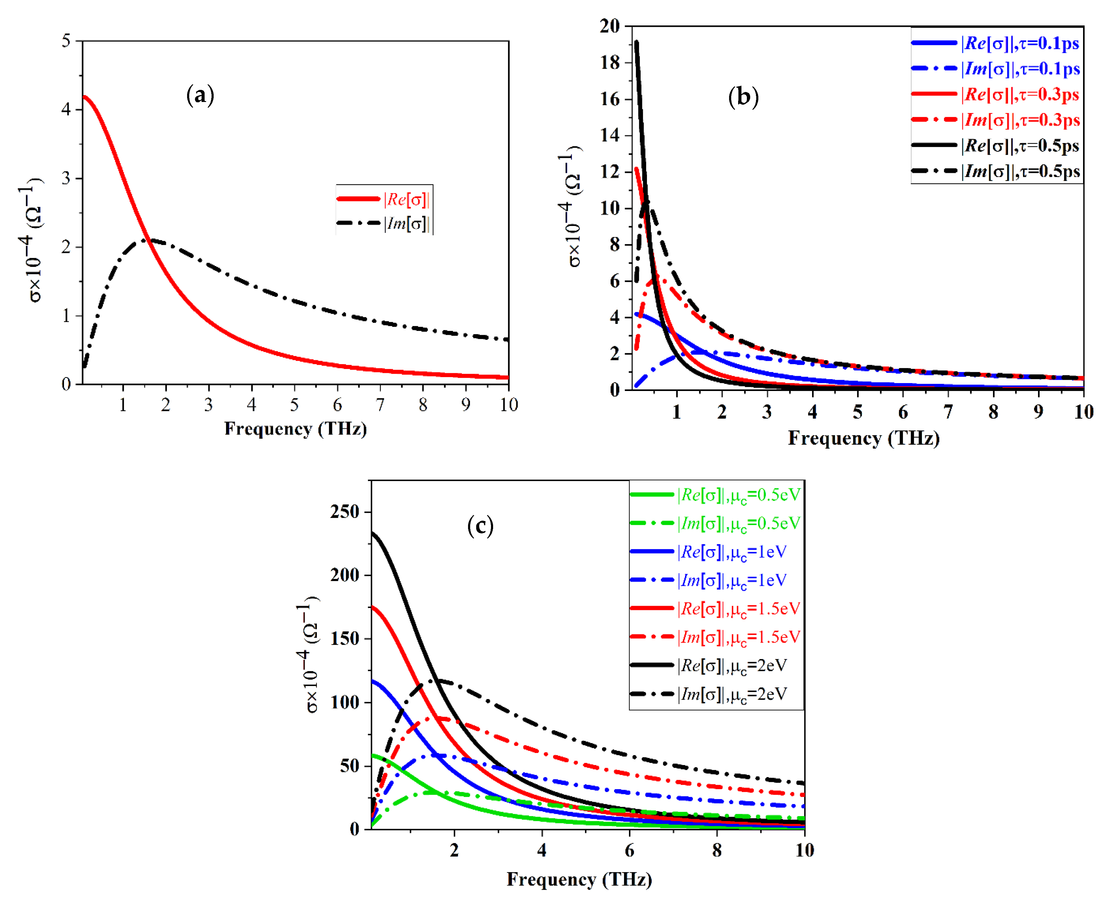
2.1. Graphene’s Conductivity and Dispersion Relation

Graphene, as a carbon-based material, has been prepared with different techniques. A single layer of graphene was extracted from the bulk graphite crystal structure using a mechanical exfoliation approach. Chemical vapor deposition (CVD), thermal exfoliation, and carbon segregation [27] are other preparation methods for the graphene layers. At the THz frequency band, this exceptional material exhibits excellent mobility, transparency, flexibility, and environmental stability. As a result, it is the best choice that can be used in antenna applications. In comparison to other nano-plasmonic materials such as gold and silver, graphene is an excellent contender for promoting the propagation of SPP waves. The dispersion relation of Transverse Magnetic (TM) of SPP depends on the conductivity of graphene given by [28].
i σ s ω ε 0 = ε r 1 + ε r 2 coth ( K e f f t o ) K e f f
where ε r 1 and ε r 2 are the relative permittivity of air over the graphene layer and the dielectric constant of the substrate materials, respectively. Keff, is the wavenumber of the SPP wave which can be expressed by:
K e f f = K 0 ( η e f f )
where η e f f is the effective refractive index of SPP and K 0 is the free space wavenumber K 0 = 2 π λ . According to Kubo’s formula [29,30]. The graphene conductivity is the sum of both intraband and interband conductivity, and can be described as:
σ s = σ i n t e r + σ i n t r a  
σ s ( ω , μ c , τ , T ) = j e 2 ( ω j τ 1 ) π 2 × [ 1 ( ω j τ 1 ) 2 0 ( f d ( ε ) ε f d ( ε ) ε ) d ε 0 f d ( ε ) f d ( ε ) ( ω j τ 1 ) 2 4 ( ε ) 2 d ε ]
f d ( ε ) = 1 [ e ( ε μ c ) / K B T + 1 ]
where T is the temperature, K B is the Boltzmann constant, is the reduced Plank’s constant, μ c is the chemical potential, e is the charge of electron τ is the relaxation time and f d ( ε ) is the Fermi-Dirac distribution. The first term in the preceding equation denotes graphene’s intraband conductivity, whereas the second term denotes graphene’s interband conductivity. Intraband conductivity dominates in the MW and THz bands, whereas interband conductivity dominates in the near-infrared and visible spectrums [31]. Graphene’s intraband and interband conductivities can be expressed as:
σ i n t r a ( ω , μ c , τ , T ) = j e 2 K B T π 2 ( ω j τ 1 ) [ μ c K B T + 2 ln ( e μ c / K B T + 1 ) ]
σ i n t e r ( ω , μ c , τ , T ) = j e 2 4 π l n [ 2 | μ c | ( ω j τ 1 ) 2 | μ c | + ( ω j τ 1 ) ]

2.2. Graphene Modeling

The graphene layer is simulated and optimized using CST Microwave Studio, which is based on the Finite Element Method (FEM). This program has two built-in graphene models, namely “graphene” and “graphene-Eps”. The first model uses a single layer of graphene with a thickness of 0.345 nm, whereas the second uses a multilayer of graphene sheets with varying thicknesses. In this paper, we proposed an application of a single layer of graphene sheet of 0.34 nm thickness for our presented graphene plasmonic nanoantenna. Figure 1a shows the graphical representation for the surface conductivity of the graphene layer at zero value of chemical potential and the relaxation time is 0.1 p sec at room temperature which is identical to the one presented by Llatser et al. [32].
The real and imaginary parts of our simulated graphene are presented in Figure 1b,c for various relaxation time (τ) and chemical potential (µc) values, respectively, using the MATLAB program. This figure demonstrates that the overall conductivity of a graphene slab is strongly reliant on the chemical potential and the relaxation time. Chemical potential is proportional to carrier density, which can be varied via an external gate voltage or chemical doping:
n = 2 π 2 v f 2 0 [ f d ( μ c ) f d ( + μ c ) ] d
The relationship between the chemical potential and gate voltage is explained by [33]. Tunability is required for the wideband operation of the proposed antennas which can prevent path loss and enhance data rates in THz communication systems. Tunable antennas have been considered the best tools for manipulating the interaction of light with electrons present in materials. The fundamental capabilities of graphene antennas are vastly utilized in a broad scope of practices, including high-speed communication with high data rate, terahertz detection energy harvesting, and optical light emission.
V g = [ e μ c 2 h π 2 v f 2 ε 0 ε r ]
where h is the substrate thickness and ε r is the relative permittivity of the substrate material. The conductivity of graphene can be changed with the relaxation time (τ) as follows [34].
τ μ g n π e v f
where μ g is the electron mobility of graphene and v f is the Fermi velocity. The relaxation time increases with the chemical potential values. Long relaxation time supports the propagation of the SPP wave.

3. Antenna Design

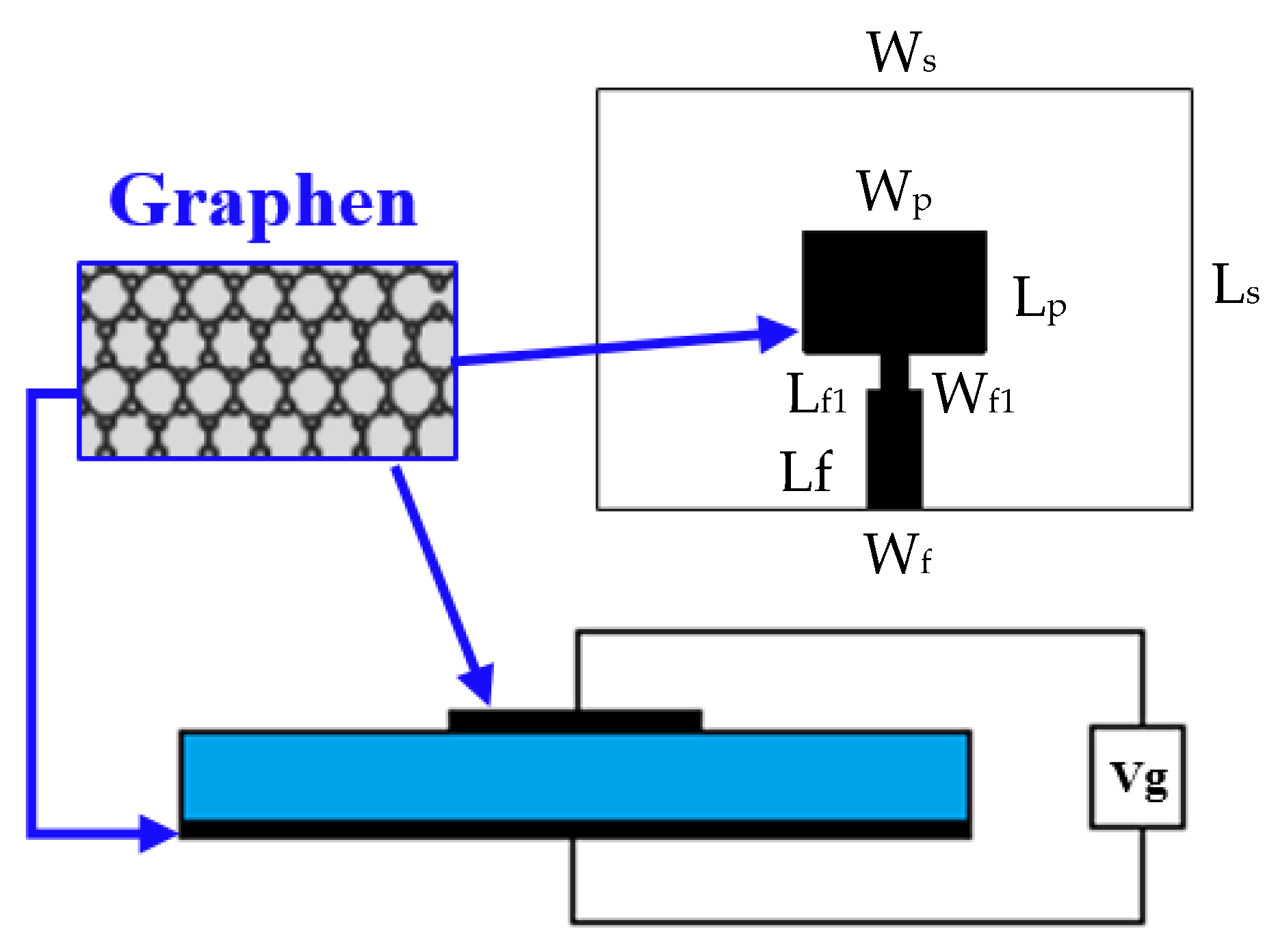
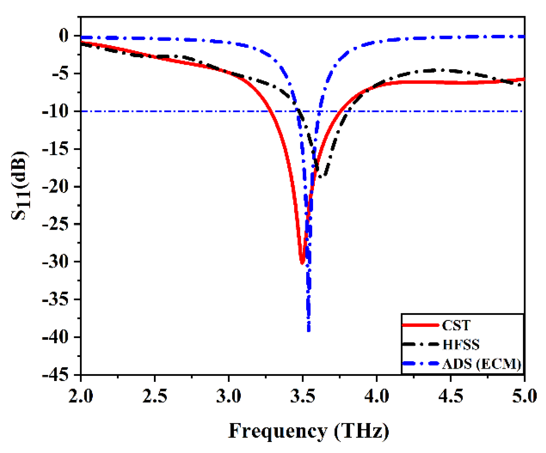
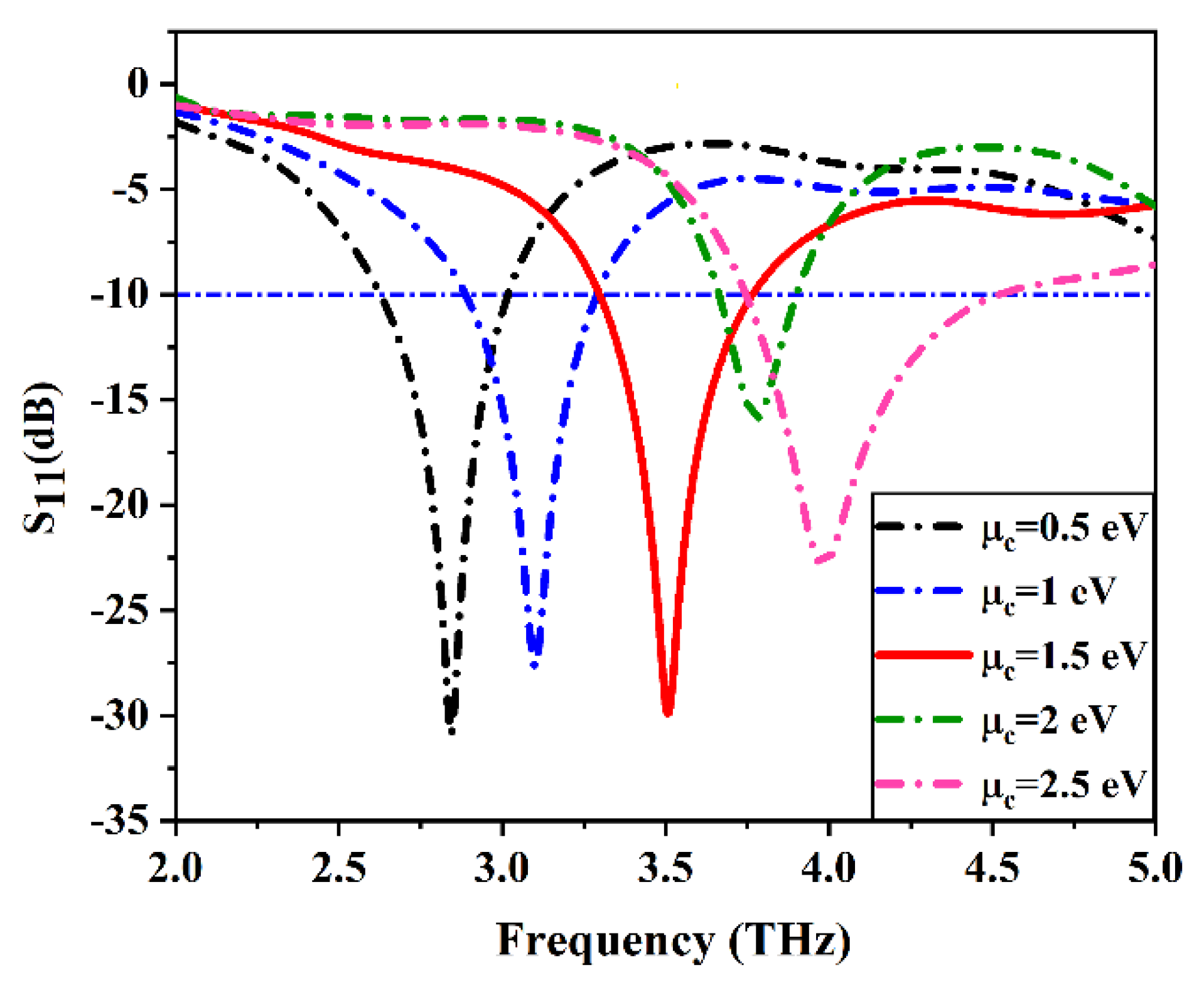
3.1. Single Element Patch Antenna

Initially, a conventional microstrip patch antenna with a graphene plasmonic layer is engraved on the top side of Teflon with a relative permittivity of 2.1, and a thickness of 10 µm. The proposed antenna is designed to resonate at 3.5 THz. The dimensions of the patch are recognized by the usage of the characteristic mode analysis (CMA) using the integral equation solver in the CST microwave studio. The optimum width and length of the patch are 32 µm and 25 µm, respectively. The single element of the patch antenna is matched to a transmission line of 50 Ω characteristic impedance using a quarter-wavelength impedance transformation. The model significance and the characteristic angel curves are shown in Figure 2a,b. Mode 1 is the resonance mode (desired mode) at a frequency of 3.5 THz in which the characteristic angle is 180° and the model significance in this frequency is the highest value (closely to unity). The validation process of the CST result can be achieved by the usage of HFSS and the equivalent circuit model using ADS software. The values of the electrical RLC components are calculated, and the electric circuit model of the antenna is developed using the circuit theory approach [35].
The desired current distribution specifies the optimum position for the excitation process so, the proposed structure of the single-element antenna is shown in Figure 3. The calculated value of the circuit parameters is listed in Table 1. Figure 4 shows the circuit model connection diagram of the proposed antenna. The results obtained from the HFSS and ADS circuit theory approach are in good agreement with those obtained using CST software. The |S11| curve of the graphene plasmonic antenna is illustrated in Figure 5. There is a small deviation in the |S11| curves, which may be due to the different numerical approaches used in different software. The 3D radiation pattern of the proposed graphene plasmonic antenna is depicted in Figure 6. Figure 7 shows the graphene’s frequency-reconfigurable behavior of the graphene plasmonic antenna when the chemical potential applied varied between 0.5 and 2.5 eV. This figure reveals that the plasmonic resonance frequency of the proposed antenna increases via the chemical potential and can be dynamically controlled in a wide frequency range from 2.75 to 4 THz. So, this design has dynamic reconfigurability by applying an external electric field.

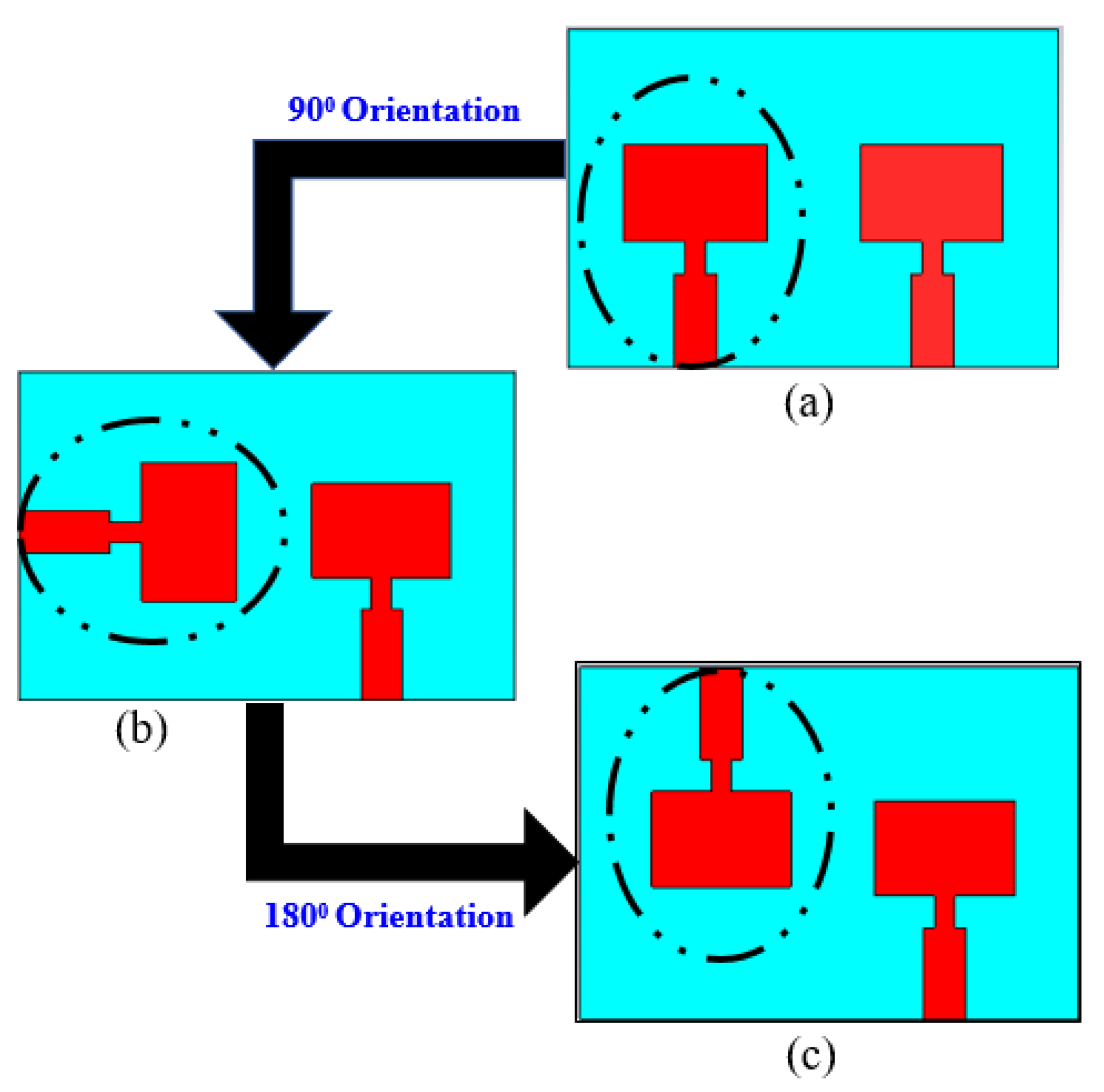
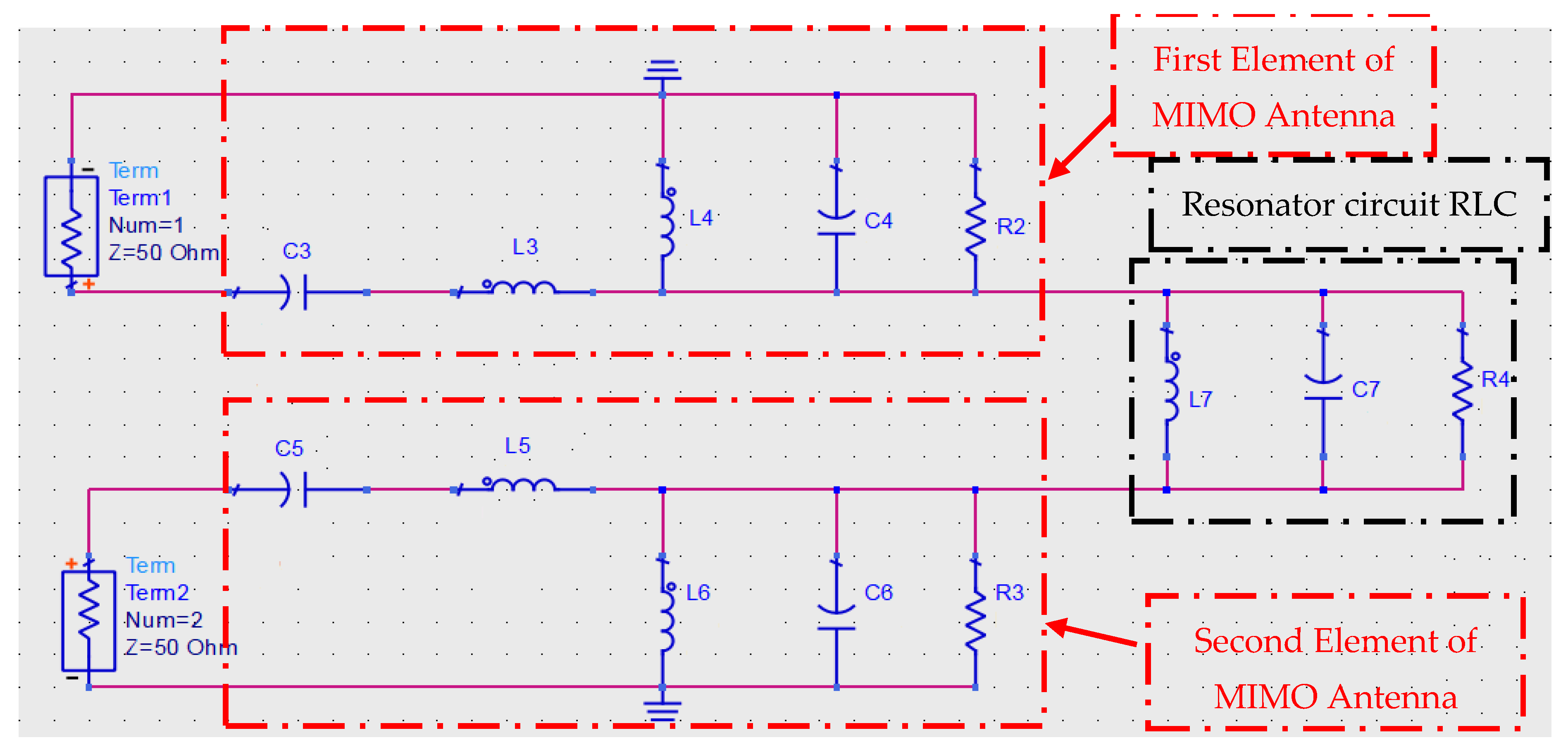
3.2. Two Elements Graphene Plasmonic MIMO Antenna Configurations

The MIMO system’s advantage is that it provides data rate augmentation even in the presence of signal fading, multipath fading, and interference. The MIMO system was designed to meet the requirements of acceptable MIMO parameters because of the need to transmit more data over greater distances. Mutual coupling between elements in a MIMO array could alter the performance of a single-element antenna. The distance between the MIMO units regulates this mutual coupling, which is formed via electromagnetic interaction between them. The optimum separation distance between adjacent MIMO elements is the system’s most important goal. An antenna with a large distance between elements ensures non-correlation but increases the overall antenna size, whereas a small distance will increase the mutual coupling between the elements. So, mutual coupling is an important parameter that should be studied that faces the MIMO antenna systems. The two-element graphene plasmonic microstrip MIMO patch antennas are illustrated in the following part. In order to create the optimal MIMO antenna configuration, it is necessary to first determine the orientation of the optimal elements to achieve the desired high level of isolation. Figure 8 demonstrates the proposed three configurations that are used in the antenna design. The first configuration (Ant. A) is shown in Figure 8a the two elements have a 0° orientation side by side with the first element. The second configuration (Ant. B) is shown in Figure 8b where the two elements are orthogonally oriented with a 90° between them. In the last configuration (Ant. C), the two elements have a 180° orientation as shown in Figure 8c. The simulated reflection coefficients |S11| and transmission coefficients |S21| versus frequency of the three MIMO configurations are investigated in Figure 9. The transmission coefficients |S21| are an important parameter while designing the MIMO system. It is the measurable parameter of the mutual coupling between the MIMO elements.
These are three possible orientations that can be used using two elements MIMO antenna. Figure 9 illustrates the |S11| parameters of the three MIMO configurations that are designed to resonate at 3.5 THz. The |S21| curves reveal that Ant. C has the lowest mutual coupling of −25.6 dB within the entire interested frequency band rather than the other configurations of Ant. B that has a −22.4 dB in addition, the Ant. A has a mutual coupling of −18 dB The three graphene patch MIMO configurations are printed on Teflon substrate with a relative permittivity ( ε r ) of 2.1 and a thickness of 10 µm. The CMA is used to describe the behavior of the graphene plasmonic MIMO antenna configurations with the help of model significant (Ms), and the model current distribution for the three configurations of Ant. A, Ant. B and Ant. C.

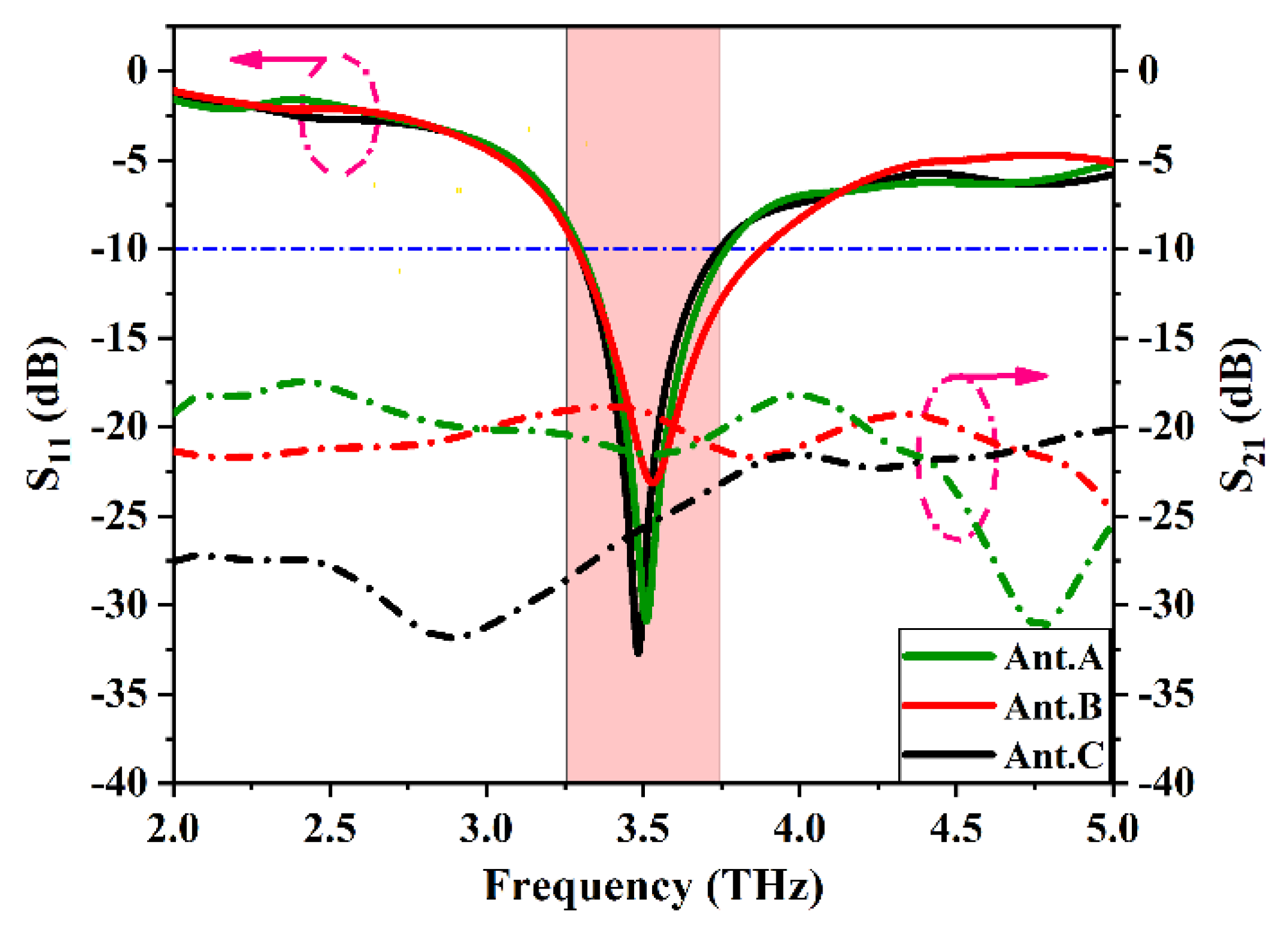
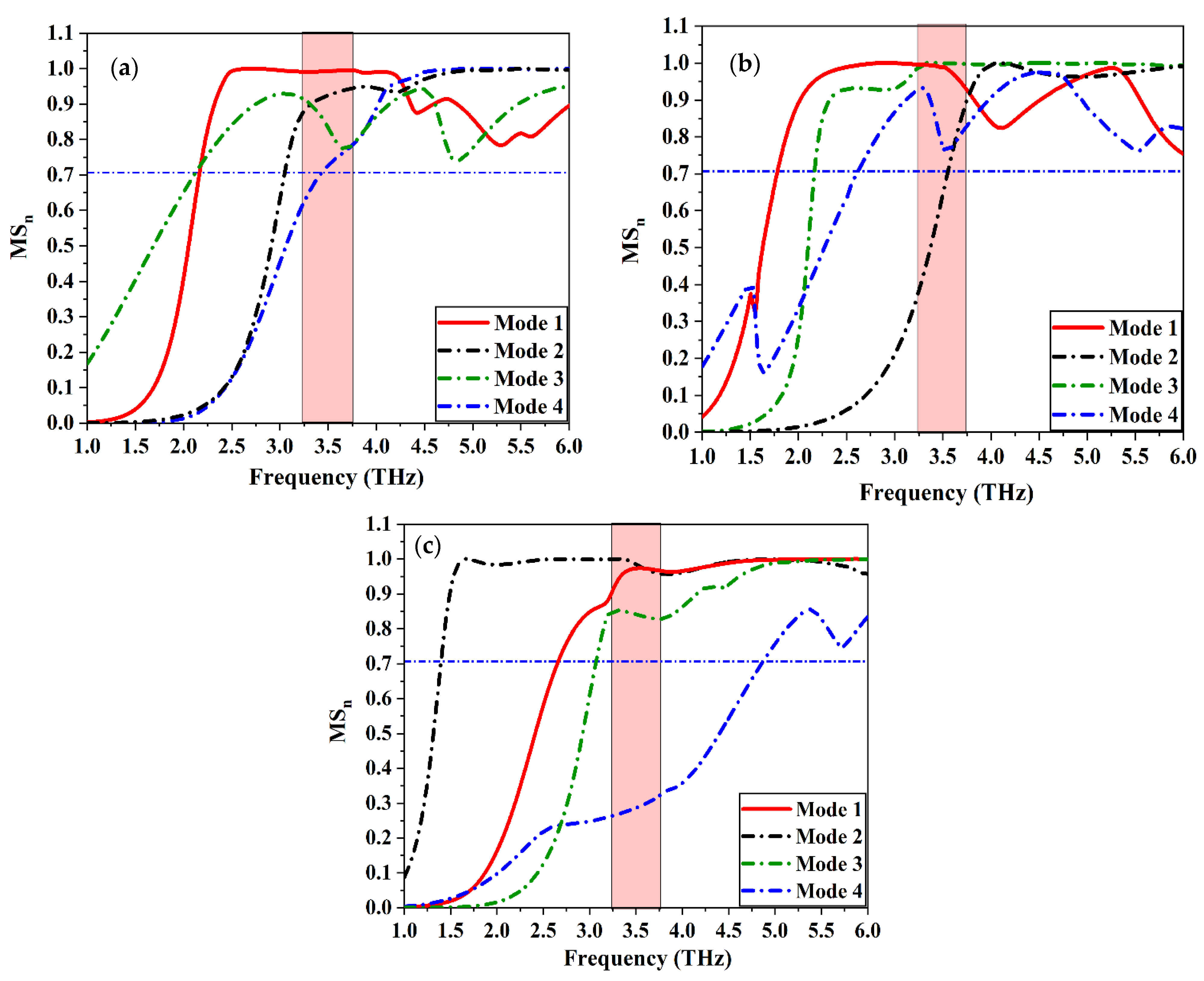
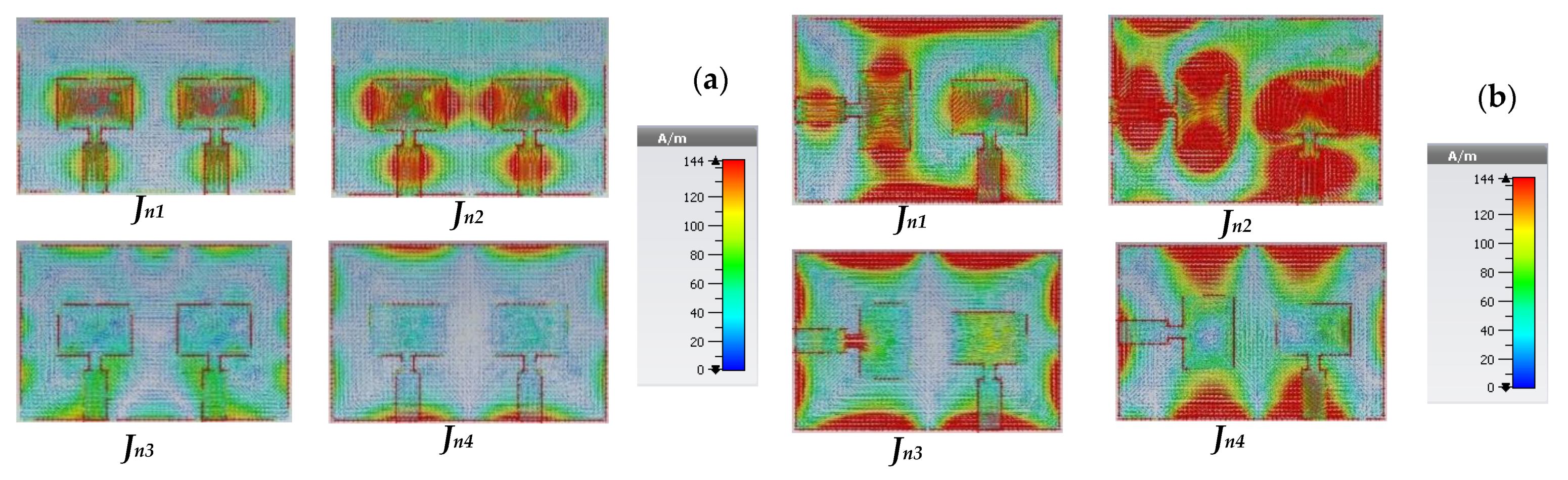
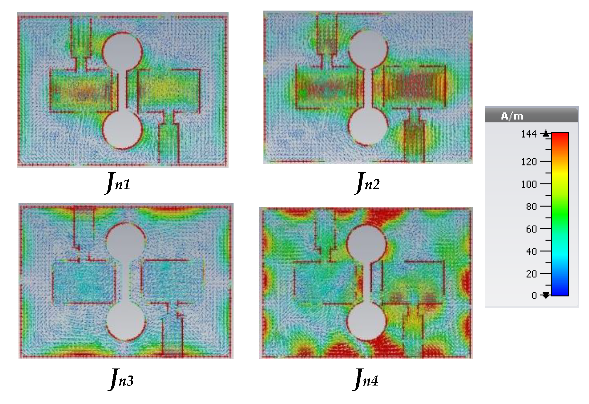
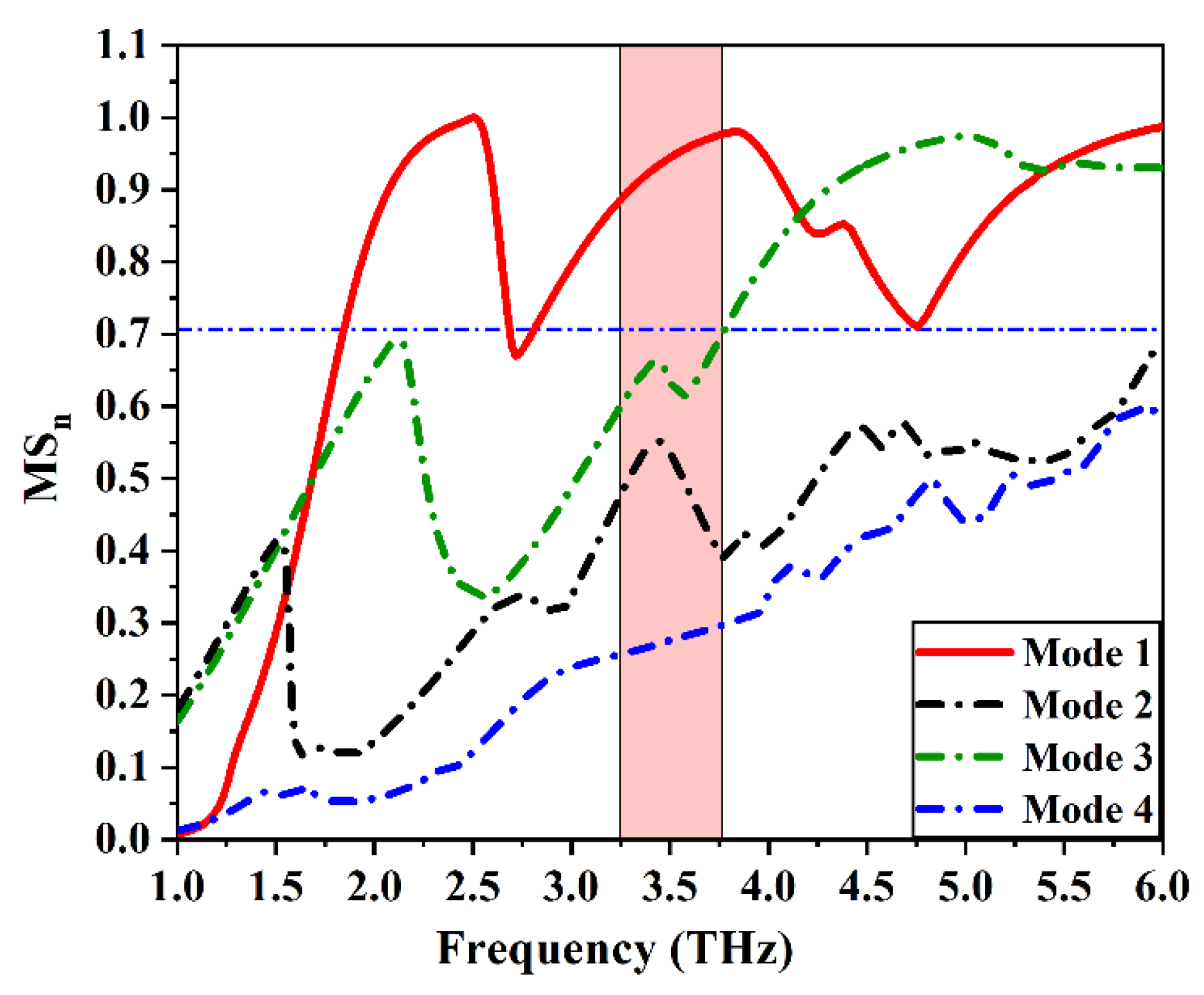
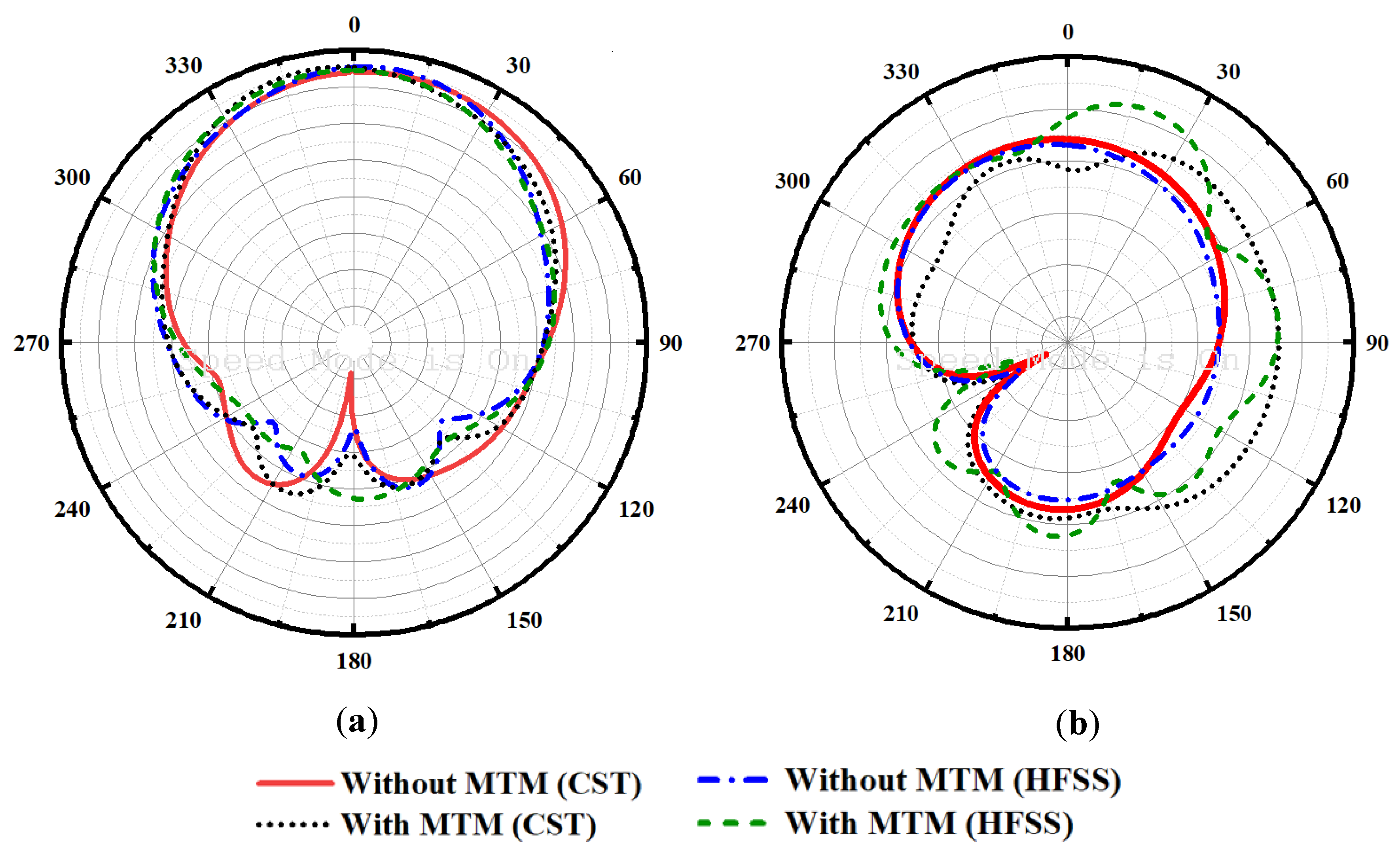
3.3. Analysis of the Graphene Plasmonic MIMO Configurations

The evaluation of the two-element graphene plasmonic MIMO antenna structure is carried out and optimized using CMA for three different configurations. Firstly, in Ant. A structure, the model significance, and the model current distribution curves at the resonance frequency of 3.5 THz are investigated in Figure 10a and Figure 11a, respectively. The model significance curve indicates the first four modes of operation through the entire band. It can be seen that the four modes play a significant role in the desired bandwidth ( M s 0.707 ), but modes 1 and 2 give a high contribution in the desired bandwidth rather than modes 3 and 4. Moreover, modes 1 and 2, have the highest values (close to unity). So, it is expected that one of these modes is responsible for the antenna resonation at 3.5 THz and the other one is responsible for coupling between the two-elements’ graphene plasmonic MIMO antenna. The model current distribution makes the divergence between the first two modes. From the current distribution depicted in Figure 11a; mode (Jn1) is the dominant mode that is responsible for the antenna resonation and mode (Jn2) causes the coupling between the two-radiating elements of the MIMO antenna because of the high current density between the elements which, in turn, affects the overall antenna performance negatively. Therefore, it is imperative that the characteristics of this mode need to be tuned again with a certain approach. In addition, mode (Jn3) and mode (Jn4) have no impact on the coupling between the MIMO elements. Secondly, in Ant. B, the model significant curve shown in Figure 10b illustrates the first four modes. It can be seen that all modes have the opportunity to contribute to the radiating bandwidth ( M s 0.707 ) with different levels of acceptance such as modes 1 and 3, which have the highest values of M s , while modes 2 and 4, have the lowest one. So, the model significant property is not sufficient to specify all the modes and clarify which of them is responsible for the coupling, non-coupling, and resonance effect. The model current distribution in Figure 11b is a good candidate that is used to illustrate this point. This figure reveals that modes (Jn3) and, (Jn4), have a current null between the antenna elements, and mode (Jn1) is the resonance one while mode (Jn2) is the coupling mode that needs to be characterized and tuned again to reduce the mutual coupling between the graphene plasmonic MIMO antenna elements. Finally, in Ant. C configuration, the model significant curve depicted in Figure 10c demonstrates the first four modes that participate in the desired bandwidth ( M s 0.707 ). It is interesting to note that, modes 1,2, and 3 only contribute to the desired bandwidth of the antenna as they have the highest value of M s . However, mode 4 can be neglected because of its low value of M s within interested bandwidth. This result can be assured by introducing the model current distribution in Figure 11c. From this curve, we can overlook mode (Jn3) and (Jn4) as the current density concentration is very weak between the patches. So, mode (Jn1) is the resonance mode, and mode (Jn2) is the coupling one. The model significance and model current distribution curves of the proposed three configurations of the MIMO antenna reveal that the configuration of the designed antenna is responsible for the degree of the coupling between the two elements. The model current distribution indicates that the best configuration is Ant. C which gives a low coupling between the patches and low current density concentration in comparison with Ant. A and Ant. B.

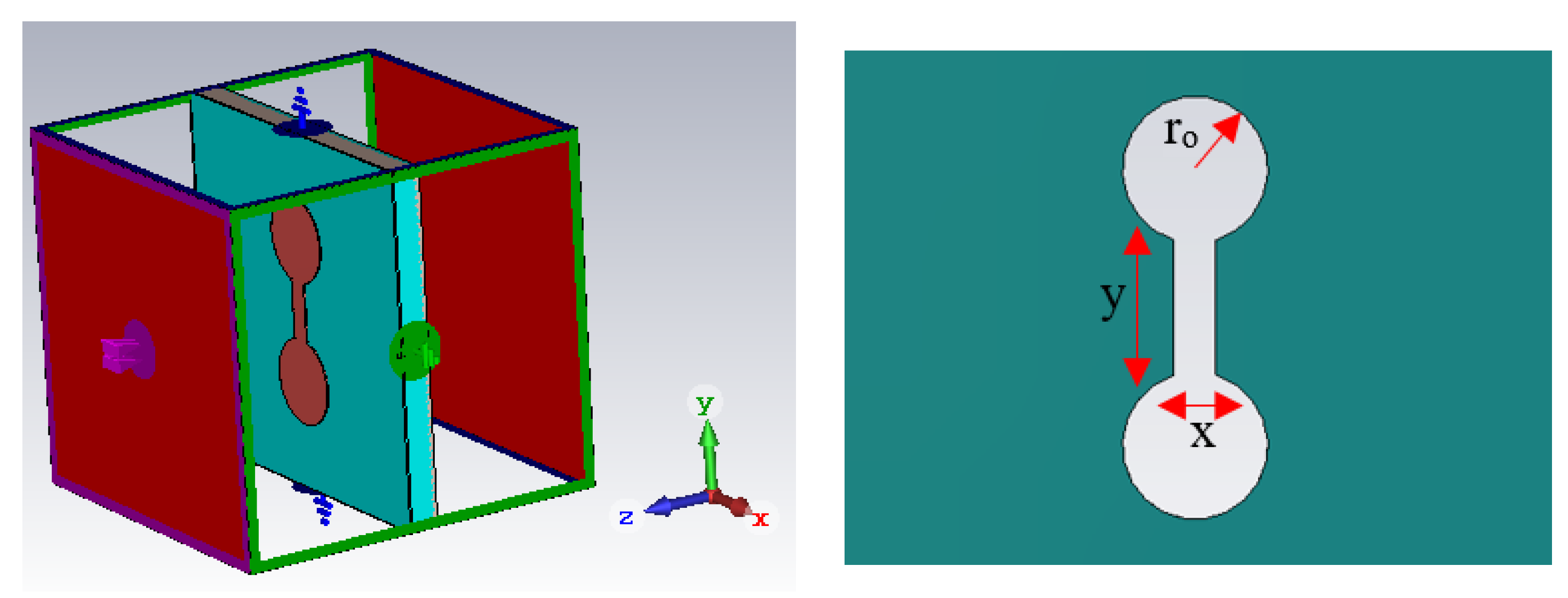
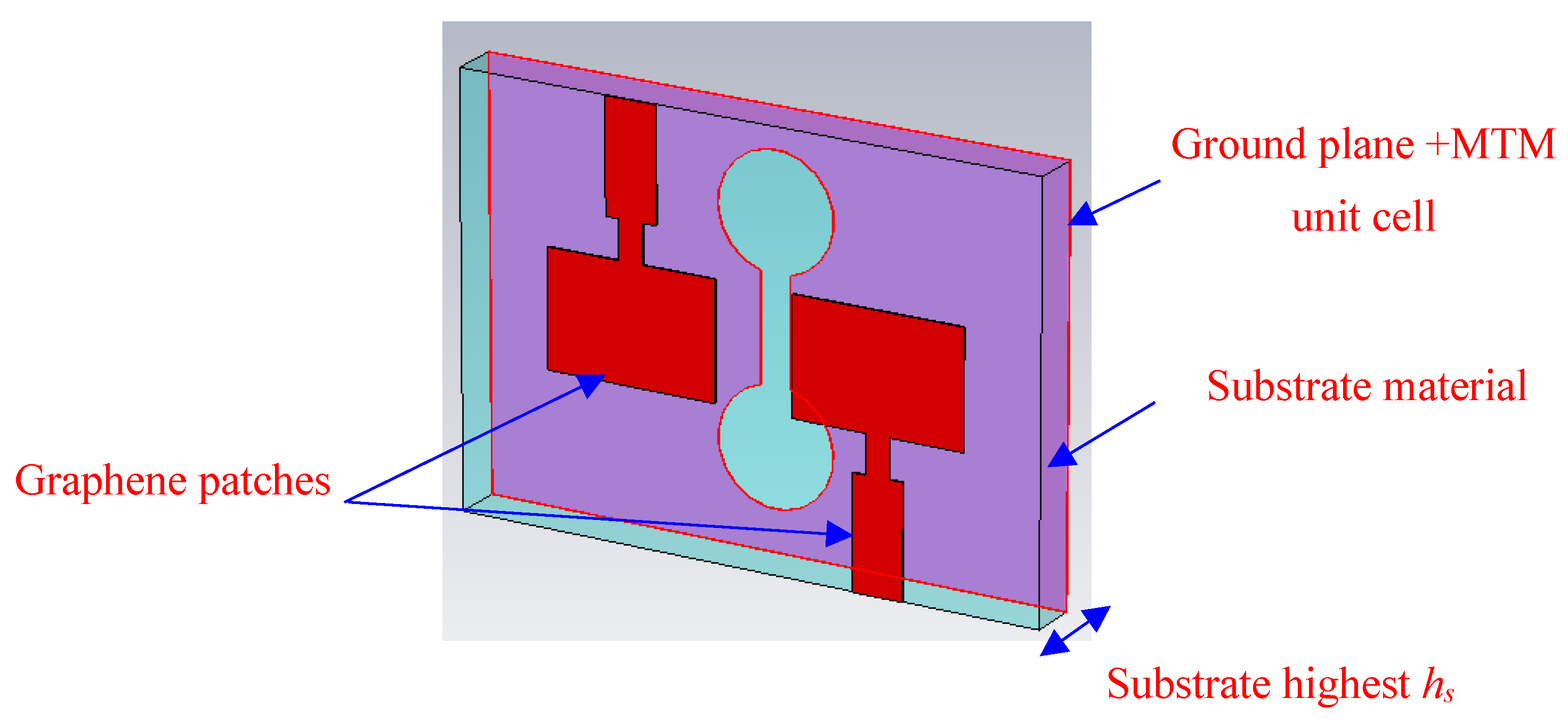
3.4. De-Coupling Structure of Dumbbell Shape MTM Unit Cell

As the distance between the elements of the MIMO antenna is responsible for the mutual coupling issue, the performance of the antenna seriously deteriorates as this distance decreases. The three configurations of the MIMO antenna introduced above suffer from mutual coupling problems, so, a de-coupling structure is needed to overcome this problem. A complimentary new shape of Dumbbell-structure MTM unit cell is etching in the ground plane with a strong band rejection characteristic (Band-stop Filter) illustrated in Figure 12 and its dimensions listed in Table 1. The S-parameter curve depicted in Figure 13 illustrates that the Dumbbell-structure MTM unit cell has a high band-stop characteristic |S21|. The permittivity and permeability of the unit cell in Figure 14a,b reveal that this structure is an MTM unit cell with a negative value if ( ε r and μ r ) in the desired bandwidth. The MTM unit cell of the Dumbbell-structure that is etched in the ground plane will reduce the mutual coupling between the two elements of the graphene MIMO configurations due to its band rejection characteristic at the desired frequency band. As mentioned before, in the proposed three configurations there is only one mode responsible for the coupling between the two elements (mode 2) in all configurations. So, this mode should be returned to improve the isolation. The MTM unit cell is designed to produce a current flow distribution in the opposite direction of the coupling mode current (mode 2). The characteristic mode theory (CMA) has a vital role in illustrating the behavior of the graphene MIMO systems with and without introducing the Dumbbell-structure unit cell by the usage of model significant and model current distribution. The Ant. C is the best choice to invoke the MTM unit cell on its ground plane as it has a good characteristic rather than the other configurations.
In Ant. C configuration, with the presence of an MTM unit cell as depicted in Figure 15, the model current distribution of the first four modes is shown in Figure 16. It can be seen that the mutual coupling is reduced and the path of the current through the MTM design is orthogonal to the path of the current that occurred due to the coupling mode (mode 2). So, the net interference between the two patches is remarkably reduced. This result can be assured from the model significance curve illustrated in Figure 17, we can note that the first four modes of operations and only mode 1 affects the desired bandwidth ( M s 0.707 ) . Mode 2, which is responsible for the coupling is moved away from the bandwidth in the condition that the resonance mode 1 does not affect and stays the same. Moreover, modes 3 and 4 do not affect the desired bandwidth which can be seen from the model current distribution and model significant curves. At last, from the study of the CMA analysis in the three proposed configurations of graphene MIMO antenna, introducing the Dumbbell-structure MTM unit cell in the ground plane has a good impact on the MIMO antenna parameters, especially in the interference problem between the patches that enhance the overall performance of the antenna. Ant. C, in the presence of an MTM unit cell, is the preferable configuration of the two-element graphene plasmonic MIMO structure, which gives high isolation between the patches as shown in Figure 18, which presents the |S11| and |S21| of the proposed antenna with and without the presence of the MTM unit cell.
The S–Parameters and the ADS for the equivalent circuit models of the proposed design are listed in Figure 19 and Figure 20 respectively. The isolation coefficient |S21| has been reduced from −25 dB to −55 dB because of the introduction of the Dumbbell-structure MTM unit cell in the ground. The ADS software is used to validate the results by using the equivalent circuit model (ECM) analysis. The ECM consists of a two-input port with 50 Ω input impedance and is separated by the resonator circuit that represents the Dumbbell-structure MTM unit cell. The calculated values of the circuit elements are listed in Table 1. The S–Parameters of the ECM analysis is compared with the CST microwave studio. It can be seen that the ADS results are in good agreement and coincide with the CST result with a little change due to the values of the RLC components.

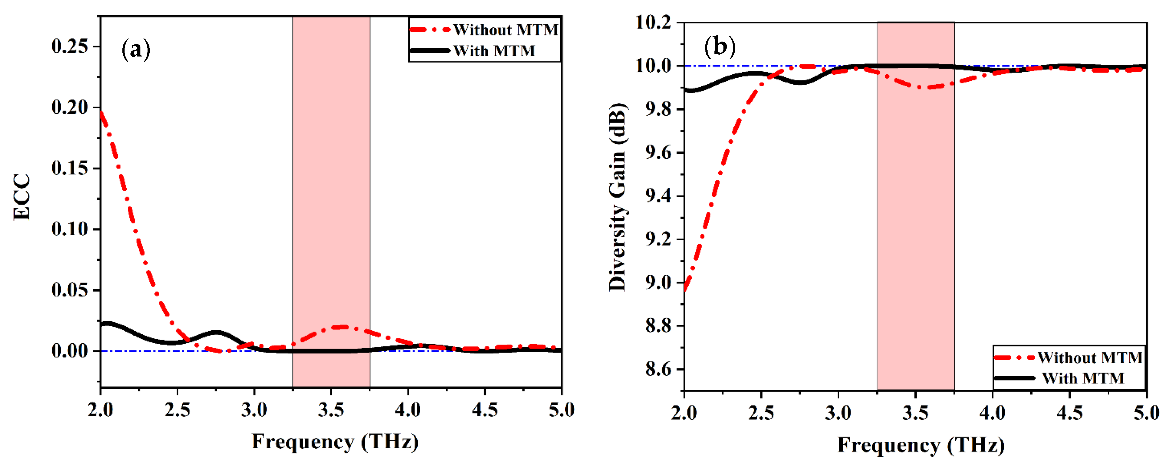
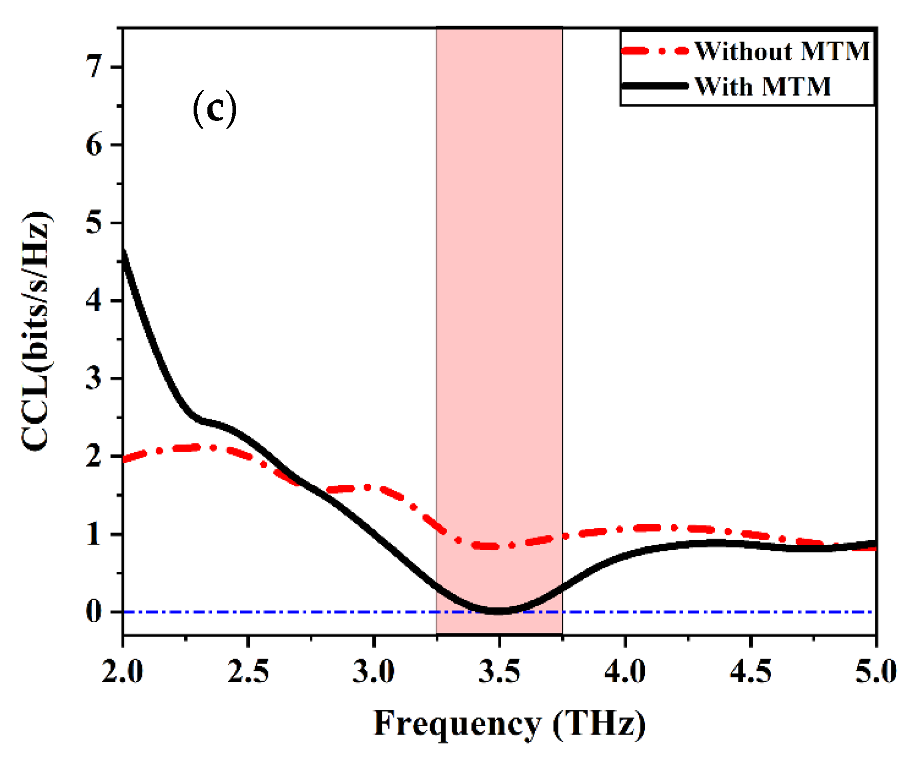
3.5. Analysis of MIMO Antenna Parameters

In this section, we discuss the most important parameters of the MIMO antenna structure. These parameters are very crucial in the MIMO systems. As the demand for a higher data rate for long-distance transmission is one of the major motivations behind the MIMO configuration to ensure the compatibility of the graphene plasmonic MIMO antenna in the THz frequency band. The envelope correlation coefficient (ECC), diversity gain (DG), and channel capacity loss (CCL) are evaluated and discussed [36,37]. The ECC is defined as the correlation between the patches in the chosen MIMO configuration. The lower amount of ECC between the MIMO elements means higher MIMO performance. There are two methods to extract the ECC parameters, the first one is by extracting from the S–Parameters as in [38].
E C C = ρ i j = | S 11 * S 12 + S 21 * S 22 | 2 ( 1 ( | S 11 | 2 + | S 21 | 2 ) ) ( 1 ( | S 22 | 2 + | S 12 | 2 ) )
where S 11 * and S 21 * represent the conjugate of S 11 and S 21 , respectively. The second one is by extracting from the 3D radiation pattern as illustrated in [25].
E C C = ρ i j = | 4 π [ F i ( θ , φ ) F j ( θ , φ ) ] d Ω | 2 4 π | F i ( θ , φ ) | 2 d Ω   4 π | F j ( θ , φ ) | 2 d Ω
where F n ( θ , φ ) is the 3D field radiation pattern of the elements associated with the nth port, denotes the Hermitian product operator and Ω represents the solid angle. The evaluation of the ECC using a far-field radiation pattern is a complex method, so the S–Parameters method is very convenient to calculate the ECC between the two antenna elements as it is faster and easy to be used as it depends only on the port parameters of the antenna system. The agreeable limit of the ECC is lower than 0.5. The proposed graphene plasmonic MIMO antenna is simulated and ECC is calculated and displayed in Figure 21a. This figure reveals the comparisons between the MIMO elements with and without introducing the complementary Dumbbell-structure MTM unit cell in the ground plane. The ECC without MTM has a value of 0.0189, while the ECC with MTM is reduced to 0.000168 through the entire bandwidth of operation. The lower value of ECC indicates a lower correlation between antenna elements. This value guarantees good MIMO performance of the proposed antenna. Another way to describe and evaluate the performance of the MIMO antenna structure is the diversity gain (DG), which describes the losses that occur in the transmitted power. The formula given in [39] is used to calculate the DG value:
D G = 10 1 ( E C C ) 2
It can be seen that the DG depends on the value of ECC, moreover, equation (18) states that the small value of ECC produces a higher value of DG and makes the MIMO antenna suitable for diverse applications. Figure 21b depicts the DG value of the proposed MIMO structure in the presence and absence of the MTM structure it has a value of 9.999 and 9.904, respectively.
Channel capacity loss (CCL) is one of the most significant MIMO parameters that describe the potential loss of channel capacity due to the correlation between the MIMO antenna elements, in other words, CCL defines the maximum limit of information transmission rate without significant loss. It should be less than 0.5 bits/s/Hz for a well-designed MIMO configuration. The CCL is indicated in (19) as reported in [39].
C C L = log 2 [ det ( Φ k ) ] ,
Φ k = [ ρ 11 ρ 12 ρ 21 ρ 22 ]
ρ i i = ( 1 ( | S i i | 2 + | S i j | 2 ) ) ,         a n d
ρ i j = ( S i i * S i j + S i j * S j j ) ,
where Φ k indicates the correlation matrix at the receiving antenna. Figure 21c depicts the simulated CCL of the proposed MIMO antenna. It recorded the specified limit for the proposed MIMO configuration. A comparison between the CCL curves with and without introducing the MTM unit cell. So, it has a value of 0.006 and 0.840, respectively. It can be confirmed that the proposed design of graphene plasmonic MIMO configuration delivers a higher transmission data rate in any scattering environment. Figure 22 illustrates the representation of the far-field radiation pattern component of the E and H plane at 3.5 THz. The E and H plane radiation patterns are represented in terms their components. The proposed graphene plasmonic MIMO antenna radiation patterns are illustrated in the presence and the absence of the MTM unit cell. The proposed MIMO configuration exhibits a little change in the E and H planes as shown in Figure 22. At last, the E and H patterns indicate that no significant difference between the main lobe pattern with and without the Dumbbell-structure MTM unit cell.

3.6. Performance Analysis with State-of-the-Art of Printed THz Antennas

In this part, comparisons between proposed optimized Ant. C design with previously reported antennas has been performed for the terahertz frequency band. The comparison is conducted based on performance parameters such as gain, size of the antenna elements, and resonance frequency. Moreover, the MIMO parameters such as ECC, DG, and CCL are tabulated in Table 2. Based on the presented data, we can conclude that the proposed graphene plasmonic MIMO antenna has the best isolation and ECC. Although the proposed design presents a high gain with all compared references, the design in [40] has a higher gain, but gives low isolation and CCL. Finally, the proposed antenna demonstrates a superior MIMO performance to that of the other listed designs in Table 2. So, it is a good candidate to be used in 6G for mobile generation and medical applications. It has a suitable compact size to easily integrate with on-chip integrated circuits.

4. Conclusions

In this paper, a high-performance graphene plasmonic two-port MIMO antenna has been introduced to be used in terahertz wireless communication applications. In the theory of characteristic mode analysis (CMA) with the help of a complementary Dumbbell-structure MTM unit cell, the mutual coupling between the antenna elements has been significantly reduced. The MTM structure acts as a band stop filter in the desired bandwidth. It is etched in the ground plane so as to reduce the mutual coupling from −25 dB to −55 dB in the presence of the MTM unit cell. The CMA has been used to study the behavior of the antenna modes of operations and clarify the mode responsible for the coupling between the elements and detect the optimum position of this mode which can be illuminated by the MTM structure without any distortion in the main antenna resonance mode (dominant mode). Furthermore, the MIMO antenna parameters such as ECC, DG coefficients, and CCL are investigated and presented to confirm the suitability of the proposed graphene MIMO antenna for different THz applications. The proposed MIMO antenna resonates at 3.5 THz with a return loss of −35 dB and exhibits a wide impedance characteristic bandwidth covering 3.2 to 3.8 THz frequency spectrum in the THz regime (BW = 600 GHz). The designed MIMO antenna maintains maximum isolation of −55 dB at the resonance frequency of 3.5 THz. The good MIMO performance is ensured by achieving the MIMO performance parameters (ECC = 0.000168, DG = 9.999, and CCL = 0.006) within acceptable limits. The proposed MIMO antenna design in the future can be used as a massive MIMO and used the reconfigurable intelligent surfaces to be suitable for the 6G communication technology The proposed MIMO antenna is suitable for high-speed short-distance indoor communication applications such as video-rate imaging, biomedical imaging, sensing, and security scanning in the terahertz frequency band.

Author Contributions

S.A.K. raised the idea, wrote the manuscript, and perform the numerical simulations, E.K.I.H. and N.O.P., revised the manuscript and perform the theoretical analysis, N.O.P. and M.B.S., discussed the numerical results in the main manuscript; S.A.K. and E.K.I.H. contribute to the simulation results and the validation, improved the revised version. All authors have read and agreed to the published version of the manuscript.

Funding

This research received no external funding.

Institutional Review Board Statement

Not applicable.

Informed Consent Statement

Not applicable.

Data Availability Statement

All the data have been included in the study.

Conflicts of Interest

The authors declare no conflict of interest.

References

  1. Giordani, M.; Polese, M.; Mezzavilla, M.; Rangan, S.; Zorzi, M. Toward 6G Networks: Use Cases and Technologies. IEEE Commun. Mag. 2020, 58, 55–61. [Google Scholar] [CrossRef]
  2. Alsabah, M.; Naser, M.A.; Mahmmod, B.M.; Abdulhussain, S.H.; Eissa, M.R.; Al-Baidhani, A.; Noordin, N.K.; Sait, S.M.; Al-Utaibi, K.A.; Hashim, F. 6G Wireless Communications Networks: A Comprehensive Survey. IEEE Access 2021, 9, 148191–148243. [Google Scholar] [CrossRef]
  3. Chowdhury, M.Z.; Shahjalal, M.; Ahmed, S.; Jang, Y.M. 6G Wireless Communication Systems: Applications, Requirements, Technologies, Challenges, and Research Directions. IEEE Open J. Commun. Soc. 2020, 1, 957–975. [Google Scholar] [CrossRef]
  4. Akyildiz, I.F.; Jornet, J.M.; Han, C.J.P.C. Terahertz Band: Next Frontier for Wireless Communications. Phys. Commun. 2014, 12, 16–32. [Google Scholar] [CrossRef]
  5. Tekbıyık, K.; Ekti, A.R.; Kurt, G.K.; Görçin, A.J.P.C. Terahertz Band Communication Systems: Challenges, Novelties and Standardization Efforts. Phys. Commun. 2019, 35, 100700. [Google Scholar] [CrossRef]
  6. Hosseininejad, S.E.; Alarcon, E.; Komjani, N.; Abadal, S.; Lemme, M.C.; Bolívar, P.H.; Cabellos-Aparicio, A. Study of hybrid and pure plasmonic terahertz antennas based on graphene guided-wave structures. Nano Commun. Netw. 2017, 12, 34–42. [Google Scholar] [CrossRef] [Green Version]
  7. Koenig, S.; Lopez-Diaz, D.; Antes, J.; Boes, F.; Henneberger, R.; Leuther, A.; Tessmann, A.; Schmogrow, R.; Hillerkuss, D.; Palmer, R.; et al. Wireless sub-THz communication system with high data rate enabled by RF photonics and active MMIC technology. In Proceedings of the IEEE Photonics Conference, San Diego, CA, USA, 12–16 October 2014; IEEE: Piscataway, NJ, USA, 2014; pp. 414–415. [Google Scholar]
  8. Poorgholam-Khanjari, S.; Zarrabi, F.B. Reconfigurable Vivaldi THz antenna based on graphene load as hyperbolic metamaterial for skin cancer spectroscopy. Opt. Commun. 2021, 480, 126482. [Google Scholar] [CrossRef]
  9. Geetharamani, G.; Aathmanesan, T. Split ring resonator inspired THz antenna for breast cancer detection. Opt. Laser Technol. 2020, 126, 106111. [Google Scholar] [CrossRef]
  10. Naftaly, M.; Foulds, A.P.; Miles, R.E.; Davies, A.G. Terahertz Transmission Spectroscopy of Nonpolar Materials and Relationship with Composition and Properties. Int. J. Infrared Millim. Waves 2005, 26, 55–64. [Google Scholar] [CrossRef]
  11. Wu, K.; Xiao, J.; Ni, M.L. Rethinking the architecture design of data center networks. Front. Comput. Sci. 2012, 6, 596–603. [Google Scholar] [CrossRef]
  12. Gao, M.; Li, K.; Kong, F.; Zhuang, H.; Zhu, G. Graphene-Based Composite Right/Left-Handed Leaky-Wave Antenna at Terahertz. Plasmonics 2020, 15, 1199–1204. [Google Scholar] [CrossRef]
  13. Poorgholam-Khanjari, S.; Zarrabi, F.B.; Jarchi, S. Compact and wide-band Quasi Yagi-Uda antenna based on periodic grating ground and coupling method in terahertz regime. Optik 2020, 203, 163990. [Google Scholar] [CrossRef]
  14. Alharbi, A.G.; Sorathiya, V. Ultra-Wideband Graphene-Based Micro-Sized Circular Patch-Shaped Yagi-like MIMO Antenna for Terahertz Wireless Communication. Electronics 2022, 11, 1305. [Google Scholar] [CrossRef]
  15. Runge, M.; Engel, D.; Schneider, M.; Reimann, K.; Woerner, M.; Elsaesser, T. Spatial distribution of electric-field enhancement across the gap of terahertz bow-tie antennas. Opt. Express 2020, 28, 24389. [Google Scholar] [CrossRef]
  16. Bekasiewicz, A.; Koziel, S.; Plotka, P.; Zwolski, K. EM-Driven Multi-Objective Optimization of a Generic Monopole Antenna by Means of a Nested Trust-Region Algorithm. Appl. Sci. 2021, 11, 3958. [Google Scholar] [CrossRef]
  17. Abdulnabi, H.A.; Hussein, R.T.; Fyath, R.S. 0.1–10 thz single port log periodic antenna design based on hilbert graphene artificial magnetic conductor. ARPN J. Eng. Appl. Sci. 2017, 12, 1189–1196. [Google Scholar]
  18. Walther, M.; Cooke, D.G.; Sherstan, C.; Hajar, M.; Freeman, M.R.; Hegmann, F.A. Terahertz conductivity of thin gold films at the metal-insulator percolation transition. Phys. Rev. B 2007, 76, 125408. [Google Scholar] [CrossRef] [Green Version]
  19. Razaq, A.; Bibi, F.; Zheng, X.; Papadakis, R.; Jafri, S.H.M.; Li, H. Review on Graphene-, Graphene Oxide-, Reduced Graphene Oxide-Based Flexible Composites: From Fabrication to Applications. Materials 2022, 15, 1012. [Google Scholar] [CrossRef]
  20. Olabi, A.G.; Abdelkareem, M.A.; Wilberforce, T.; Sayed, E.T. Application of graphene in energy storage device—A review. Renew. Sustain. Energy Rev. 2021, 135, 110026. [Google Scholar] [CrossRef]
  21. Zhang, H.; Yang, D.; Lau, A.; Ma, T.; Lin, H.; Jia, B. Hybridized graphene for supercapacitors: Beyond the limitation of pure graphene. Small 2021, 17, 2007311. [Google Scholar] [CrossRef]
  22. Beiranvand, B.; Sobolev, A.S. A proposal for a multi-functional tunable dual-band plasmonic absorber consisting of a periodic array of elliptical grooves. J. Opt. 2020, 22, 105005. [Google Scholar] [CrossRef]
  23. Dash, S.; Patnaik, A.; Kaushik, B.K. Performance enhancement of graphene plasmonic nanoantennas for THz communication. IET Microw. Antennas Propag. 2019, 13, 71–75. [Google Scholar] [CrossRef]
  24. Mumtaz, S.; Jornet, J.M.; Aulin, J.; Gerstacker, W.H.; Dong, X.; Ai, B. Terahertz Communication for Vehicular Networks. IEEE Trans. Veh. Technol. 2017, 66, 5617–5625. [Google Scholar] [CrossRef] [Green Version]
  25. Abdelaziz, A.; Hamad, E.K.I. Isolation enhancement of 5G multiple-input multiple-output microstrip patch antenna using metamaterials and the theory of characteristic modes. Int. J. RF Microw. Comput.-Aided Eng. 2020, 30, e22416. [Google Scholar] [CrossRef]
  26. Harrington, R.; Mautz, J. Computation of characteristic modes for conducting bodies. IEEE Trans. Antennas Propag. 1971, 19, 629–639. [Google Scholar] [CrossRef]
  27. Song, R.; Chen, X.; Jiang, S.; Hu, Z.; Liu, T.; Calatayud, D.G.; Mao, B.; He, D. A Graphene-Assembled Film Based MIMO Antenna Array with High Isolation for 5G Wireless Communication. Appl. Sci. 2021, 11, 2382. [Google Scholar] [CrossRef]
  28. Dash, S.; Patnaik, A. Behavior of graphene based planar antenna at microwave and terahertz frequency. Photonics Nanostructures-Fundam. Appl. 2020, 40, 100800. [Google Scholar] [CrossRef]
  29. Hanson, G.W. Dyadic Green’s Functions for an Anisotropic, Non-Local Model of Biased Graphene. IEEE Trans. Antennas Propag. 2008, 56, 747–757. [Google Scholar] [CrossRef]
  30. Beiranvand, B.; Sobolev, A.S.; Sheikhaleh, A. A proposal for a dual-band tunable plasmonic absorber using concentric-rings resonators and mono-layer graphene. Optik 2020, 223, 165587. [Google Scholar] [CrossRef]
  31. Qin, X.; Chen, J.; Xie, C.; Xu, N.; Shi, J. A tunable THz dipole antenna based on graphene. In Proceedings of the 2016 IEEE MTT-S International Microwave Workshop Series on Advanced Materials and Processes for RF and THz Applications (IMWS-AMP), Chengdu, China, 20–22 July 2016; IEEE: Piscataway, NJ, USA, 2016; pp. 1–3. [Google Scholar]
  32. Llatser, I.; Kremers, C.; Cabellos-Aparicio, A.; Jornet, J.M.; Alarcón, E.; Chigrin, D.N. Graphene-based nano-patch antenna for terahertz radiation. Photonics Nanostructures-Fundam. Appl. 2012, 10, 353–358. [Google Scholar] [CrossRef] [Green Version]
  33. Gatte, M.T.; Soh, P.J.; Rahim, H.A.; Ahmad, R.B.; Malek, F. The performance improvement of thz antenna via modeling and characterization of doped graphene. Prog. Electromagn. Res. M 2016, 49, 21–31. [Google Scholar] [CrossRef] [Green Version]
  34. Jablan, M.; Buljan, H.; Soljačić, M. Plasmonics in graphene at infrared frequencies. Phys. Rev. B 2009, 80, 245435. [Google Scholar] [CrossRef] [Green Version]
  35. Varshney, G.; Verma, A.; Pandey, V.S.; Yaduvanshi, R.S.; Bala, R. A proximity coupled wideband graphene antenna with the generation of higher order TM modes for THz applications. Opt. Mater. 2018, 85, 456–463. [Google Scholar] [CrossRef]
  36. Abdelaziz, A.; Mohamed, H.A.; Hamad, E.K.I. Applying Characteristic Mode Analysis to Systematically Design of 5G Logarithmic Spiral MIMO Patch Antenna. IEEE Access 2021, 9, 156566–156580. [Google Scholar] [CrossRef]
  37. Das, P.; Singh, A.K.; Mandal, K. Metamaterial loaded highly isolated tunable polarisation diversity MIMO antennas for THz applications. Opt. Quantum Electron. 2022, 54, 250. [Google Scholar] [CrossRef]
  38. Hussain, N.; Awan, W.A.; Ali, W.; Naqvi, S.I.; Zaidi, A.; Le, T.T. Compact wideband patch antenna and its MIMO configuration for 28 GHz applications. AEU-Int. J. Electron. Commun. 2021, 132, 153612. [Google Scholar] [CrossRef]
  39. Babu, K.V.; Das, S.; Varshney, G.; Sree, G.N.J.; Madhav, B.T.P. A micro-scaled graphene-based tree-shaped wideband printed MIMO antenna for terahertz applications. J. Comput. Electron. 2022, 21, 289–303. [Google Scholar] [CrossRef]
  40. Fritz-Andrade, E.; Perez-Miguel, A.; Gomez-Villanueva, R.; Jardon-Aguilar, H. Characteristic mode analysis applied to reduce the mutual coupling of a four-element patch MIMO antenna using a defected ground structure. IET Microw. Antennas Propag. 2019, 14, 215–226. [Google Scholar] [CrossRef]
  41. Varshney, G.; Gotra, S.; Pandey, V.S.; Yaduvanshi, R.S. Proximity-coupled two-port multi-input-multi-output graphene antenna with pattern diversity for THz applications. Nano Commun. Netw. 2019, 21, 100246. [Google Scholar] [CrossRef]
  42. Das, S.; Mitra, D.; Chaudhuri, S.R.B. Fractal loaded planar Super Wide Band four element MIMO antenna for THz applications. Nano Commun. Netw. 2021, 30, 100374. [Google Scholar] [CrossRef]
  43. Saxena, G.; Awasthi, Y.K.; Jain, P. High Isolation and High Gain Super-Wideband (0.33–10 THz) MIMO Antenna for THz Applications. Optik 2020, 223, 165335. [Google Scholar] [CrossRef]
  44. Ali, M.F.; Bhattacharya, R.; Varshney, G. Graphene-based tunable terahertz self-diplexing/MIMO-STAR antenna with pattern diversity. Nano Commun. Netw. 2021, 30, 100378. [Google Scholar] [CrossRef]
  45. Vijayalakshmi, K.; Selvi, C.S.K.; Sapna, B. Novel tri-band series fed microstrip antenna array for THz MIMO communications. Opt. Quantum Electron. 2021, 53, 395. [Google Scholar] [CrossRef]
  46. Zhang, B.; Jornet, J.M.; Akyildiz, I.F.; Wu, Z.P. Mutual Coupling Reduction for Ultra-Dense Multi-Band Plasmonic Nano-Antenna Arrays Using Graphene-Based Frequency Selective Surface. IEEE Access 2019, 7, 33214–33225. [Google Scholar] [CrossRef]
  47. Esfandiyari, M.; Jarchi, S.; Ghaffari-Miab, M. Channel capacity enhancement by adjustable graphene-based MIMO antenna in THz band. Opt. Quantum Electron. 2019, 51, 137. [Google Scholar] [CrossRef]
  48. Ali, M.F.; Bhattacharya, R.; Varshney, G. Tunable Four-Port MIMO/Self-Multiplexing THz Graphene Patch Antenna with High Isolation; PREPRINT (Version 1); Research Square: Durham, NC, USA, 2022. [Google Scholar] [CrossRef]
Figure 1. Surface conductivity of graphene for (a) μc = 0 eV and τ = 0.1 ps, (b) different relaxation times at μc = 0 eV, and (c) different chemical potential values at τ = 0.1 ps T = 300 K.
Electronics 11 02152 g001
Figure 2. (a) Significant and (b) characteristic angle of the first four modes of the proposed patch antenna.
Electronics 11 02152 g002
Figure 3. Schematic of the graphene plasmonic patch antenna.
Electronics 11 02152 g003
Figure 4. ADS equivalent circuit model of the proposed graphene antenna.
Electronics 11 02152 g004
Figure 5. |S11| of the single element graphene plasmonic patch antenna with different simulation programs.
Electronics 11 02152 g005
Figure 6. 3D radiation pattern of the proposed antenna.
Electronics 11 02152 g006
Figure 7. |S11| parameters of the graphene plasmonic antenna for different chemical potential.
Electronics 11 02152 g007
Figure 8. The proposed three different MIMO antenna configurations (a) 0° orientation, (b) 90° orientation, (c) 180°orientation.
Electronics 11 02152 g008
Figure 9. S–parameters (S11 and S21) of the three different MIMO configurations.
Electronics 11 02152 g009
Figure 10. Model Significant of the proposed MIMO configurations (a) Ant. A, (b) Ant. B, and (c) Ant. C.
Electronics 11 02152 g010
Figure 11. Model current distribution (Jn1–Jn4) of the proposed MIMO configurations (a) Ant. A, (b) Ant. B, and (c) Ant. C.
Electronics 11 02152 g011aElectronics 11 02152 g011b
Figure 12. Simulation set up and dimensions for the Dumbbell-structure MTM unit cell.
Electronics 11 02152 g012
Figure 13. S–Parameters of Dumbbell-structure MTM unit cell.
Electronics 11 02152 g013
Figure 14. Extracted (a)permittivity and (b) permeability of Dumbbell-structure MTM unit cell.
Electronics 11 02152 g014
Figure 15. Ant. C structure in the presence of MTM unit cell.
Electronics 11 02152 g015
Figure 16. Model current distribution of Ant. C with the MTM unit cell.
Electronics 11 02152 g016
Figure 17. Model significant of Ant. C with the MTM unit cell.
Electronics 11 02152 g017
Figure 18. S–Parameters (S11 and S21) of Ant. C with and without the MTM unit cell.
Electronics 11 02152 g018
Figure 19. S–Parameters of Ant. C with CST and ADS equivalent circuit model.
Electronics 11 02152 g019
Figure 20. Equivalent circuit model of the proposed structure of two-element MIMO configurations with the MTM unit cell.
Electronics 11 02152 g020
Figure 21. (a) Envelop correlation coefficient (ECC), (b) Diversity gain (DG), and (c) channel capacity loss (CCL) of Ant. C with and without the presence of the MTM unit cell.
Electronics 11 02152 g021aElectronics 11 02152 g021b
Figure 22. Far-field radiation of Ant. C with and without MTM unit cell (a) E-plane and (b) H-Plane.
Electronics 11 02152 g022
Table 1. The proposed antenna parameters.
Par.Value (µm)Par.Value (µm)
Ws130Ls85
Wp35Lp25
Wf12Lf25
Wf15Lf110
Single Element Parameters of ADS Circuit
L15.25 pHL20.6499 pH
C11.544 fFC23.5 fF
R1200.23 Ω
Two Element Parameters of ADS Circuit
L3 = L51.5 pHL6 = L61.8 pH
C3 = C51.1 fFC4 = C61.8 fF
R2 = R3 = R4100 ΩC70.4 fF
L70.6 pH--
Dumbbell-Structure MTM parameters
ro12X7
y25--
Table 2. Comparison of the proposed antenna performance with the state-of-the-art works.
Ref.Freq.
(THz)
Antenna Size (µm2)Isolation Technique Mutual Coupling (dB)Gain (dB) ECC/DG (dB)CCL
[14](1–10)
(15–30)
620 × 800Separated Distance−20: −4570.01/100.5
[40]0.472600 × 300Separated Distance−524.27 0.0458/9.990.00018
[41]1.8260 × 40Separated Distance−254.450.0372/9.99-
[42]0.2–10125 × 125elliptical fractal slots−208.2 0.0022/9.980.31
[43]0.33–101000 × 1400DGS−2519 0.0015/9.990.25
[44]1.68 and 1.8160 × 40Slots−40-0.17/9.99-
[45]2.3, 3.2 and 4.550 × 40Decoupling structure −17, −30 and −235 0.2/10-
[46]1.1–1.784 × 84FSS−2515 0.01/--
[47]1.1380 × 380MTM−208.28 --
[48]1.7656 × 56Slots−504.02 0.0086/9.989-
Proposed Work3.5130 × 85MTM+CMA+
Elements Arrangement
−557.230.000168/9.9990.006
Publisher’s Note: MDPI stays neutral with regard to jurisdictional claims in published maps and institutional affiliations.

