Article

Numerical Investigation of Signal Launch Imperfections for Edge Mount RF Connectors

by
Christian Riener
1,2,*,
Thomas Bauernfeind
1,2,
Samuel Kvasnicka
1,2,
Klaus Roppert
1,2,
Herbert Hackl
1 and
Manfred Kaltenbacher
1,2
1
Silicon Austria Labs, TU-Graz SAL GEMC Lab, 8010 Graz, Austria
2
Institute of Fundamentals and Theory in Electrical Engineering, Graz University of Technology, 8010 Graz, Austria
*
Author to whom correspondence should be addressed.
Electronics 2022, 11(13), 1990; https://doi.org/10.3390/electronics11131990
Submission received: 25 May 2022 / Revised: 13 June 2022 / Accepted: 22 June 2022 / Published: 24 June 2022
(This article belongs to the Special Issue Electromagnetic Interference, Compatibility and Applications)

Abstract

:
In this paper, common practice RF design guidelines for SMA edge mount connectors are investigated in terms of numerical simulations and VNA measurements. These guidelines are used in a variety of applications for coaxial-to-planar interfaces but often do not provide information regarding the physical origins of increased insertion and transmission losses. The presented results in this work focus on different RF PCB design features and their impact on electromagnetic field distributions in the launching zone. The presented investigations should raise awareness on the issue of electromagnetic field resonances occurring in the RF frequency range and assist PCB design engineers to identify potential issues occurring at an coaxial-to-planar interface. The investigated PCB features facilitate a high performance RF PCB design up to a frequency of 26 GHz.

1. Introduction

As electronic based systems (EBS) move towards higher operating frequencies, the demand for test equipment and interconnects to characterize the electromagnetic (EM) behavior of such systems, increases as well. To characterize EBS in terms of their EM behavior over a wide frequency range, Scattering or S-Parameters turned out to be very beneficial since they describe the behavior of a system in terms of its input- and transmission characteristic. S-parameters comprise information regarding insertion and transmission losses and all electric and magnetic quantities can be extracted in post-processing [1]. Vector network analyzers facilitate very accurate measurements of such S-Parameters up to high frequency values [2], hence they can be utilized to characterize EBS in terms of measurement with low effort.
There are various connectors from different manufacturers available, which may be utilized to connect measurement equipment, e.g., vector network analyzer (VNA), to a test measurement printed circuit board (PCB). Edge mounted SubMiniature version A (SMA) connectors are very popular since they facilitate the interconnection between coaxial- and planar structures. Manufacturers provide various types of SMA connectors, e.g., edge mount, surface-mounted, through-hole, etc. [3], hence they are very versatile in their area of application.
When SMA edge mount connectors are used various challenges arise due to the transition from a coaxial structure to a planar structure. As described in [4], one challenge is the ground discontinuity across the interface which leads to excess transmission losses above 10 GHz. As the ground discontinuity increases, also the transmission losses increase. As further mentioned in [4], the interface also introduces field leakage causing additional insertion losses and degradation of performance. The authors propose PCB edge plating to overcome the problem of field leakage to increase the performance of the signal launch. Other authors investigated different types of signal launches to improve coaxial-to-planar transitions through PCB design changes. In [5], efforts have been made to reduce the capacitive coupling between the microstrip line and an edge launch SMA connector to facilitate a smooth transition. The authors call their method tapering and they present S-Parameter results up to 20 GHz. Very similar investigations were conducted in [6]. A different SMA edge launch connector is considered and S-Parameter results, as well as time domain reflectometry (TDR) results for a tapered microstrip line are presented for frequencies up to 40 GHz. In [7], various tapered microstrip line types with different coaxial connector types are investigated in terms of TDR measurements. The authors present the impact of tapering for microstrip lines and ground coplanar wave guides (GCPW). Investigations regarding microstrip tapering were also conducted by Liang et al. in [8] considering a coaxial to microstrip interface for a multi-layer PCB design. Besides tapering they also propose vias to ensure a strong connection between the ground metals to suppress the propagation of unwanted modes between these metal structures. The manufacturer Southwest Microwave provides very interesting application notes considering various signal launches for an edge launch SMA connector [9,10]. They present various SMA launch designs for microstrip lines and GCPWs including tapering and vias to reduce losses across the interface and along the direction of mode propagation. A different approach to reduce losses was reported in [11], a grounded coplanar signal launch is introduced to reduce the impedance discontinuity at the coaxial-to-planar transition. This grounded coplanar signal launch provides an additional capacitance by the coupling of the coplanar line to the adjacent ground metal in the launch area. The reported literature on SMA connector interfaces is very comprehensive in terms of S-parameters and TDR investigations. However, hardly any explanations in terms of physical quantities including EM field distributions are provided to support their proposed design features. Therefore, it is often not sufficiently explained why certain PCB design changes suppress sources of excess insertion and transmission losses.
This work focuses on EM field investigations of signal launches to identify the sources of excess insertion and transmission losses and their physical origin. A fundamental understanding of EM mode conversion and field behavior at an SMA-to-microstrip interface is necessary to facilitate the development of high performance RF PCB designs. These high performance PCBs are required for various applications including test boards for calibration purposes [12] and test fixtures for a device under test (DUT) [13]. However, these test fixtures introduce unwanted parasitic effects which may significantly influence the EM behavior of a DUT, hence one must understand the origin of these effects. To remove the influence of coaxial to microstrip interfaces de-embedding methods have been reported in the literature [12]. However, this method necessitates that the reflection coefficient must not exceed the transmission coefficient. Therefore, it is important to ensure that the injected power propagates to the DUT to characterize its behavior accurately. To enable the applicability of the de-embedding method reported in [12], a comprehensive EM field analysis of an SMA-to-microstrip interface is provided in Section 4 to identify PCB design features that are critical for the EM mode conversion from coaxial- to microstrip mode. The obtained field distributions are used to identify the sources of excess losses and various PCB design features are investigated to suppress these excess losses for a wide frequency range up to 26 GHz.
In the following sections, four PCB designs (PCB 1, PCB 2, PCB 3 and PCB 4) are considered to analyze the impact of various design features on the insertion and transmission losses. PCB 1, PCB 2 and PCB 3 intentionally violate common practice RF PCB design guidelines as reported in [14] to display potential issues in terms of EM field distributions occurring at coaxial-to-planar launching zones. The guidelines reported in [14] include tapering to reduce the impedance discontinuity at the coaxial-to-planar interface, avoidance of ground discontinuities between the SMA connector body and the PCB ground metals and vias to ensure an equipotential across the ground metals. PCB 4 is presented to illustrate the impact of these design guidelines in terms of EM field distributions and power flow.
The presented results only comprise SMA edge mount connectors since this connector type is very common due to low cost and versatile applicability. The impact of various PCB design features were analyzed by numerical simulations using CST Microwave studio® [15].

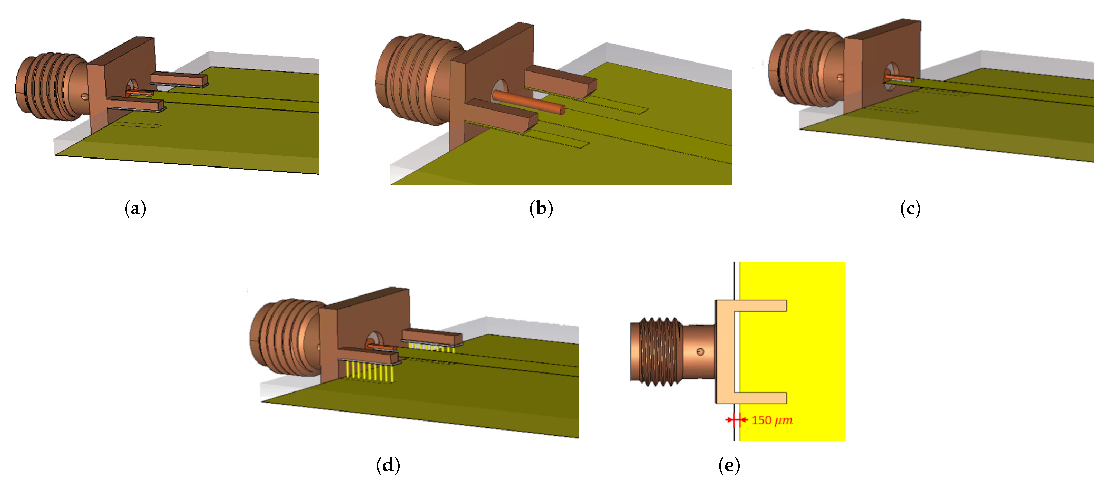
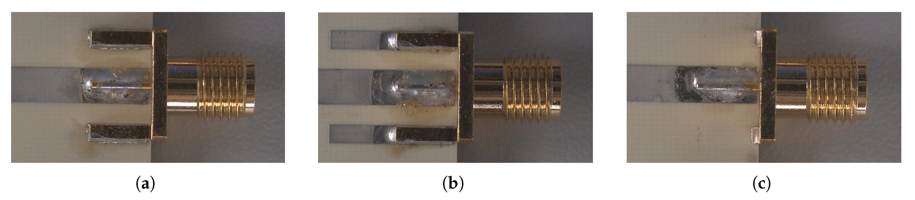
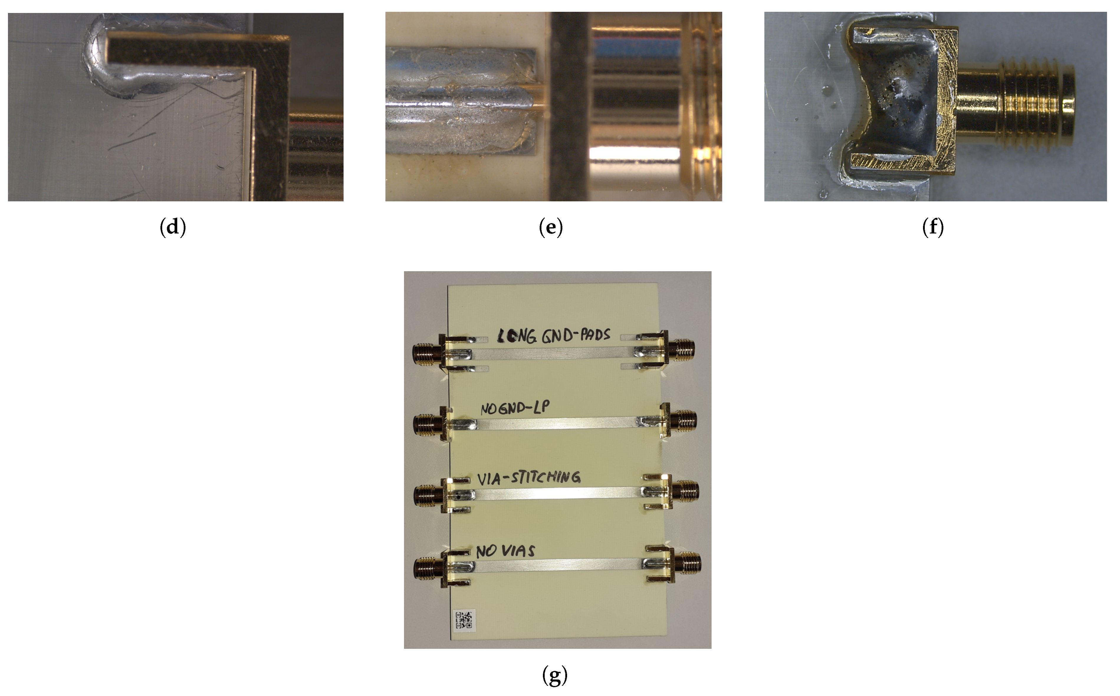
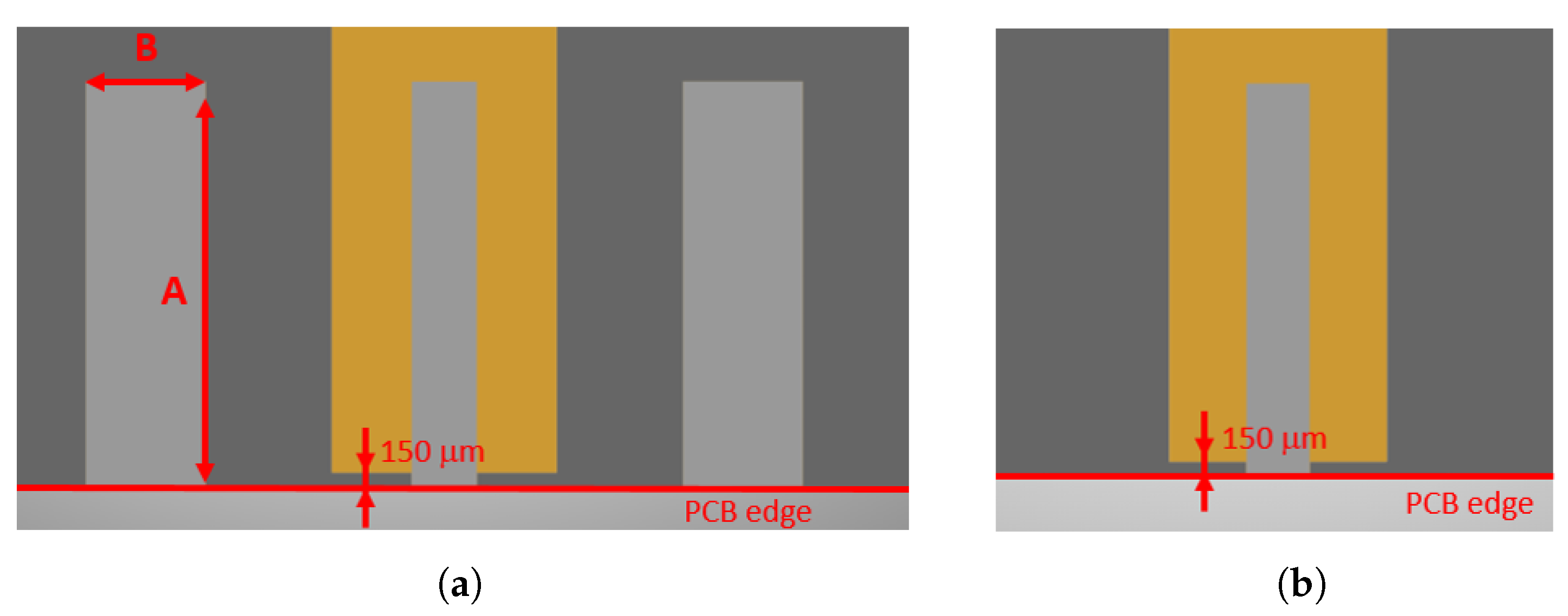
2. PCB Test Boards for Signal Launching Investigations

Figure 1 depicts the PCB test boards used in this work. Various signal launches for SMA edge mount connectors are designed to investigate various phenomena which deteriorate the performance of SMA-to-planar interfaces. First, a very simple PCB design (PCB 1) is considered (Figure 1a), where no measures are taken to overcome excess insertion losses at the interface. The PCB design comprises a microstrip line at the top layer and a large ground plane covering the bottom layer (Figure 1d). Additionally, landing pads for the SMA connector are placed on the top layer (Figure 2a). The design omits vias connecting the top ground pads with the bottom ground. The second design (PCB 2) uses the same microstrip structure as the first except that the length of the top landing pads for the SMA connector is increased (Figure 1b). The third PCB design (PCB 3) omits the top ground landing pads and corresponding pins are removed from the connector (Figure 1c). The experiments with PCB designs 1, 2 and 3 are considered to analyze the impact of the top ground landing pads on the performance of the signal launch. The designs intentionally violate the common practice design rules for RF PCB designs. However, the obtained results from these PCB structures provide fundamental information regarding EM field resonances occurring in the launching zone. Finally, a fourth PCB design (PCB 4) considers common RF PCB design guidelines. PCB 4 uses the same launching zone design as PCB 1 including vias connecting the top ground pads with the bottom ground layer. All four PCB designs use a high frequency substrate (RO4350B) which is characterized very accurately up to 50 GHz [16]. As indicated in [16], the dielectric constant ( ε r ) varies less than 1.5% from 1 GHz up to 50 GHz, hence a constant value of ε r = 3.66 (nominal value in data sheet) is used through out this work. Furthermore, the designs consider a spacing of 150 μm between PCB edge and conducting structures, as depicted in Figure 1d,e. This gap is often required by manufacturers to avoid broken metal structures during the cutting process of the PCB [17]. Therefore, an experiment is conducted to investigate the impact of this gap on the insertion and transmission losses. For this experiment the bottom ground metal is soldered to the SMA connector body by using a considerable amount of solder, as depicted in Figure 1f. The geometry and material parameters are summarized in Table 1. Utilizing the analytic equations from [18] for a microstrip line with the parameters from Table 1, one obtains a characteristic impedance of 52.41 Ω . This value was chosen intentionally different from 50 Ω to consider a small nominal impedance jump between the coaxial line and the microstrip line.

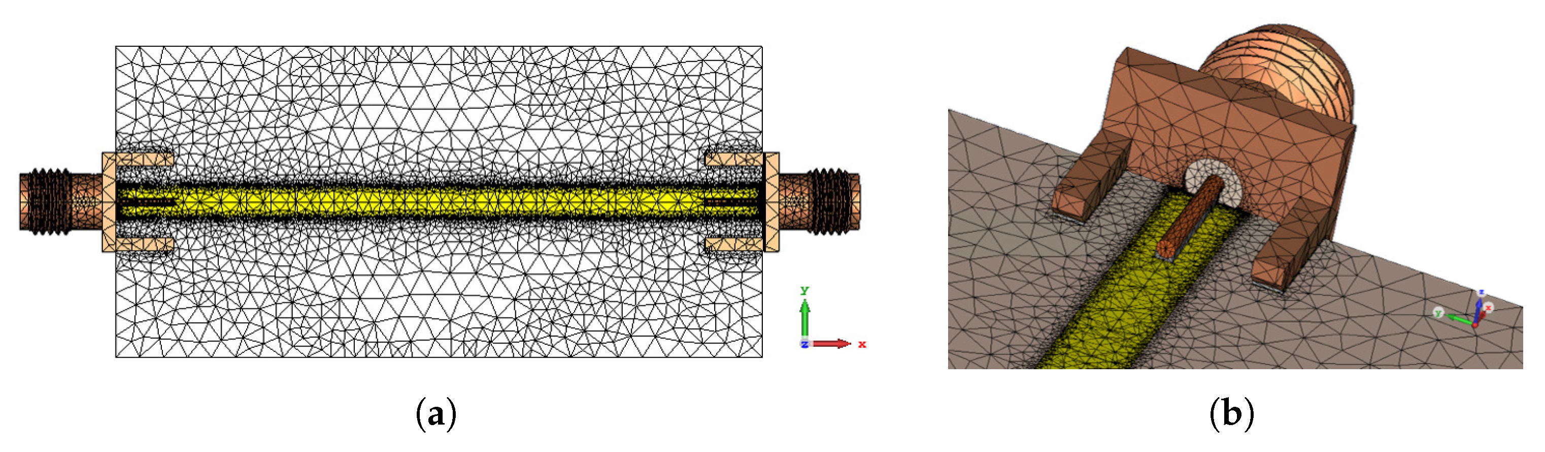
3. 3D Numerical Models of Test PCBs

This section describes the developed 3D numerical models which are used to identify the physical origin of excess transmission losses occurring in the S-Parameter measurements. The models were developed using the geometry values and material parameters of Table 1 and they are depicted in Figure 3a–d. The 3D numerical model for the SMA connector was provided by Würth Elektronik [3] and the material parameters for the connector are summarized in Table 2. It has turned out that the isolation material which is made of Polytetrafluoroethylene (PTFE) has a very strong impact especially in the low frequency domain. PTFE exhibits a small relative permittivity of about ε r = 2.1 [19]. Applying this relative permittivity value to the SMA connector model results in a characteristic impedance of 48.9 Ω [18]. However, as shown in Figure 4 for PCB 1, a characteristic impedance of 48.9 Ω within the SMA connector leads to increased reflections compared to the measurement for frequencies up to 4 GHz (more than 20 dB). Therefore, the relative permittivity of the PTFE material was adopted to ε r = 1.55 which would lead to a characteristic impedance of 55.6 Ω and a mismatch between SMA connector and the stripline. The value of ε r = 1.55 might be explained due to additional composites within the PTFE material. As shown in [19], hollow silica microspheres (HSM) might be introduced as fillers in the PTFE material to reduce its relative permittivity. Nevertheless, as shown later in the result section, by modifying ε r of the SMA insulator material, one obtains excellent agreement between the simulation and the measurement results up to 26 GHz.
To reduce the computation complexity of the numerical simulations the four PCB designs were investigated separately, although they are placed on one PCB, as depicted in Figure 1g. The distance between the single designs is 20 mm and numerical results revealed that the coupling between neighbouring designs is less than −25 dB up to a frequency of 26 GHz.

4. Results and Discussion

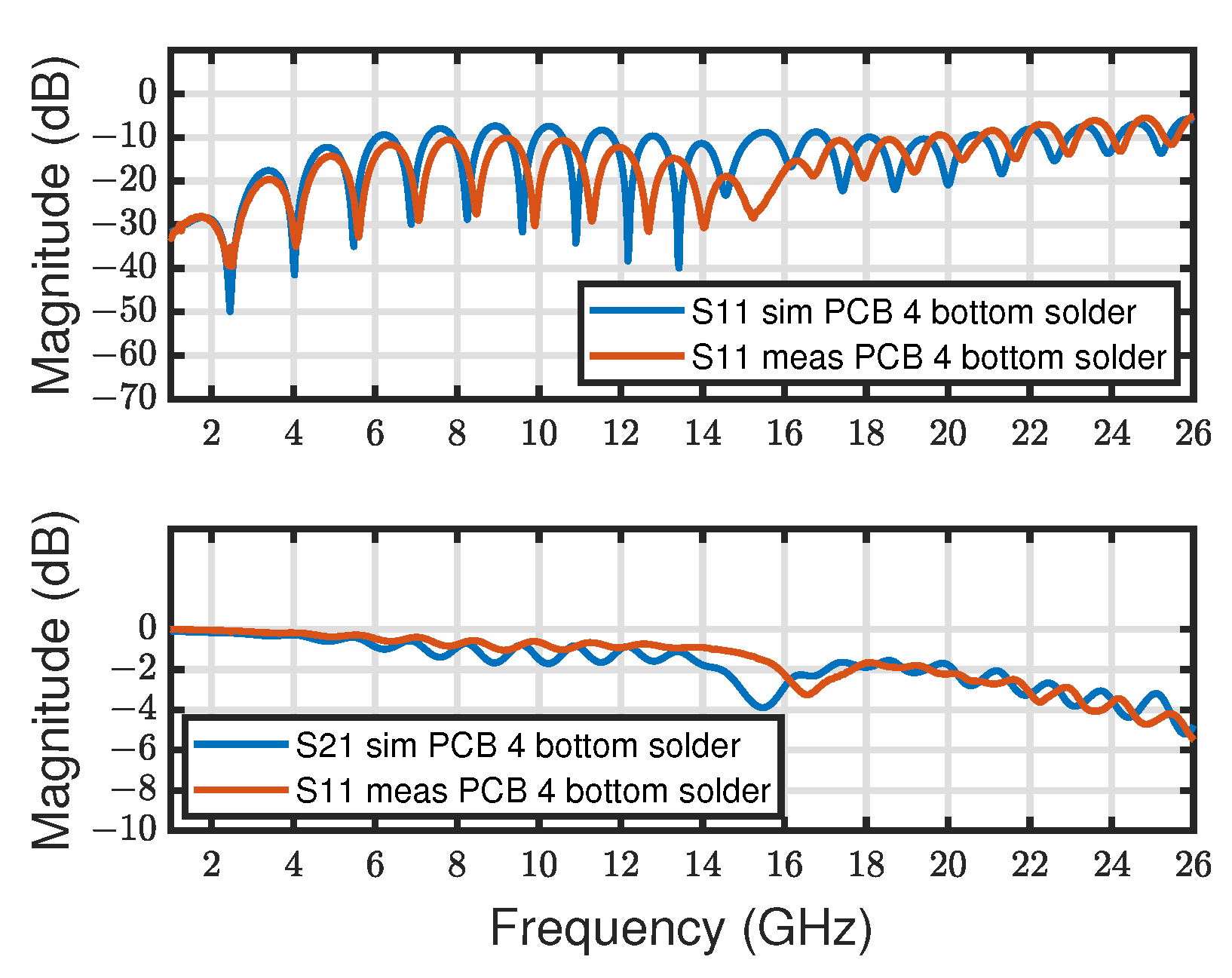
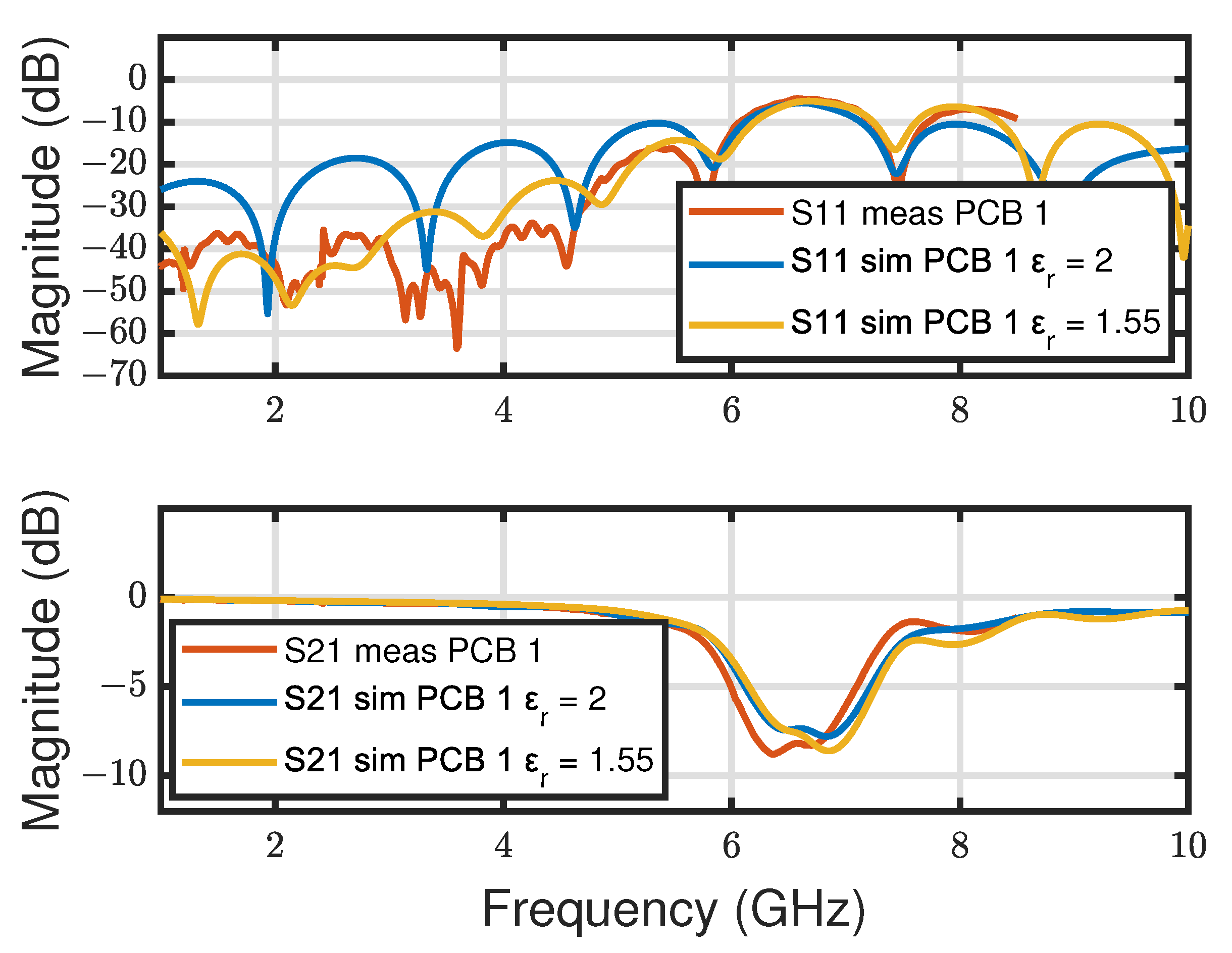
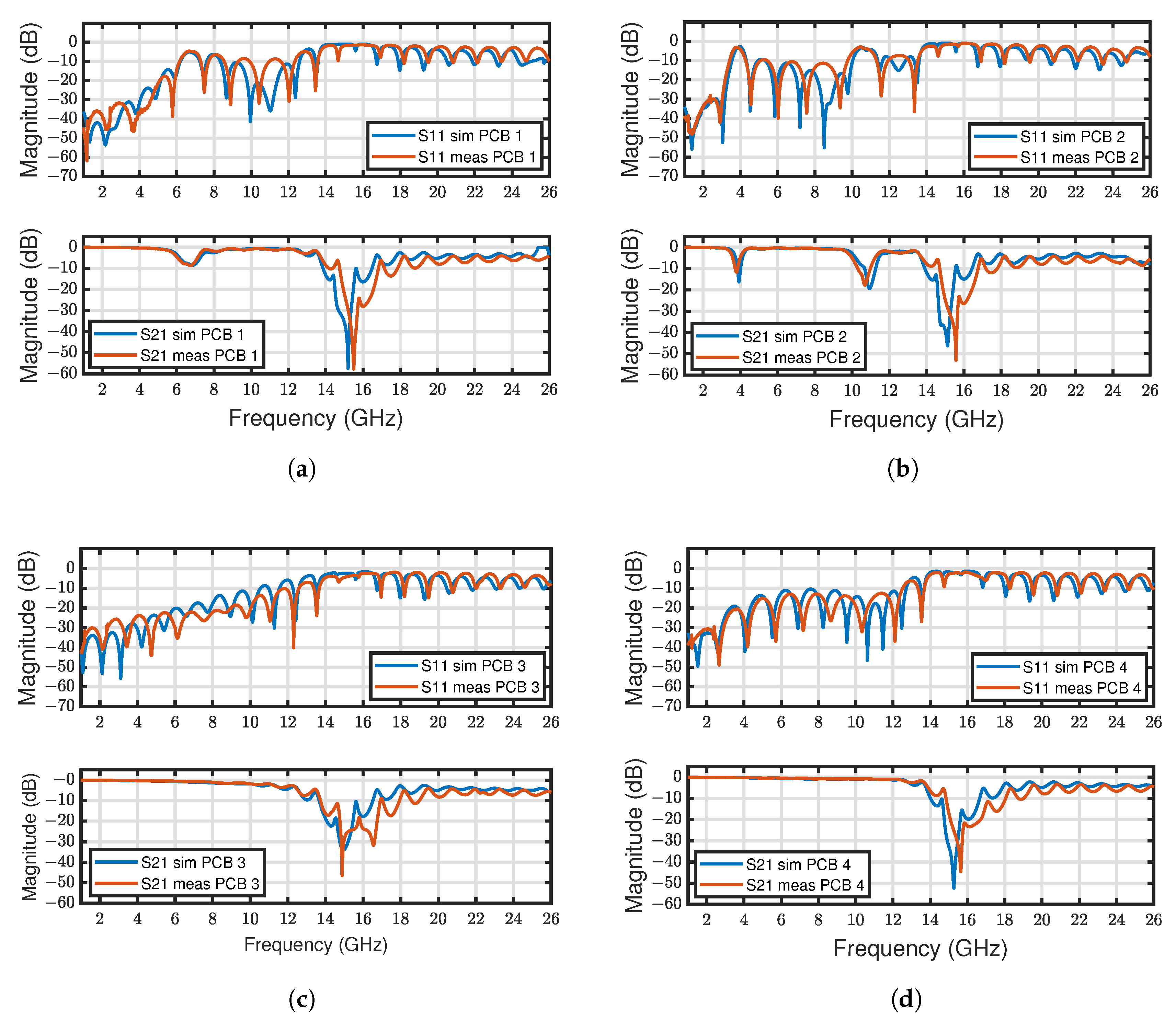
4.1. VNA Measurement

The simulation and measurement results for PCB 1, PCB 2, PCB 3 and PCB 4 are depicted in Figure 5 and Figure 6. The results comprise the insertion and transmission losses of the four investigated PCB designs up to 26 GHz. The measurement results were obtain utilizing the VNA Keysight PNA-X N5244B. As one can see, at 3.782 GHz, 6.85 GHz and 15.2 GHz increased transmission losses are present, resulting in increased reflections at the interface. At 3.782 GHz and 6.85 GHz, the insertion losses of the design omitting vias, are 12 dB and 7 dB, respectively, higher compared to the other two designs. Furthermore, also the reflection coefficient is about 8 dB higher, hence a deterioration of the performance in terms of signal integrity must be assumed. However, analyzing S-Parameters only provides little information regarding the physical origin of such a performance deterioration, hence additional investigations are required.

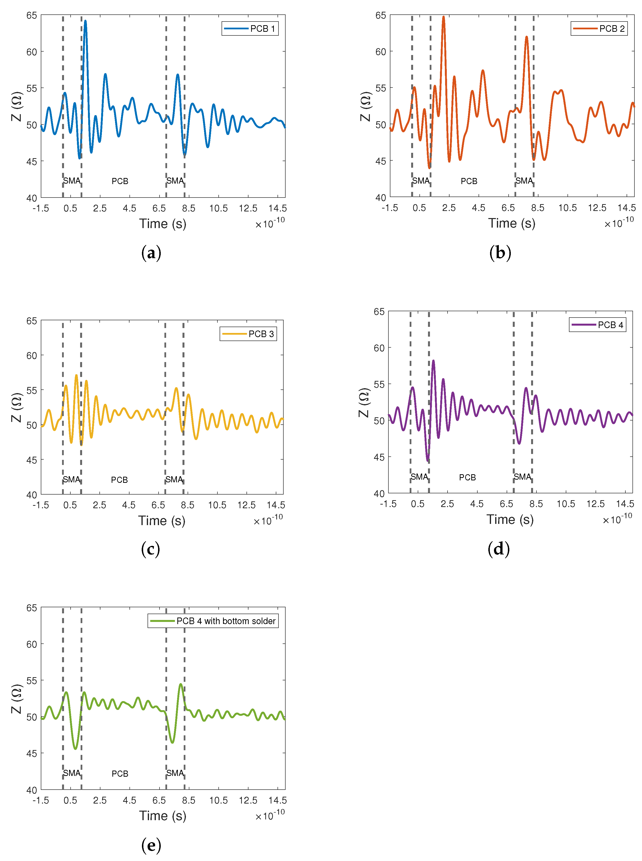
4.2. TDR Measurement

To identify the location of excess losses TDR measurements of all PCB designs were performed, as depicted in Figure 7. The TDR measurements were conducted using the Oscilloscope R&S RTP164 from Rhode and Schwarz with a band width of 16 GHz. As one can see in Figure 7, the impedance characteristic along the PCB varies enormous between the different designs. PCB 1 and PCB 2 exhibit an impedance jump up to 64.5 Ω which explains significant insertion losses observed in the S-Parameters. PCB 3 and PCB 4 exhibits an impedance jump up to 58 Ω and 56 Ω , respectively. Therefore, lower insertion losses can be observed, as shown in Figure 5. Finally, PCB 4 using solder at the bottom layer exhibits the lowest impedance jump at the interface, hence the losses can be further reduced.
Considering Figure 7e, one can see that the two SMA connectors are located at t 1 = 0 s and t 2 = 0.696 ns and they have a duration of T S M A = 0.124 ns. This time duration can be translated into a geometrical length as follows
l = c ε r μ r T 2
where c is the speed of light in vacuum and T is the time duration observed in the TDR measurement. The parameters ε r and μ r are the relative permittivity and the relative permeability, respectively. The duration between the end of the first SMA connector and the beginning of the second one is T P C B = 0.573 ns. Considering the PCB parameter values from Table 1, one obtains an effective relative permittivity of ε r e f f 1 = 2.84 [18]. Therefore, substituting ε r e f f 1 = 2.84 and T P C B = 0.573 ns into (1), one obtains a geometrical length of l P C B = 51 mm for the PCB which agrees with the actual PCB length between the SMA connectors since both connector overlap 5.6 mm with the PCB ( l P C B = 60 mm − 2 × 5.6 mm = 48.8 mm). At the interface one has to consider two different propagation speeds ( c ε r μ r ). First, within the SMA connector ε r 1 = 1.55, as discussed above. Second, at the transition region the coaxial mode within the connector changes to a planar mode at the PCB, hence a different relative permittivity is observed. We presume that the transition region exhibits ε r e f f 2 = 2.84. Finally, the geometrical length of the two SMA connector parts can be calculated from the TDR measurements as follows
l 1 , S M A l 2 , S M A = ε r e f f 2 ε r 1 T 1 , S M A T S M A T 1 , S M A
where l 1 , S M A and l 2 , S M A are the length of the coaxial part and the length of the planar part of the SMA connector, respectively. The parameter T S M A describes the duration of the complete SMA connector observed in the TDR measurement and T 1 , S M A is the duration of the coaxial part of the connector. Rearranging Equation (2) in terms of T 1 , S M A one obtains
T 1 , S M A = T S M A l 1 , S M A ε r 1 l 1 , S M A ε r 1 + l 2 , S M A ε r e f f 2
and
T 2 , S M A = T S M A T 1 , S M A
which allows us to separate the duration of the SMA connector parts. The values l 1 , S M A = 8.89 mm and l 2 , S M A = 5.6 mm are given in the data sheet and these values lead to a time duration of T 1 , S M A = 0.0669 ns and T 2 , S M A = 0.0571 ns in the TDR.
Nevertheless, as shown in Figure 7a–d it might be difficult to located the SMA connector accurately in the TDR measurement but it is a very powerful method to track the impedance change along the direction of propagation to identify the location of potential issues.

4.3. Measurement Summary

S-Parameter investigations are very powerful to characterize RF signal launches in terms of insertion and transmission losses. However, they do not provide any information regarding the location of these losses. To identify the location of potential issues TDR measurements may be used. However, no fundamental explanation regarding the physical origin of these issues can be derived from such measurements. Therefore, comprehensive EM field investigations are required to provide a fundamental understanding of the observed excess losses.

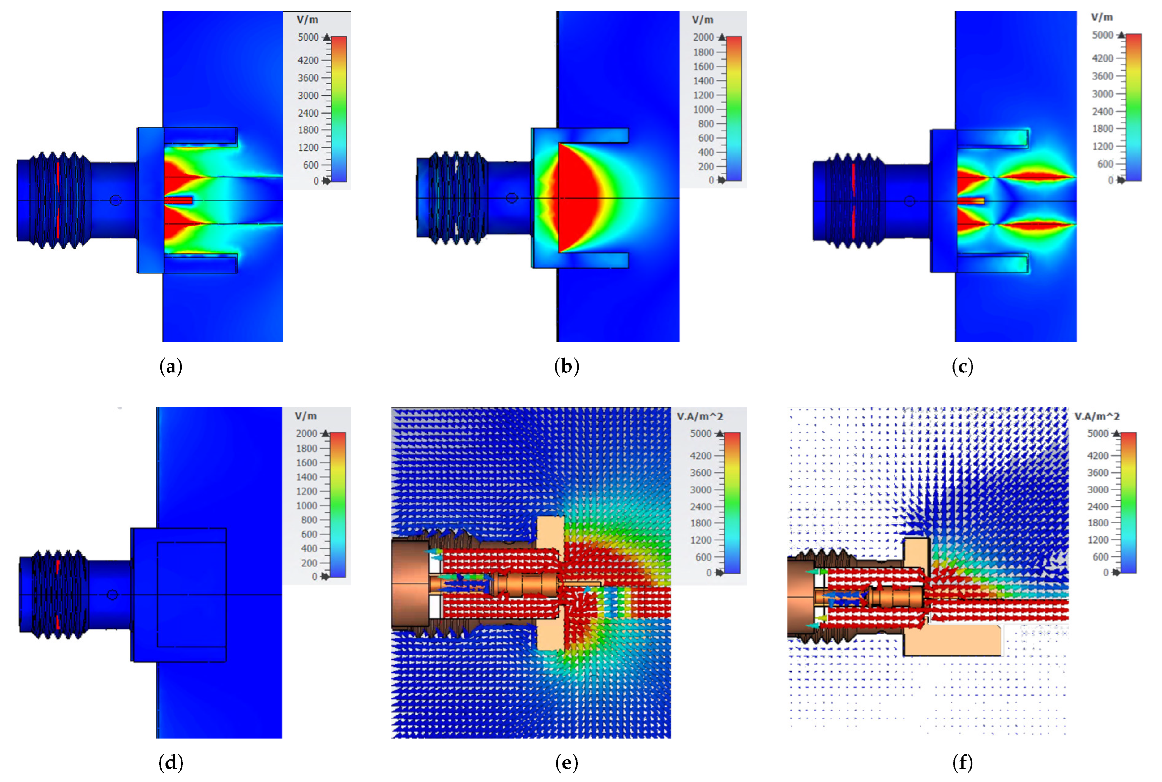
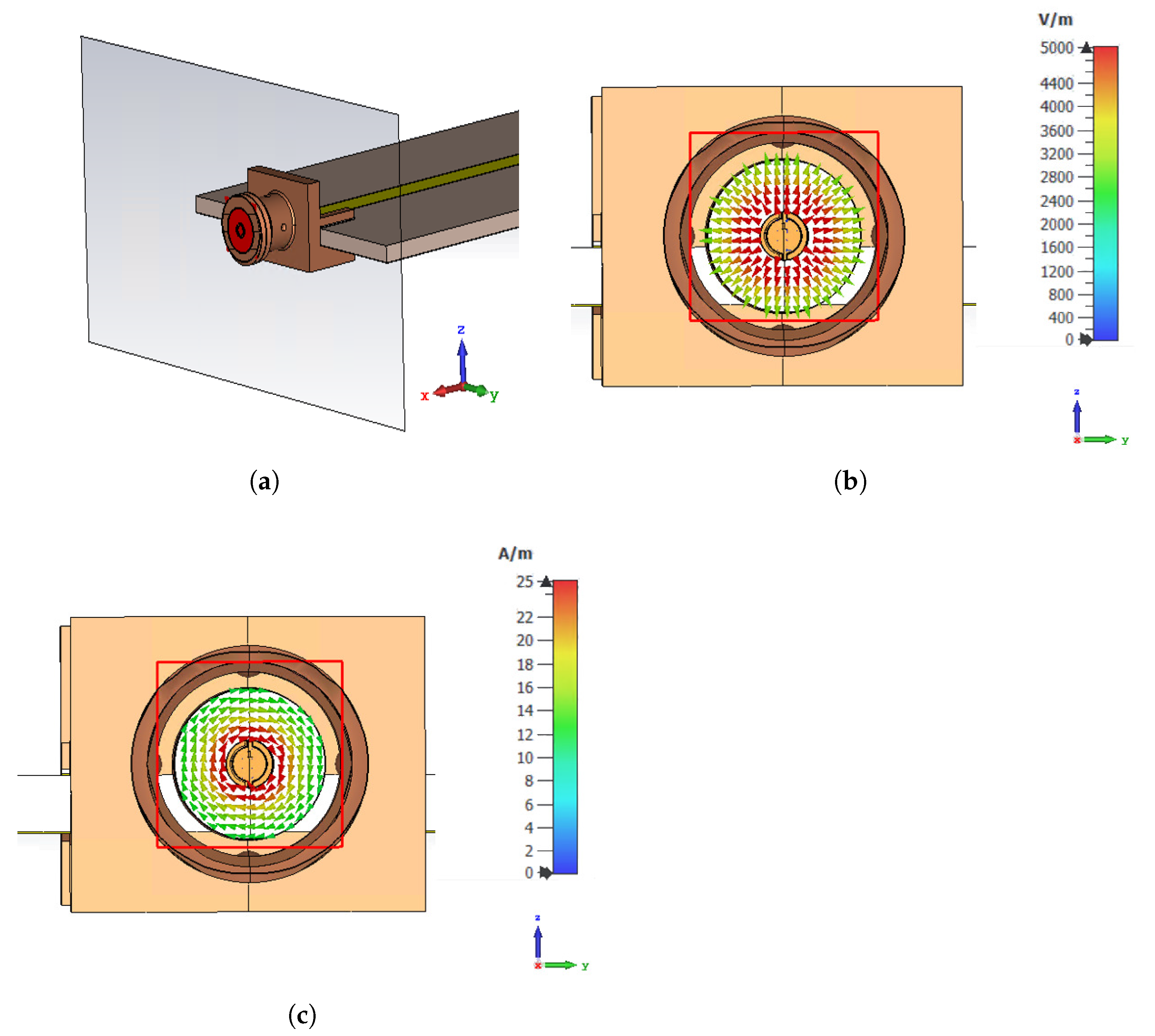
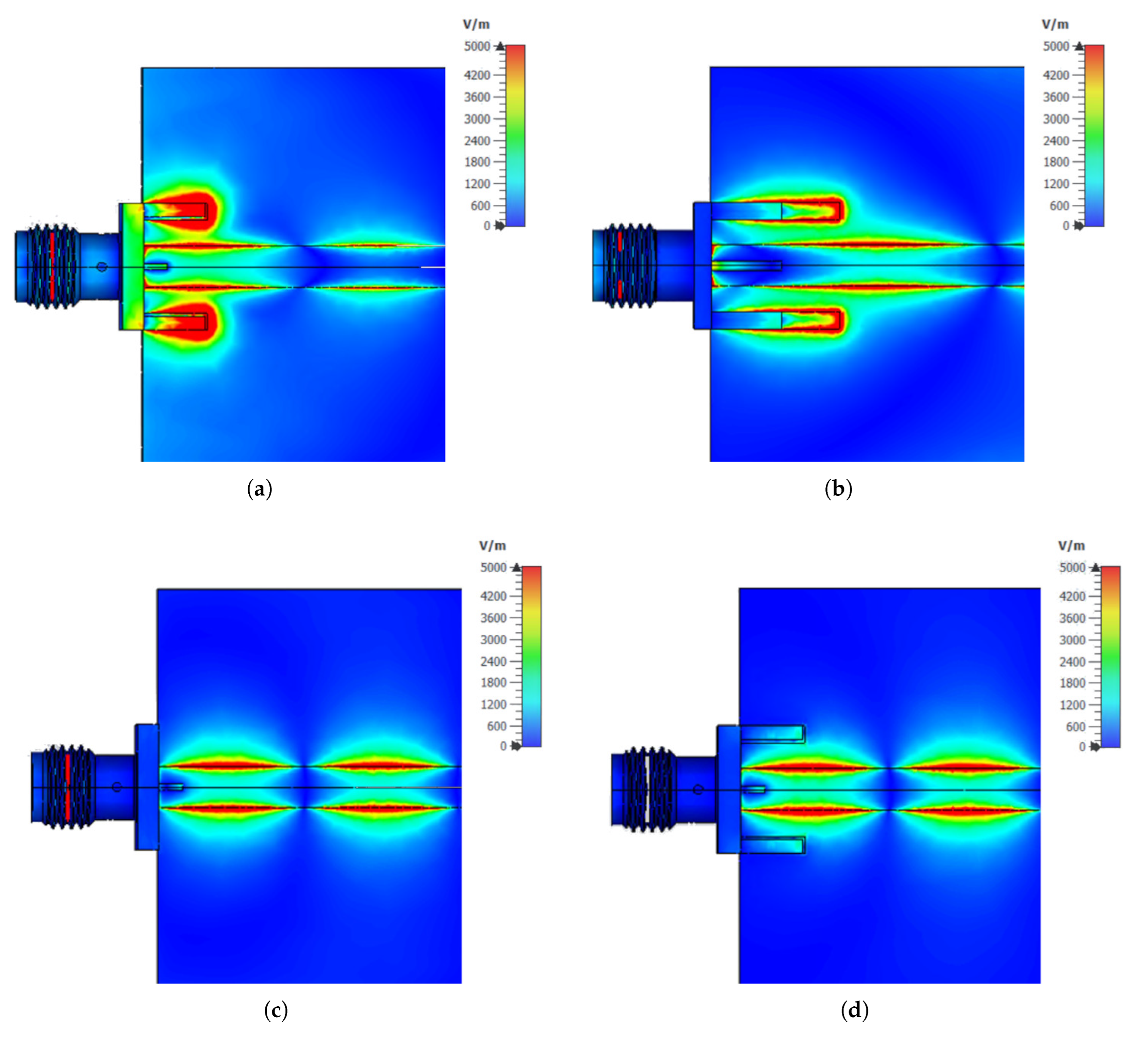
4.4. Simulation and EM Field Analysis

The results presented in this section are obtained by utilizing the finite-element-method (FEM) using tetrahedral mesh cells, as depicted in Figure 8. The excitation is located within the SMA connector, prescribing a coaxial wave guide, as depicted in Figure 9. Considering the results from Figure 10, the dominant source of excess transmission losses might be located at the SMA-to-microstrip interface, hence special attention was paid to discretize the critical region properly, see Figure 8b.
As discussed in [20], the Poynting’s theorem in its differential form can be represented as follows
S = E × H
· S = E · J + E · D t + H · B t
where S is the Poynting vector describing the power flow, E is the electric field intensity, D is the electric flux density and J is the conduction current density. H and B are the magnetic field intensity and magnetic flux density, respectively. Transforming Equation (6) into the frequency domain for an isotropic medium in which D = ε r ε 0 E and B = μ r μ 0 H one obtains
· S = E · J + j ω E · ε r ε 0 E + j ω H · μ r μ 0 H
and for a lossy dielectric medium one can define a complex permittivity [20]
ϵ r = ε r j ε r
where ε r describes the losses within the dielectric medium. Substituting Equation (8) into Equation (7) one obtains
· S = E · J + j ω ε 0 E · ( ε r E j ε r E ) + j ω H · μ r μ 0 H
· S = E · J + ω ε 0 ε r E · E + j ω ε 0 ε r E · E + j ω H · μ r μ 0 H
where the first term on the right-hand side describes the power dissipation caused by conduction currents ( J = σ E ) and the second term on the right-hand side describes the polarization losses occurring within the dielectric medium. Equation (10) assumes that no magnetic losses are present, hence one can derive
P l o s s = σ E · E + ω ε 0 ε r E · E
where P l o s s describes the total losses within conductor and dielectric medium.
Considering Equation (11) and the electric field distribution at 6.85 GHz, as depicted in Figure 10, one can explain the origin of the excess transmission losses observed at this frequency. As one can see in Figure 10a, the floating top ground pads cause a resonance of the electric field, hence increased losses are occurring. To confirm the origin of these losses another experiment was conducted where the length of the top ground pads is increased (PCB 2). The results for PCB 2 are depicted in Figure 10b. As one can see, the frequency where excess transmission losses are observed is shifted to a lower frequency value (3.782 GHz). Therefore, it can be concluded that the frequency of these transmission losses is determined by the length of the top ground metal. To overcome the problem of signal deterioration below 10 GHz the designs for PCB 3 and 4 are considered. The electric field distributions for these designs are presented in Figure 10c,d. As depicted, PCB 3 and 4 do not exhibit an electric field resonance, therefore there is no performance deterioration observed. From the obtained results one can conclude that floating ground connections must be avoided to improve the signal launch design. The best results in terms of insertion and transmission losses were obtained by connecting the top and bottom ground metals using vias which confirms the reported RF design guidelines presented in [14].
Additional to the excess transmission loss at 6.85 GHz, another frequency of excess transmission loss is observed at 15.2 GHz, as depicted in Figure 5. These losses can be attributed to the gap between the PCB edge and the ground metal at the bottom layer, as indicated in Figure 11b. The gap causes a resonance of the electric field, hence considering Equation (11) additional losses are present. The power flow of the SMA-to-microstrip interface is depicted in Figure 11e. By shorting the gap between PCB edge and bottom ground by using a solid tin metal block, one can see that the electric field resonance disappears (Figure 11d), hence an improvement of the performance can be observed, as depicted in Figure 6. This observation is confirmed by investigating the power flow, as depicted in Figure 11f. When a continuous ground connection is established between the SMA connector and the PCB, the second source of excess transmission losses at 15.2 GHz can be prevented. This observation matches the results reported in [4]. The authors in [4], introduce edge plating to overcome the ground discontinuity issues but as shown in Figure 11, it is sufficient to short the gap between SMA connector and PCB ground metal by applying solder in this region. Establishing a continuous ground connection does not only suppress excess transmission losses but also reduces the insertion losses above 18 GHz by approximately 10 dB, as shown in Figure 6e.

4.5. EM Field Analysis Summary

The presented results in the previous section identify the physical origin of excess losses at various frequencies due to EM field resonances. Two effects were identified as the dominant loss mechanisms in the frequency range of interest. Firstly, top and bottom ground metal structures on PCBs must be connected by using vias otherwise electric field resonances occur resulting in excess losses below 10 GHz. Secondly, ground discontinuities at the SMA-to-microstrip interface cause significant field leakage resulting in excess losses at 15.2 GHz. Therefore, a continuous ground connection along the direction of propagation must be ensured by applying solder across the whole gap between the SMA connector and PCB bottom ground.

5. Conclusions

In this paper, we presented a comprehensive EM field investigation of SMA-to-microstrip interfaces to locate and suppress the sources of excess losses. As we have shown many different factors must be considered during the development of a high performance RF measurement PCB. Small design features may have a significant influence on insertion and transmission losses, hence this work focused on the identification of its physical origins. The presented results are intended to assist RF PCB designers to understand the basic principles of EM field theory and their impact on signal deterioration. S-Parameter results are versatile in their applicability and most of the scalar quantities of interest, e.g., input impedance can be extracted using post-processing. However, they do not provide any information in identifying issues within a PCB design. Therefore, an RF PCB designer should always be aware of the EM fields and power flow to identify potential issues which may occur within a PCB design.

Author Contributions

Conceptualization, C.R. and T.B.; methodology, C.R.; software, C.R.; validation C.R. and H.H.; formal analysis, C.R.; investigation, C.R., S.K. and K.R.; writing—original draft preparation, C.R.; supervision, T.B.; funding acquisition, M.K. and T.B. All authors have read and agreed to the published version of the manuscript.

Funding

This research received no external funding.

Acknowledgments

This work has been supported by the “University SAL Labs” initiative of Silicon Austria Labs (SAL) and its Austrian partner universities for applied fundamental research for electronic based systems. We thank Dassault Systémes Simulia Corp. for providing us their software SIMULIA CST Studio Suite. Supported by TU Graz Open Access Publishing Fund.

Conflicts of Interest

The authors declare no conflict of interest.

References

  1. Wadell, B.C. Transmission Line Design Handbook, 1st ed.; Artech House, Inc.: Norwood, MA, USA, 1991; pp. 479–481. [Google Scholar]
  2. Shoaib, N. Vector Network Analyzer (VNA) Measurements and Uncertainty Assessment, 1st ed.; Springer: Cham, Switzerland, 2017; pp. 1–55. [Google Scholar]
  3. WR-SMA Round Post for PCB 1.6 mm. Available online: https://www.we-online.com/katalog/de/ROUND_POST_FOR_PCB_1_6_M_M (accessed on 19 January 2022).
  4. Stavoli, R.; Correia, D.; Soubh, E. Demystifying Edge Launch Connectors. Signal Integr. J. 2019. Available online: https://www.signalintegrityjournal.com/articles/1094-demystifying-edge-launch-connectors (accessed on 19 January 2022).
  5. Almuqati, N.; Sigmarsson, H. 3D Microstrip Line Taper on Ultra-low Dielectric Constant Substrate. In Proceedings of the 2019 IEEE 20th Wireless and Microwave Technology Conference (WAMICON), Cocoa Beach, FL, USA, 8–9 April 2019. [Google Scholar]
  6. Gupta, S.; Sebak, A.R.; Devabhaktuni, K.D. Optimum Launch-Taper Matching Technique for mm-Wave Applications. In Proceedings of the 2017 IEEE MTT-S International Microwave and RF Conference (IMaRC), Ahmedabad, India, 11–13 December 2017. [Google Scholar]
  7. Drak, O.T.; Liubina, M.L. Coaxial to Microstrip Transition Matching Method. In Proceedings of the 2021 IEEE Conference of Russian Young Researchers in Electrical and Electronic Engineering (ElConRus), St. Petersburg, Russia, 26–29 January 2021. [Google Scholar]
  8. Liang, H.; Laskar, J.; Barnes, H.; Estreich, D. Design and optimization for coaxial-to-microstrip transition on multilayer substrates. In Proceedings of the 2001 IEEE MTT-S International Microwave Sympsoium Digest (Cat. No.01CH37157), Phoenix, AZ, USA, 20–24 May 2001. [Google Scholar]
  9. Optimizing Test Boards for 50 GHz End Launch Connectors. Available online: https://mpd.southwestmicrowave.com/wp-content/uploads/2018/07/Optimizing-Test-Boards-for-50-GHz-End-Launch-Connectors.pdf (accessed on 19 January 2022).
  10. The Design and Test of Broadband Launches up to 50 GHz on Thin and Thick Substrates. Available online: https://www.hasco-inc.com/content/Technical_Articles/Design_and_Test_Broadband_Launches.pdf (accessed on 19 January 2022).
  11. Coonrod, J. Signal Launch Methods for RF/Microwave PCBs. Available online: https://www.signalintegrityjournal.com/articles/152-signal-launch-methods-for-rfmicrowave-pcbs (accessed on 19 January 2022).
  12. Ellison, J.; Smith, S.B.; Agili, S. Using a 2x-thru standard to achieve accurate de-embedding of measurements. Microw. Opt. Technol. Lett. 2020, 62, 675–682. [Google Scholar] [CrossRef]
  13. Stepins, D.; Asmanis, G.; Asmanis, A. Measuring Capacitor Parameters Using Vector Network Analyzers. Electronics 2014, 18, 29–38. [Google Scholar] [CrossRef] [Green Version]
  14. Coaxial PCB Connector PCB-Transmission Line Design Guide. Available online: https://www.we-online.com/catalog/media/o563287v410%20ANE012a%20EN.pdf (accessed on 11 March 2022).
  15. CST Studio Suite—Electromagnetic Field Simulation Software. Available online: https://www.3ds.com/products-services/simulia/products/cst-studio-suite/?utm_source=cst.com&utm_medium=301&utm_campaign=cst (accessed on 3 June 2022).
  16. RO4000 Laminates RO4003C and RO4350B—Data Sheet. Available online: https://rogerscorp.com/-/media/project/rogerscorp/documents/advanced-electronics-solutions/english/data-sheets/ro4000-laminates-ro4003c-and-ro4350b—data-sheet.pdf (accessed on 24 January 2022).
  17. Lischka, G. Design and Realization of Microstrip—Transitions up to 90 GHz. Master’s Thesis, Technical University of Vienna, Vienna, Austria, 2005. [Google Scholar]
  18. Paul, C.R. Introduction to Electromagnetic Compatibility (Wiley Series in Microwave and Optical Engineering, 2nd ed.; Wiley-Interscience: Hoboken, NJ, USA, 2006; pp. 199–204. [Google Scholar]
  19. Li, Y.; Zhou, J.; Shen, J.; Li, Q.; Qi, Y.; Chen, W.A. Ultra-low permittivity HSM/PTFE composites for high-frequency microwave circuit application. J. Mater. Sci. Mater. Electron. 2022, 33, 10096–10103. [Google Scholar] [CrossRef]
  20. Paul, C.R.; Nasar, S.A. Introduction to Electromagnetic Fields, 2nd ed.; Wiley-Interscience: Hoboken, NJ, USA, 1987; pp. 251–254. [Google Scholar]
Figure 1. (a) Test PCB 1 and PCB 4. (b) Test PCB 2. (c) Test PCB 3. (d,e) Test PCB 1, PCB 2, PCB 3 and PCB 4 top and bottom view with 150 μ m ground edge. (f) Solder at the bottom layer to connect the bottom ground metal with the SMA connector body. (g) Complete PCB design. The PCB is connected via coaxial cables to the VNA Keysight PNA-X N5244B.
Electronics 11 01990 g001aElectronics 11 01990 g001b
Figure 2. (a) PCB top view of signal launch used in PCB 1, PCB 2 and PCB 4. (b) PCB top view of signal launch used in PCB 3. The values for A and B are listed in Table 1.
Electronics 11 01990 g002
Figure 3. 3D models to investigate increased insertion and transmission losses at an SMA-to-microstrip interface. (a) PCB 1 model with ground metal at the top layer (no vias). (b) PCB 2 model with increased length of top ground metal (no vias). (c) PCB 3 with removed ground metal at the top layer. (d) PCB 4 with vias to connect the top and bottom ground. (e) bottom view of PCB designs (ad). All PBC designs use the same SMA connector model [3].
Electronics 11 01990 g003
Figure 4. Investigation of insertion and transmission losses for various values of ε r for PTFE applied to the SMA connector model.
Electronics 11 01990 g004
Figure 5. Comparison of insertion and transmission losses of different PCB designs (see Figure 3). (a) PCB 1; (b) PCB 2; (c) PCB 3; (d) PCB 4.
Electronics 11 01990 g005
Figure 6. Comparison of insertion and transmission losses of PCB 4 applying solder to connect the bottom ground metal with the SMA connector body (compare Figure 1f).
Electronics 11 01990 g006
Figure 7. (ad) Comparision of TDR measurements of PCB 1, PCB 2, PCB 3 and PCB 4. (e) TDR measurement of PCB 4 applying solder to short the PCB edge gap between the ground metal layer and the SMA connector body.
Electronics 11 01990 g007
Figure 8. Discretization of 3D models. (a) Discretization of complete PCB. (b) Discretization of SMA-to-microstrip interface.
Electronics 11 01990 g008
Figure 9. Coaxial excitation at the SMA connector. (a) Location of exciting wave guide port. (b) Prescribed E -field at excitation plane. (c) Prescribed H -field at excitation plane.
Electronics 11 01990 g009
Figure 10. Top view of E -field distribution at 6.85 GHz where increased losses can be observed. (a) E -field resonance occurring at 6.85 GHz in the PCB 1 model (Figure 3a). (b) E -field resonance of PCB 2 occurring at 3.782 GHz. The resonance is caused by the ground metal at the top layer. (c) E -field distribution after removing top ground metal (PCB 3, Figure 3c). (d) E -field distribution at 6.85 GHz using vias (PCB 4) to connect the top and bottom ground (Figure 3d).
Electronics 11 01990 g010
Figure 11. E -field distribution at 15.2 GHz where increased insertion and transmission losses can be observed. (a,b) top and bottom view of the E -field resonance occurring at 15.2 GHz. The resonance is caused by the gap between PCB board edge and bottom ground metal. (c,d) top and bottom view of the E -field distribution at 15.2 GHz using a solid tin block to connect the bottom ground metal to the SMA connector body. (e) side view of the Poynting vector at the SMA-to-PCB interface with a 150 μ m gap between PCB edge and bottom ground metal. (f) side view of the Poynting vector at the SMA-to-PCB interface using a solid tin block to overcome the ground discontinuity.
Electronics 11 01990 g011
Table 1. Geometry and material parameters used for the test PCBs. The parameters L and H describe the length and the height of the PCB designs. All four designs are placed on the same PCB with a distance of 20 mm between each other. The overall PCB outline is 60 × 100 mm. The parameters A and B describe the dimensions of the top ground landing pads (see Figure 2a). PCB 3 does not use top ground landing pads.
SubstrateRO4350B ( ε r = 3.66 ) [16]
L × H60 × 1.524 mm
Copper thickness44 μ m
Trace width3.1 mm
Signal launch (A × B)
PCB 15.5 × 1.65 mm
PCB 211 × 1.65 mm
PCB 30 × 0 mm
PCB 45.5 × 1.65 mm
Table 2. Material parameters used for the SMA edge mount connector [3].
Body materialBrass with σ = 2.74 × 10 7 S m
Center contact materialBeryllium-Copper with σ = 1.16 × 10 7 S m
Isolation materialPTFE with ε r = 1.55
Publisher’s Note: MDPI stays neutral with regard to jurisdictional claims in published maps and institutional affiliations.

