
A V2G Enabled Bidirectional Single/Three-Phase EV Charging Interface Using Modular Multilevel Buck PFC Rectifier

 ,
, 
 and
and 
Abstract
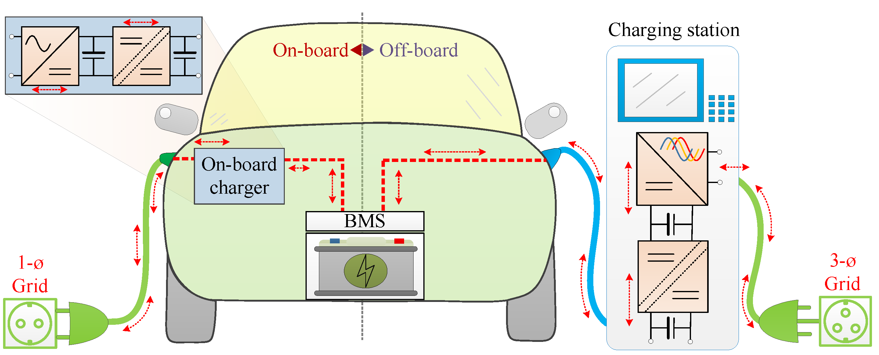
:1. Introduction
- A switched capacitors (SC) based bidirectional modular AC-to-DC buck PFC active rectifier; and
- A bidirectional DC-to-DC converter.
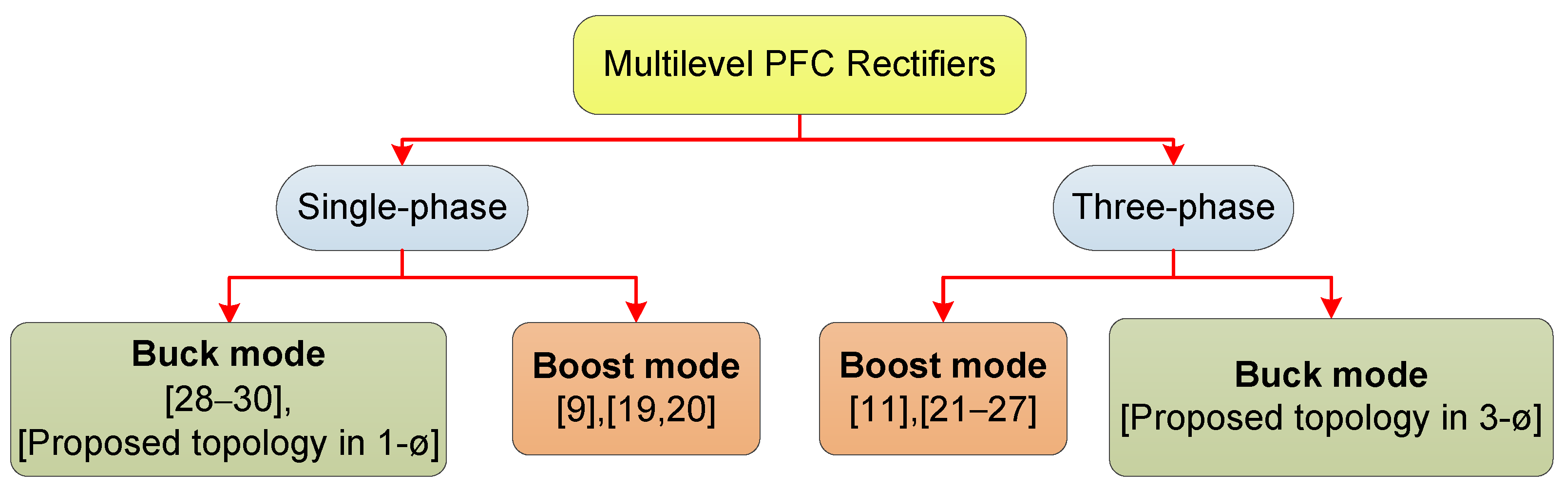
- The proposed topology can be easily structured for both the single-phase version (for on-board EV charging) and the three-phase version (for off-board EV charging);
- It operates in both V2G and G2V modes;
- It synthesizes seven levels at the line voltage, thereby considerably improving the harmonic profile. If needed, the modularity of the proposed structure allows further extension of the number of levels;
- Without using any complex control methods, only the output voltage needs to be balanced, and all other capacitors’ voltages are automatically balanced;
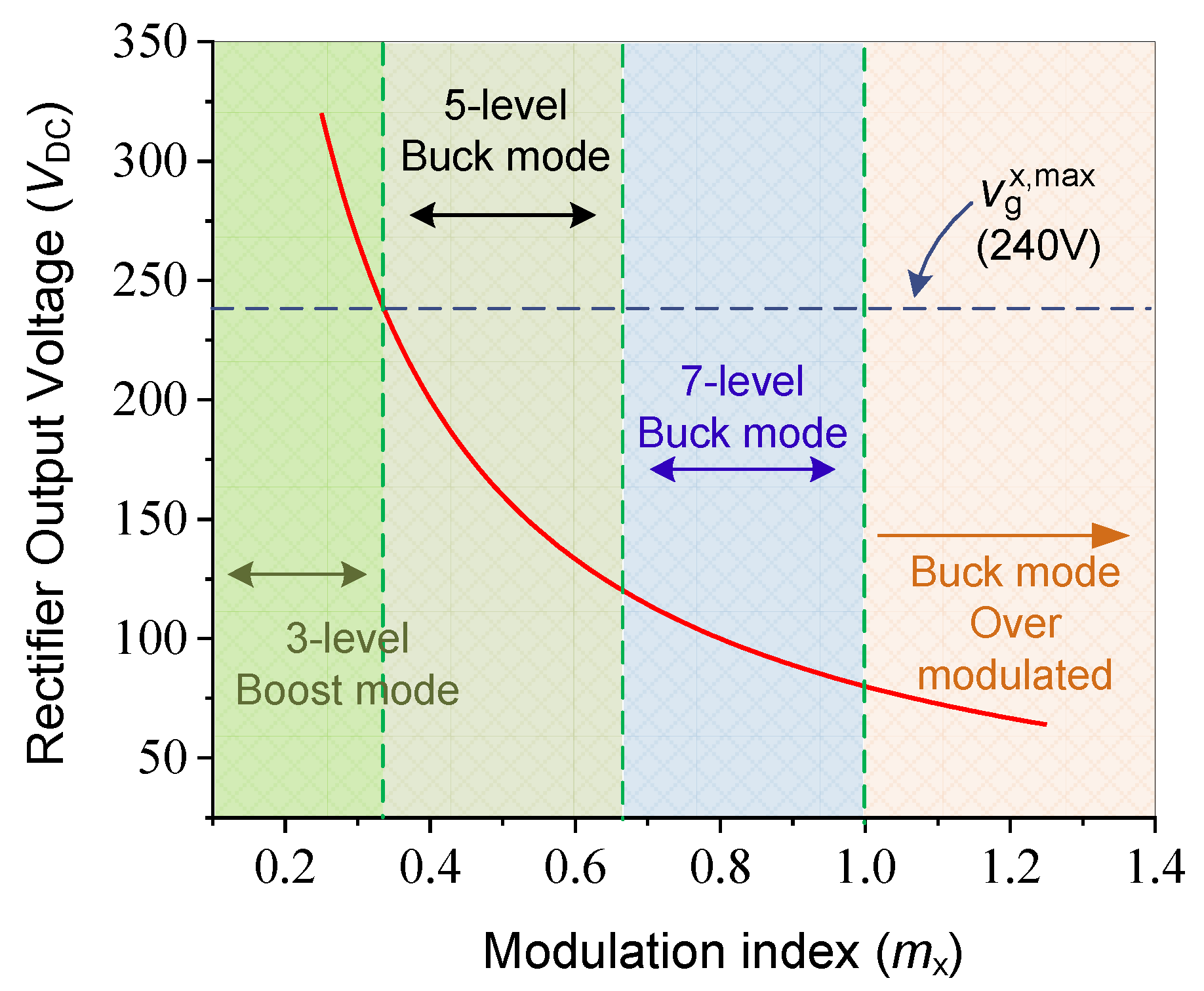
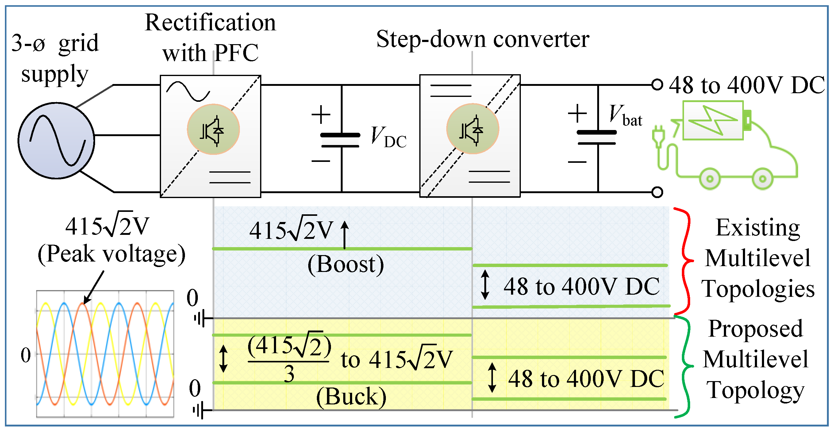
- It works in buck mode, with a wide output range; and
- It operates in continuous conduction mode, thereby eliminating the need for large filters.
2. Circuit Topology
- State 1 (Vxn = 0): During this state, the switches Sx2, Sx3, Sx5, Sx6 and Sx8 are turned ON, so as to achieve two simultaneous conduction paths, as shown in Figure 5a. In the path shown with red, it can be seen that all capacitors are bypassed, such that the voltage Vxn = 0. Additionally, for the path shown in green, the capacitors Cx1, Cx2 and Co are in parallel and maintain capacitor voltage to VDC.
- State 2 (Vxn = +VDC): During this state, the switches Sx1, Sx3, Sx5, Sx6 and Sx8 are turned ON, so as to achieve two simultaneous conduction paths, as shown in Figure 5b. In the path shown with red, it can be seen that the capacitor Co is in the path with terminal “x” and “n”, such that the voltage Vxn = +VDC. Additionally, for the path shown in green, the capacitors Cx1, Cx1 and Co are in parallel and balance the voltage of the capacitor to VDC.
- State 3 (Vxn = +2 VDC): During this state, the switches Sx1, Sx4, and Sx6 are turned ON, so to achieve conduction paths, as shown in Figure 5c. In the path shown with red, it can be seen that the capacitors Cx1 and Co are in the path with terminal “x” and “n”, such that the voltage Vxn = +2 VDC.
- State 4 (Vxn = +3 VDC): During this state, the switches Sx1, Sx4, and Sx7 are turned ON, so as to achieve conduction paths, as shown in Figure 5d. In the path shown with red, it can be seen that the capacitors Cx1, Cx2 and Co are series, such that the voltage Vxn = +3 VDC.
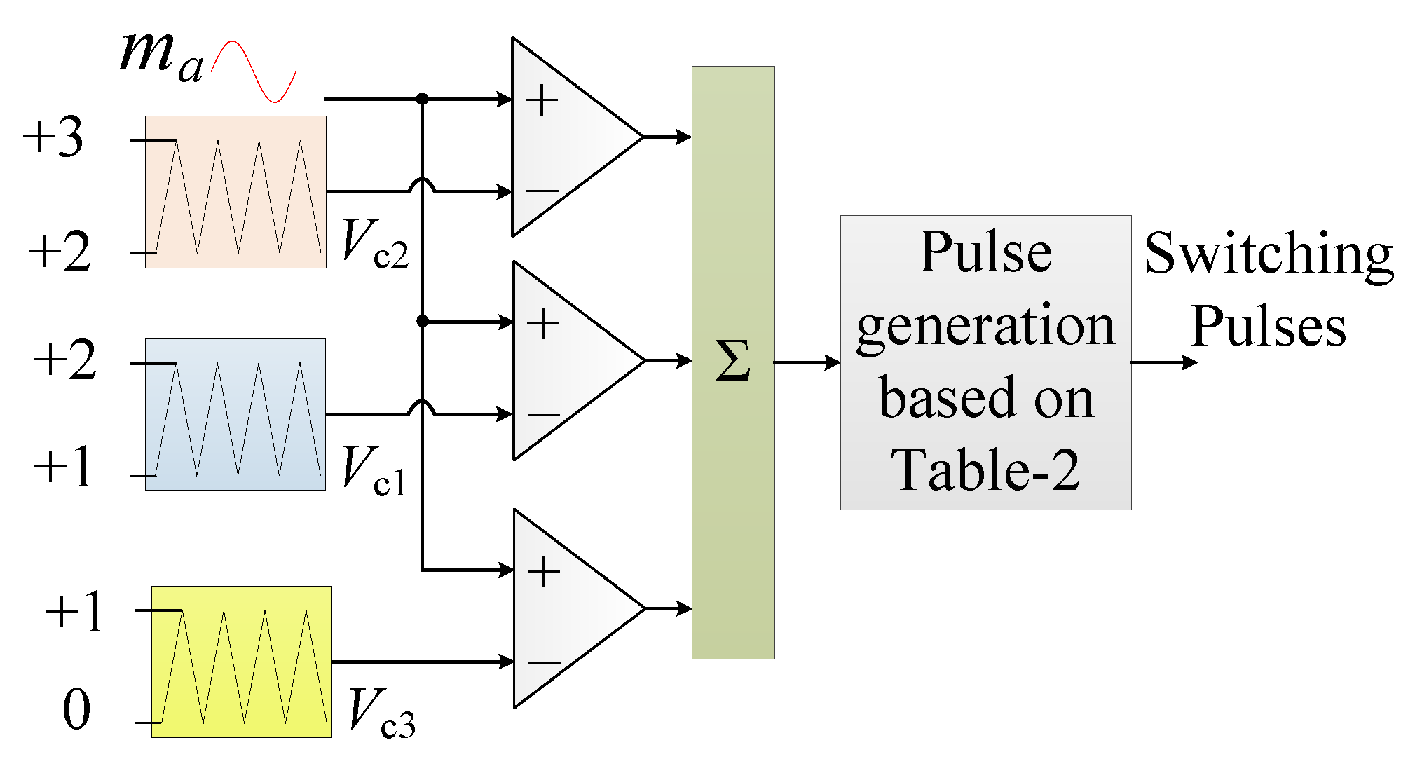
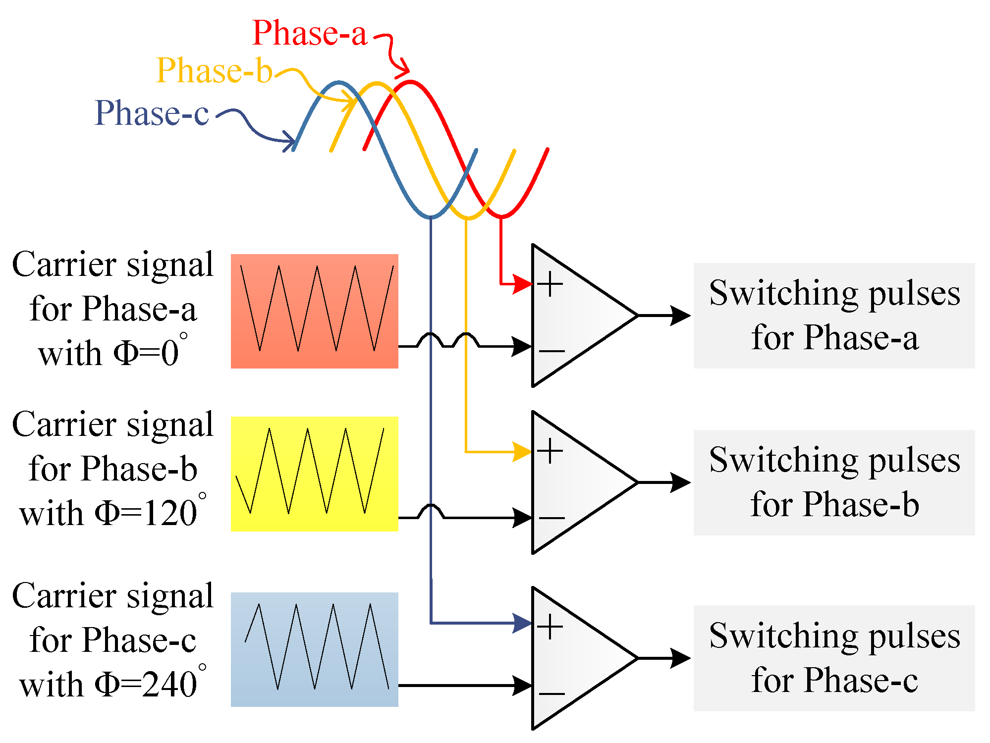
3. Modulation Scheme and Controller
3.1. Pulse Width Modulation (PWM) Scheme
3.2. Controller Design
4. Comparative Analysis with Existing PFC Rectifiers
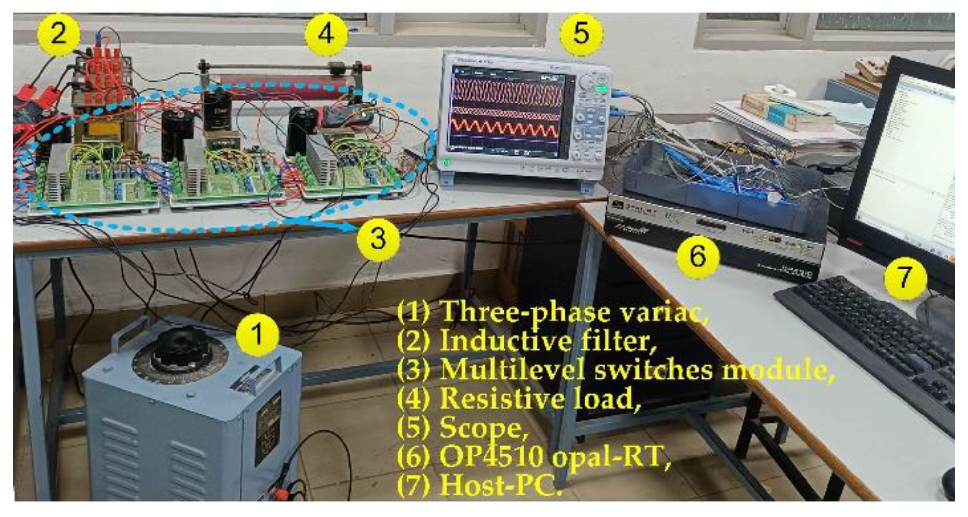
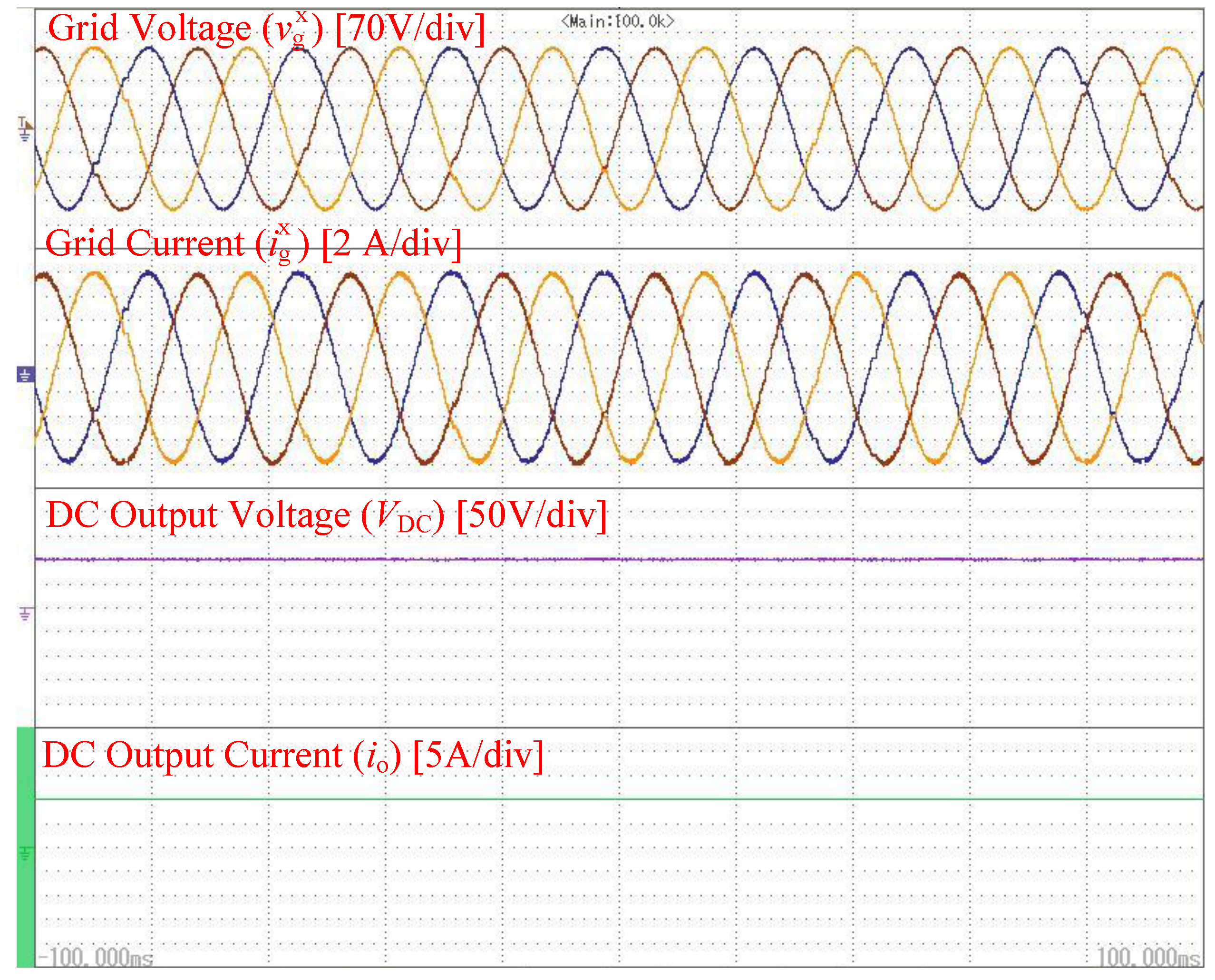
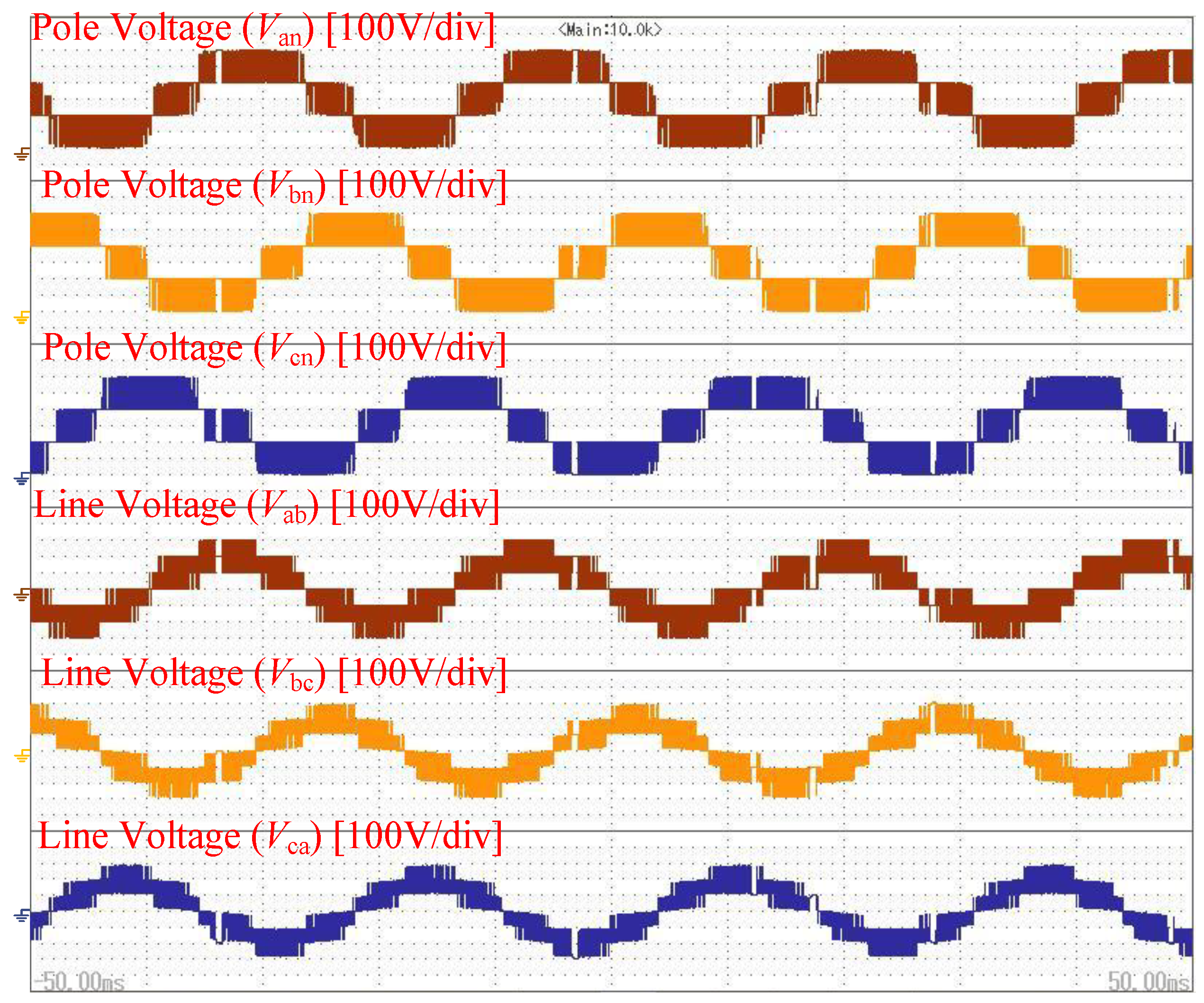
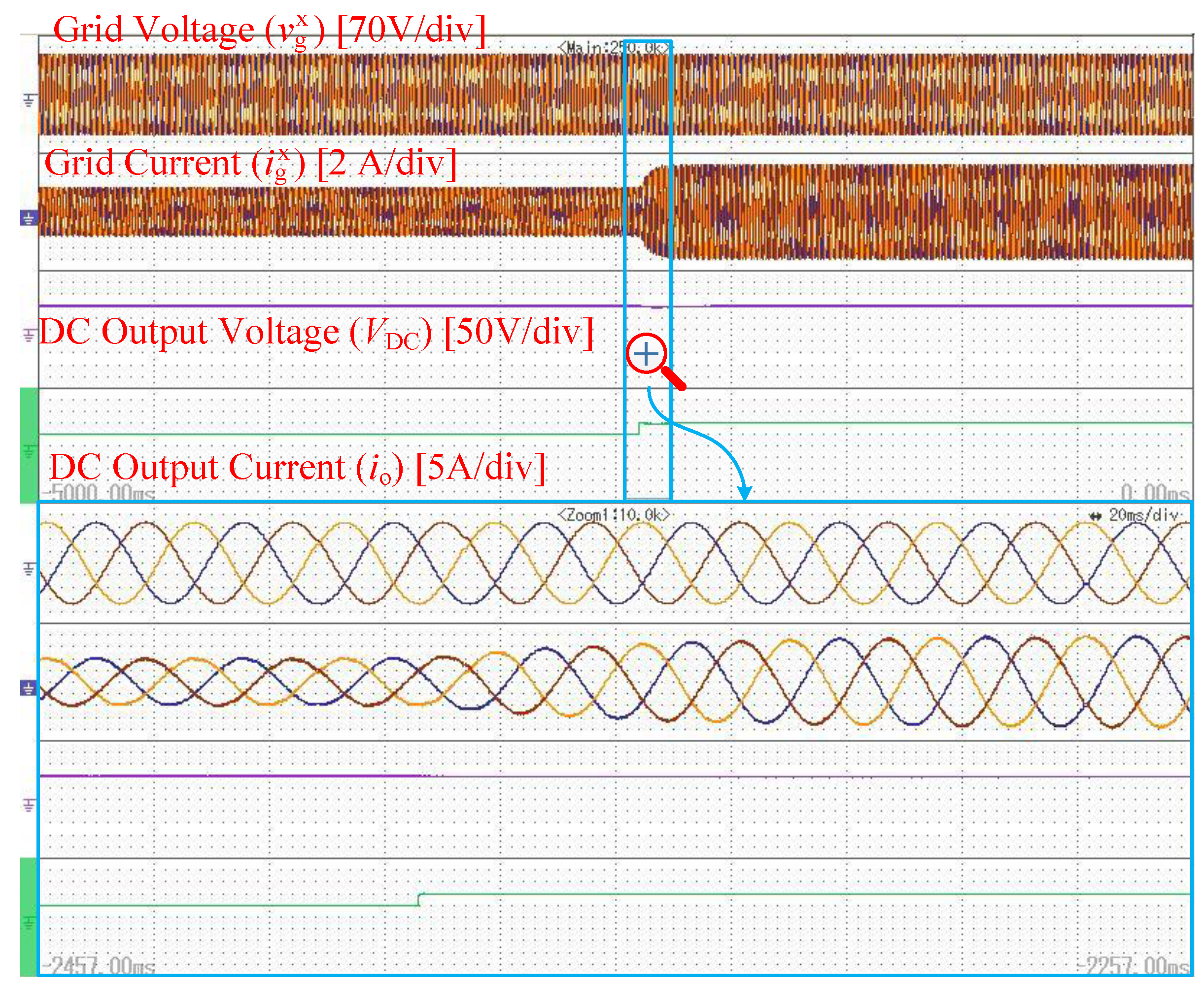
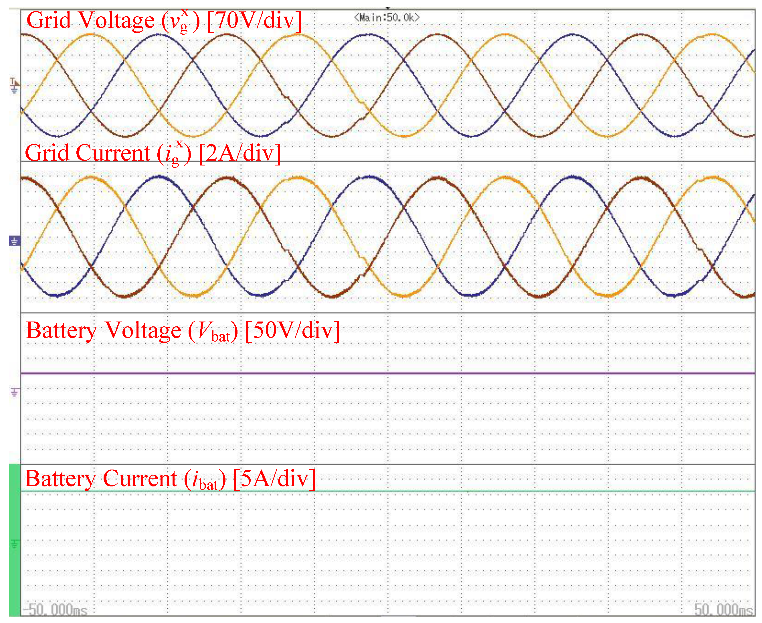
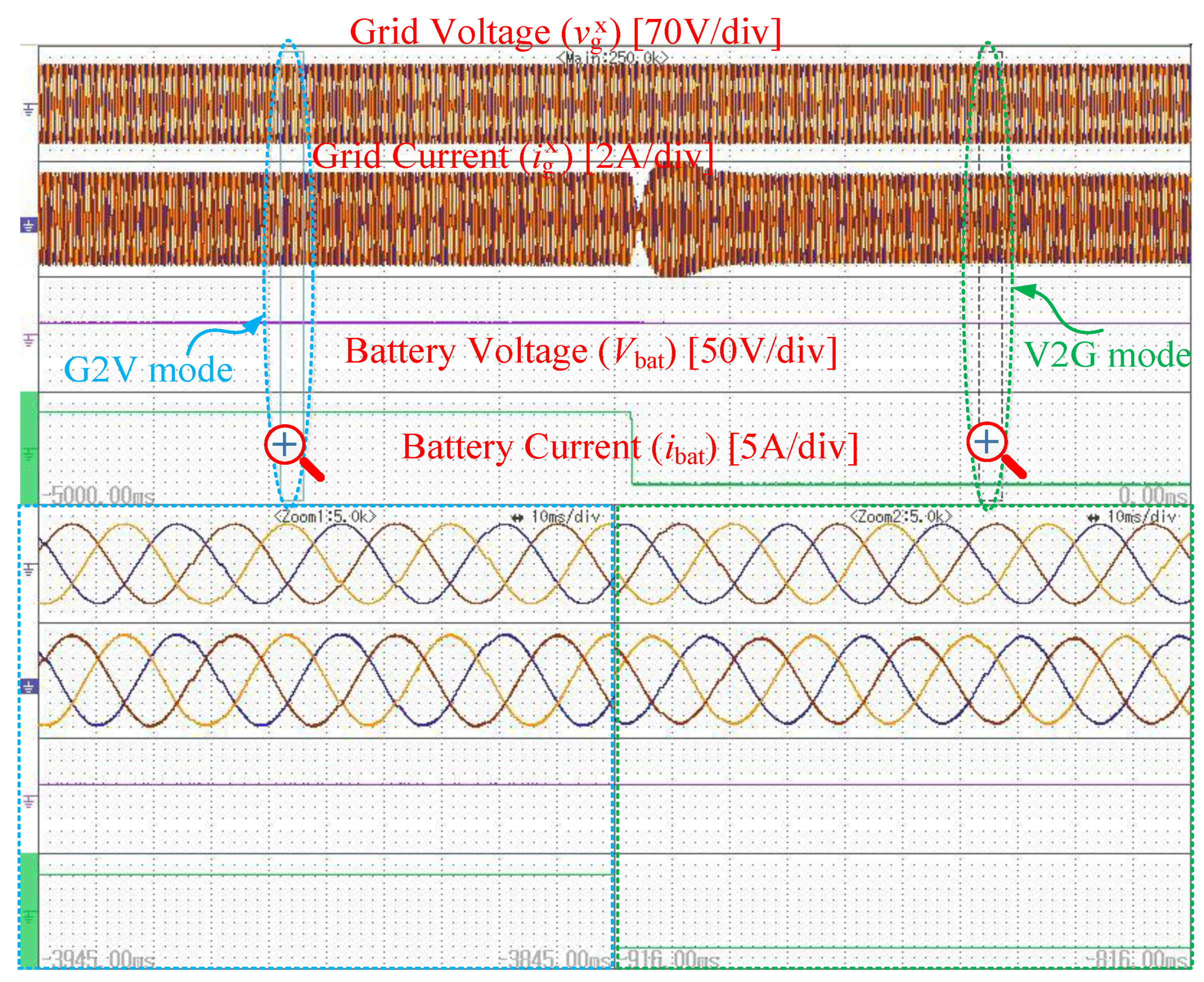
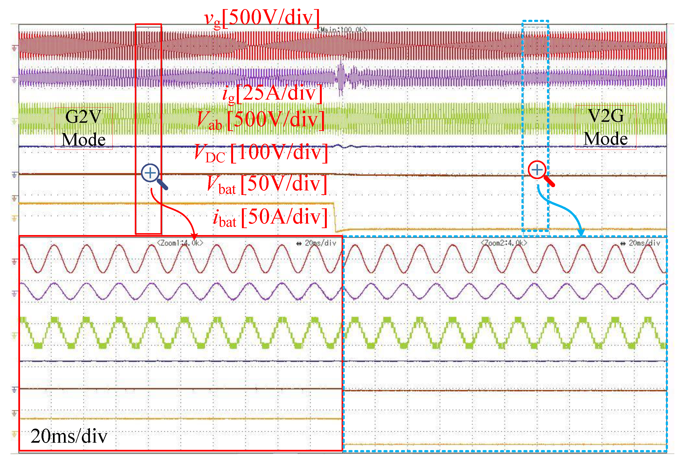
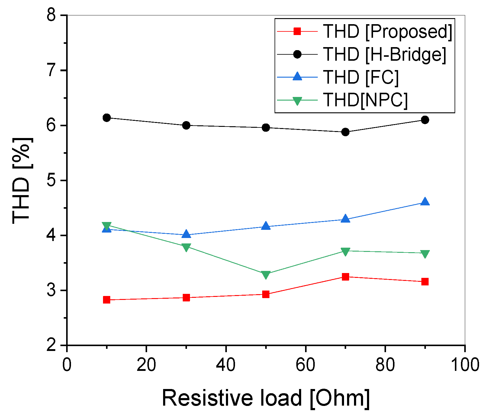
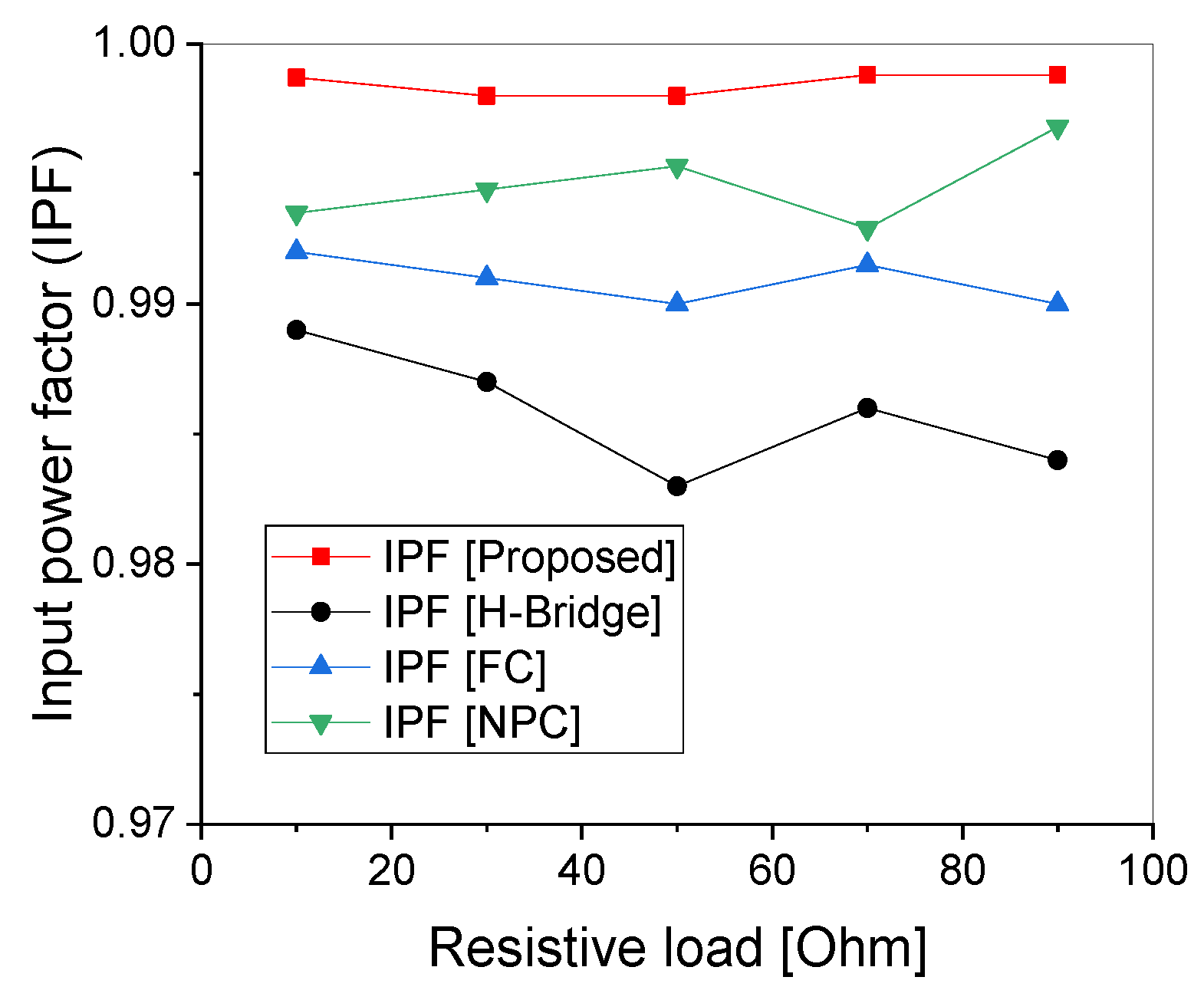
5. Experimental Results
6. Conclusions
- It synthesizes input into four levels as a pole voltage and seven levels as a line voltage, enhancing the waveform’s harmonic profile.
- It has a wide output voltage range and can work in buck and boost mode, making it suitable for many applications.
- The proposed rectifier is suitable for EV battery charging due to its buck mode of operation.
- It operates in continuous conduction mode (CCM), which eliminates the need for large filters.
- It has an inbuilt self-voltage balancing capability that does not require extra circuitry.
- It is capable of bidirectional power flow.
- It achieves an efficiency of 95.46%, low THD and high IPF compared to the conventional multilevel rectifier.
Author Contributions
Funding
Institutional Review Board Statement
Informed Consent Statement
Data Availability Statement
Acknowledgments
Conflicts of Interest
References
- Chan, C.C. The State of the Art of Electric and Hybrid Vehicles. Proc. IEEE 2002, 90, 247–275. [Google Scholar] [CrossRef] [Green Version]
- Yilmaz, M.; Krein, P.T. Review of Battery Charger Topologies, Charging Power Levels, and Infrastructure for Plug-in Electric and Hybrid Vehicles. IEEE Trans. Power Electron. 2013, 28, 2151–2169. [Google Scholar] [CrossRef]
- Su, W.; Eichi, H.; Zeng, W.; Chow, M.Y. A Survey on the Electrification of Transportation in a Smart Grid Environment. IEEE Trans. Ind. Inform. 2012, 8, 1–10. [Google Scholar] [CrossRef]
- Kisacikoglu, M.C.; Kesler, M.; Tolbert, L.M. Single-Phase on-Board Bidirectional PEV Charger for V2G Reactive Power Operation. IEEE Trans. Smart Grid 2015, 6, 767–775. [Google Scholar] [CrossRef]
- Kumar, V.; Yi, K. Single-Phase, Bidirectional, 7.7 KW Totem Pole On-Board Charging/Discharging Infrastructure. Appl. Sci. 2022, 12, 2236. [Google Scholar] [CrossRef]
- Kisacikoglu, M.C.; Ozpineci, B.; Tolbert, L.M. EV/PHEV Bidirectional Charger Assessment for V2G Reactive Power Operation. IEEE Trans. Power Electron. 2013, 28, 5717–5727. [Google Scholar] [CrossRef]
- Madawala, U.K.; Thrimawithana, D.J. A Bidirectional Inductive Power Interface for Electric Vehicles in V2G Systems. IEEE Trans. Ind. Electron. 2011, 58, 4789–4796. [Google Scholar] [CrossRef]
- Tariq, A. A Modified Battery Charger with Power Factor Correction for Plug-In Electrical Vehicles. In Proceedings of the The 1st International Conference on Energy, Power and Environment, Basel, Switzerland, 9 March 2022; p. 103. [Google Scholar]
- Rothmund, D.; Guillod, T.; Bortis, D.; Kolar, J.W. 99.1% Efficient 10 KV SiC-Based Medium-Voltage ZVS Bidirectional Single-Phase PFC AC/DC Stage. IEEE J. Emerg. Sel. Top. Power Electron. 2019, 7, 779–797. [Google Scholar] [CrossRef]
- Haller, S.; Alam, M.F.; Bertilsson, K. Reconfigurable Battery for Charging 48 V EVs in High-Voltage Infrastructure. Electronics 2022, 11, 353. [Google Scholar] [CrossRef]
- Lee, J.S.; Choi, U.M.; Lee, K.B. Comparison of Tolerance Controls for Open-Switch Fault in a Grid-Connected T-Type Rectifier. IEEE Trans. Power Electron. 2015, 30, 5810–5820. [Google Scholar] [CrossRef]
- Ramakrishnan, H.; Rangaraju, J. Power Topology Considerations for Electric Vehicle Charging Stations; Texas Instruments: Dallas, TX, USA, 2020. [Google Scholar]
- Lee, S.S. Single-Stage Switched-Capacitor Module (S3CM) Topology for Cascaded Multilevel Inverter. IEEE Trans. Power Electron. 2018, 33, 8204–8207. [Google Scholar] [CrossRef] [Green Version]
- Soeiro, T.B.; Friedli, T.; Kolar, J.W. Swiss Rectifier—A Novel Three-Phase Buck-Type PFC Topology for Electric Vehicle Battery Charging. In Proceedings of the 2012 Twenty-Seventh Annual IEEE Applied Power Electronics Conference and Exposition (APEC), Orlando, FL, USA, 5–9 February 2012; pp. 2617–2624. [Google Scholar]
- Xie, X.; Zhao, C.; Zheng, L.; Liu, S. An Improved Buck PFC Converter with High Power Factor. IEEE Trans. Power Electron. 2013, 28, 2277–2284. [Google Scholar] [CrossRef]
- Choi, H. Interleaved Boundary Conduction Mode (BCM) Buck Power Factor Correction (PFC) Converter. IEEE Trans. Power Electron. 2013, 28, 2629–2634. [Google Scholar] [CrossRef]
- Wu, X.; Yang, J.; Zhang, J.; Qian, Z. Variable On-Time (VOT)-Controlled Critical Conduction Mode Buck PFC Converter for High-Input AC/DC HB-LED Lighting Applications. IEEE Trans. Power Electron. 2012, 27, 4530–4539. [Google Scholar] [CrossRef]
- Teixeira, C.A.; Holmes, D.G.; McGrath, B.P. Single-Phase Semi-Bridge Five-Level Flying-Capacitor Rectifier. Proc. IEEE Trans. Ind. Appl. 2013, 49, 2158–2166. [Google Scholar] [CrossRef]
- Zhou, D.; Jiang, C.; Quan, Z.; Li, Y. Vector Shifted Model Predictive Power Control of Three-Level Neutral-Point-Clamped Rectifiers. IEEE Trans. Ind. Electron. 2020, 67, 7157–7166. [Google Scholar] [CrossRef]
- Khazraei, M.; Sepahvand, H.; Ferdowsi, M.; Corzine, K.A. Hysteresis-Based Control of a Single-Phase Multilevel Flying Capacitor Active Rectifier. IEEE Trans. Power Electron. 2013, 28, 154–164. [Google Scholar] [CrossRef]
- Najjar, M.; Kouchaki, A.; Nielsen, J.; Dan Lazar, R.; Nymand, M. Design Procedure and Efficiency Analysis of a 99.3% Efficient 10 KW Three-Phase Three-Level Hybrid GaN/Si Active Neutral Point Clamped Converter. IEEE Trans. Power Electron. 2022, 37, 6698–6710. [Google Scholar] [CrossRef]
- Syu, Y.L.; Liao, Z.; Fu, N.T.; Liu, Y.C.; Chiu, H.J.; Pilawa-Podgurski, R.C.N. Design and Control of a High Power Density Three-Phase Flying Capacitor Multilevel Power Factor Correction Rectifier. In Proceedings of the Conference Proceedings—IEEE Applied Power Electronics Conference and Exposition (APEC), Phoenix, AZ, USA, 14–17 June 2021; pp. 613–618. [Google Scholar]
- Cortez, D.F.; Barbi, I. A Three-Phase Multilevel Hybrid Switched-Capacitor PWM PFC Rectifier for High-Voltage-Gain Applications. IEEE Trans. Power Electron. 2016, 31, 3495–3505. [Google Scholar] [CrossRef]
- Mukherjee, D.; Kastha, D. A Reduced Switch Hybrid Multilevel Unidirectional Rectifier. IEEE Trans. Power Electron. 2019, 34, 2070–2081. [Google Scholar] [CrossRef]
- Itoh, J.I.; Noge, Y.; Adachi, T. A Novel Five-Level Three-Phase PWM Rectifier with Reduced Switch Count. IEEE Trans. Power Electron. 2011, 26, 2221–2228. [Google Scholar] [CrossRef]
- Abarzadeh, M.; Khan, W.A.; Weise, N.; Al-Haddad, K.; El-Refaie, A.M. A New Configuration of Paralleled Modular ANPC Multilevel Converter Controlled by an Improved Modulation Method for 1 MHz, 1 MW EV Charger. IEEE Trans. Ind. Appl. 2021, 57, 3164–3178. [Google Scholar] [CrossRef]
- Yalla, N.; Babu, N.A.; Agarwal, P. A New Three-Phase Multipoint Clamped 5L-HPFC with Reduced PSD Count and Switch Stress. IEEE Trans. Ind. Electron. 2020, 67, 2532–2543. [Google Scholar] [CrossRef]
- Dell’Aquila, A.; Liserre, M.; Monopoli, V.G.; Rotondo, P. Overview of PI-Based Solutions for the Control of DC Buses of a Single-Phase H-Bridge Multilevel Active Rectifier. IEEE Trans. Ind. Appl. 2008, 44, 857–866. [Google Scholar] [CrossRef]
- Vahedi, H.; Al-Haddad, K. A Novel Multilevel Multioutput Bidirectional Active Buck Pfc Rectifier. IEEE Trans. Ind. Electron. 2016, 63, 5442–5450. [Google Scholar] [CrossRef]
- Babaie, M.; Al-Haddad, K. A Novel Single-Phase Triple-Output Active Buck Rectifier Using Nine-Level Packed E-Cell Converter. In Proceedings of the SEST 2021—4th International Conference on Smart Energy Systems and Technologies, Vaasa, Finland, 6–8 September 2021. [Google Scholar]
- Kazmierkowski, M.P.; Malesani, L. Current Control Techniques for Three-Phase Voltage-Source Pwm Converters: A Survey. IEEE Trans. Ind. Electron. 1998, 45, 691–703. [Google Scholar] [CrossRef]
- Carrara, G.; Gardella, S.; Marchesoni, M.; Salutari, R.; Sciutto, G. A New Multilevel PWM Method: A Theoretical Analysis. IEEE Trans. Power Electron. 1992, 7, 497–505. [Google Scholar] [CrossRef]
- Zmood, D.N.; Holmes, D.G. Stationary Frame Current Regulation of PWM Inverters with Zero Steady State Error. In Proceedings of the PESC Record—IEEE Annual Power Electronics Specialists Conference, Charleston, SC, USA, 1 July 1999; Volume 2, pp. 1185–1190. [Google Scholar]


| Power Level | Charger Type | Input Supply | Supply Interface | Power Level |
|---|---|---|---|---|
| Level-1 | On-board single-phase | 120 V RMS | Convenience outlet | 1.4 kW (12 A) 2 kW (20 A) |
| Level-2 | On-board Single/three-phase | 230 V RMS | Dedicated charging point | 8 kW (32 A) 19.2 kW (80 A) |
| Level-3 | Off-board three-phase | 415 V RMS | Dedicated charging station | 50 kW–200 kW |
| States | Switches | Capacitors | Pole Voltage | |||||
|---|---|---|---|---|---|---|---|---|
| Sx1 | Sx3 | Sx5 | Sx6 | Cx1 | Cx2 | Co | Vxn | |
| 1 | 0 | 1 | 1 | 1 | Charging | Charging | Discharging | 0 |
| 2 | 1 | 1 | 1 | 1 | Discharging | Discharging | Charging | +VDC |
| 3 | 1 | 0 | 0 | 1 | Charging | Neutral | Charging | +2 VDC |
| 4 | 1 | 0 | 0 | 0 | Charging | Charging | Charging | +3 VDC |
| Parameters | Boost Topologies | Buck Topologies | |||||
|---|---|---|---|---|---|---|---|
| H-Bridge [9] | NPC [19] | FC [20] | CHB [28] | [29] | [30] | Proposed | |
| NL | 3 | 5 | 5 | 5 | 5 | 9 | 7 |
| Ns | 4 | 8 | 8 | 8 | 6 | 8 | 16 |
| ND | 0 | 4 | 0 | 0 | 0 | 0 | 0 |
| NC | 1 | 2 | 3 | 2 | 2 | 3 | 5 |
| PIV | 1 | 1 | 1 | 1 | 2 | 4 | 1 |
| Gain (1/β) | 1 | 1 | 1 | 0.5 | 0.5 | 0.25 | 1/3 |
| NVS | 2 | 2 | 2 | 3 | 3 | 4 | 2 |
| NCS | 1 | 1 | 1 | 1 | 1 | 4 | 1 |
| References | NL | NS | ND | NC | Gain (1/β) | Bidirectional Capability | Output Voltage |
|---|---|---|---|---|---|---|---|
| [21] | 5 | 18 | 0 | 2 | 1 | Yes | Boost |
| [11] | 5 | 12 | 0 | 2 | 2 | Yes | Boost |
| [22] | 5 | 12 | 0 | 4 | 1 | Yes | Boost |
| [23] | 5 | 6 | 24 | 12 | 1 | No | Boost |
| [24] | 9 | 12 | 24 | 8 | 1 | No | Boost |
| [25] | 9 | 12 | 12 | 8 | 1 | No | Boost |
| [27] | 9 | 24 | 0 | 4 | 1 | Yes | Boost |
| [26] | 13 | 54 | 0 | 2 | 1 | Yes | Boost |
| Proposed | 7 | 24 | 0 | 7 | 1/3 | Yes | Buck |
| Parameters | Value | Unit |
|---|---|---|
| Input voltage | 170 V for three-phase and 230 V for single-phase | V (RMS) |
| Input grid frequency | 50 | Hz |
| Filter inductor | 4 | mH |
| Capacitors (ALF80C162DF200) | 1600 | μF |
| Switching frequency | 10 | kHz |
| DC load | 10, 20, 30 | Ω |
| Output DC voltage | 100 V for three-phase and 120 V for single-phase | V |
| Battery | 48 V, 30 AH Lithium-ion ferrous phosphate | |
| Semiconductor switches | SiHG47N6 | |
| Gate driver IC | Si82071AB-IS | |
| Hall effect voltage sensor | LEM LV25-P | |
| Current sensor | HE025T01 | |
Publisher’s Note: MDPI stays neutral with regard to jurisdictional claims in published maps and institutional affiliations. |
© 2022 by the authors. Licensee MDPI, Basel, Switzerland. This article is an open access article distributed under the terms and conditions of the Creative Commons Attribution (CC BY) license (https://creativecommons.org/licenses/by/4.0/).
Share and Cite
Jain, A.; Gupta, K.K.; Jain, S.K.; Bhatnagar, P.; Vahedi, H. A V2G Enabled Bidirectional Single/Three-Phase EV Charging Interface Using Modular Multilevel Buck PFC Rectifier. Electronics 2022, 11, 1891. https://doi.org/10.3390/electronics11121891
Jain A, Gupta KK, Jain SK, Bhatnagar P, Vahedi H. A V2G Enabled Bidirectional Single/Three-Phase EV Charging Interface Using Modular Multilevel Buck PFC Rectifier. Electronics. 2022; 11(12):1891. https://doi.org/10.3390/electronics11121891
Chicago/Turabian StyleJain, Anekant, Krishna Kumar Gupta, Sanjay K. Jain, Pallavee Bhatnagar, and Hani Vahedi. 2022. "A V2G Enabled Bidirectional Single/Three-Phase EV Charging Interface Using Modular Multilevel Buck PFC Rectifier" Electronics 11, no. 12: 1891. https://doi.org/10.3390/electronics11121891
APA StyleJain, A., Gupta, K. K., Jain, S. K., Bhatnagar, P., & Vahedi, H. (2022). A V2G Enabled Bidirectional Single/Three-Phase EV Charging Interface Using Modular Multilevel Buck PFC Rectifier. Electronics, 11(12), 1891. https://doi.org/10.3390/electronics11121891