Abstract
In this article, a dual-loop dual-output frequency synthesizer designed for IEEE802.11aj (45 GHz) standard is presented. In order to support the super-heterodyne transceiver, the Loop1 output frequency is fixed for easy design of high-performance IF transceiver and filter, and the Loop2 output frequency varies for the channel selection according to the IEEE802.11aj (45 GHz) standard. The power hungry high-speed prescaler (or multi-modulus-divider) is replaced with a mixer in Loop2, thus the in-band phase noise and DC power consumption can be improved. The dual-loop dual-output synthesizer is fabricated in 0.13 µm SiGe BiCMOS technology, occupies an area of 2.7 mm × 2.4 mm, and consumes 610 mW DC power. Measured results show the phase noise of the frequency synthesizer are −79.3 dBc/Hz@10 kHz and −129.1 dBc/Hz@10 MHz at 12.96 GHz for Output1 and −76.6 dBc/Hz@10 kHz and −117.2 dBc/Hz@10 MHz at 32.535 GHz for Output2. The low-reference spur of −69.2 dBc and low-power level spurious tones at the outputs are observed during the measurement. To the best of our knowledge, this work is the first reported dual-loop dual-output synthesizer designed for IEEE802.11aj (45 GHz) standard.
1. Introduction
Recently, high-data-rate communication systems with increasing bandwidth requirements have drawn much attention. The millimeter-wave frequency band with rich spectrum resources is well-matched for massive data-driven communications, such as 5G, wireless high-definition video streaming, and future ultra-high-speed wireless communication. Millimeter-wave systems, in 28/39 GHz band for 5G new radio standard and in 60 GHz bands for IEEE802.11ad/WiGig standard, have been developed for the increasing data-rate demands [1,2,3,4,5,6].
In Q-band, IEEE 802.11aj (45 GHz) standard was approved in 2018 as a IEEE802.11 family member for high-data-rate wireless personal area networks and portable devices. These devices define 10 channels with a channel bandwidth of 540 MHz or 5 channels of 1080 MHz, as shown in Figure 1, with up to 15 Gb/s data rate [7,8]. Although there are many reported synthesizer studies [9,10,11,12,13,14,15], very few synthesizer studies have been reported for the IEEE802.11aj (45 GHz) standard [16]. For the millimeter-wave transceiver design, super-heterodyne system is preferred for high-dynamic range, alleviated LO leakage, and DC-offset issues, where two or more LO frequencies (denoted as LO1, LO2, etc.) are needed in the system. To simplify the synthesizer design, sliding-IF transceiver topology is often used [2,5,6], where the LO1 frequency is harmonic-related to the LO2, so one single-loop frequency synthesizer can support the transceiver application, as shown in Figure 2a. However, in sliding-IF topology, both LO1 and LO2 are variable for selecting different channels, which add complexity in wide-band IF transceiver and filter design. On the contrary, for super-heterodyne topology with dual-loop LO synthesizer, LO1 frequency can be fixed for high-performance IF transceiver and band-pass filter design, while LO2 frequency is variable for channel selection, as shown in Figure 2b. Moreover, since LO1 and LO2 are generated by independent phase locked loops synchronized with a reference source, the overall phase noise performance can be improved, with the price of more chip area and DC power consumption.
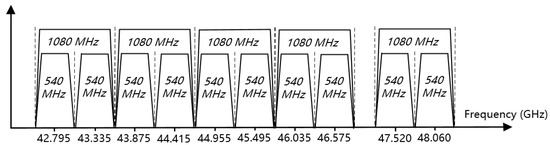
Figure 1.
Channel allocation for IEEE802.11aj (45 GHz) standard.
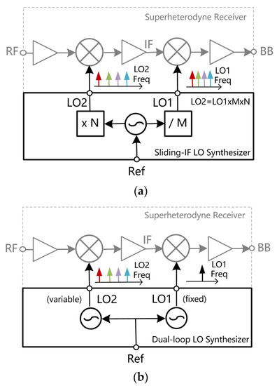
Figure 2.
Schematic of the super-heterodyne receiver with (a) the sliding-IF LO synthesizer; (b) the proposed dual-loop LO synthesizer.
In this article, the design of the dual-loop dual-output frequency synthesizer for the IEEE802.11aj (45 GHz) standard is presented. Thanks to the dual-loop topology, the frequency of Loop1 is fixed for easy design of high-performance IF transceiver and filter, and the frequency of Loop2 varies for the channel selection. In addition, the power hungry high-speed prescaler or multi-modulus-divider (MMD) is replaced with a mixer in Loop2, thus in-band phase noise degeneration can be avoided, which helps to improve the integrated phase noise for high-data-rate communications. The dual-loop dual-output synthesizer is fabricated in 0.13 µm SiGe BiCMOS process. Measured results have shown the phase noise of −79.3 dBc/Hz@10 kHz and −129.1 dBc/Hz@10 MHz at 12.96 GHz for Output1 and −76.6 dBc/Hz@10 kHz and −117.2 dBc/Hz@10 MHz at 32.535 GHz for Output2. Low-level reference spurs and spurious tones are also obtained at the outputs. In Section 2, the proposed dual-loop dual-output frequency synthesizer is designed and implemented. In Section 3, measured results of the dual-output synthesizer are provided in detail, and the conclusion is presented in Section 4.
2. Design and Implementation of the Dual-Loop Dual-Output Frequency Synthesizer
In this article, the dual-loop dual-output frequency synthesizer is proposed for the IEEE802.11aj (45 GHz) applications, and the block diagram is shown in Figure 3. In the proposed dual-loop synthesizer, the frequency of LO1 is fixed at 12.96 GHz, and the frequency of LO2 varies between 29.835~35.1 GHz for the channel selection. In this way, the output RF carrier frequency (LO2 + LO1) is 42.795~48.06 GHz, while the image frequency (LO2-LO1) is 16.875~22.14 GHz, which is reasonably away from LO1 and LO2. If needed, a bandpass filter is easy to design to suppress unwanted signals. Thus, the frequency allocation scheme is carefully chosen to simplify IF transceiver and filter design, avoiding most spurious mixing product falling into the signal band. Meanwhile, a RF down-conversion mixer is proposed in Loop2, where the Loop1′s output (12.96 GHz signal) is also the LO signal for the mixer. In this way, power consumption can be reduced by omitting high-speed prescaler/MMD, and in-band phase noise can be improved, as well. The frequency step also can be reserved as reference frequency with the Integer-N synthesizer.
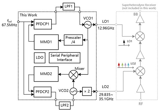
Figure 3.
Block diagram of the proposed dual-loop dual-output frequency synthesizer for IEEE802.11aj (45 GHz) standard.
Considering the frequency synthesizer implementation issues, such as the VCO phase noise performance, harmonic-frequency suppression, DC power consumption, etc., the LO1 at Ku-band (12.96 GHz) can be generated directly from VCO1, and LO2 at Ka-band from 29.835 to 35.1 GHz can be generated with VCO2, followed by a frequency doubler. In order to cover all the 540/1080 MHz channels in IEEE802.11aj (45 GHz) standard, the reference frequency of 67.5 MHz is chosen for the dual-loop Integer-N synthesizer. The VCO1, VCO2, doubler, mixer, and prescaler (in Loop1) are designed with SiGe HBT devices for low-phase noise and high-speed performance in Ku/Ka-band, which are designed and optimized with full-wave EM simulator to take into account the parasitic effects. Phase-frequency detector (PFD), charge pump (CP), and low dropout regulators (LDOs) are designed with thick gate-oxide CMOS transistors and MMD1/MMD2. Serial peripheral interface (SPI) circuits are designed with thin gate-oxide CMOS transistors, both offered with the 0.13 μm SiGe BiCMOS technology. The on-board loop filters (LPF1 and LPF2) are not integrated on the chip for flexibility and saving chip area.
2.1. Voltage Controlled Oscillator using Cap Bank and Ka-Band Doubler
Figure 4a shows the schematic of the Ku-band Colpitts VCO with 3-bit cap bank (in Loop2). The Ku-band Colpitts VCO with single varactor pair (in Loop1) uses the same topology without cap bank. The 3-bit cap bank is utilized to lower the VCO gain. The NMOS transistor is used as RF switch, which is controlled by Vsw. The capacitance in the 3-bit cap bank is binary weighted. In the Colpitts VCO, the LC tank consists of C1, C2, L2, Cvar, Le, and the 3-bit cap bank. Cvar is capacitance of the varactor, which is biased with tuning voltage, Vt. Bipolar transistor T1,2 generates the desired negative resistance to sustain oscillation. The biasing condition for T1~T4 are optimized for noise and output power. The emitter lengths for T1,2 and T3,4 are 18 µm and 10 µm, respectively. The switching signal, Vsw, is controlled by on-chip SPI. Figure 4b shows the designed Ka-band doubler, using differential Cascode core to generate second harmonic signal with sufficient gain and output power. The emitter lengths for T5,6,7,8 are all 16 µm.
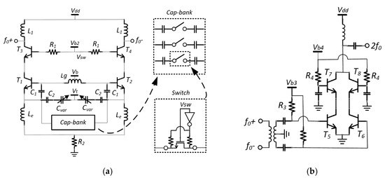
Figure 4.
Schematic of (a) the Ku-band Colpitts VCO with 3-bit cap-bank; (b) the Ka-band doubler.
2.2. High-Speed Prescaler and Double-Balanced Down-Conversion Mixer
The synthesizer Loop1 outputs a fixed frequency signal at 12.96 GHz. The corresponding prescaler consists of two current-mode logic (CML) divide-by-2 stages [17], as shown in Figure 5a, which divides the 12.96 GHz VCO output to 3.24 GHz signal. CML divider has the advantages of small area, compared to the injection-locked frequency divider. Circuit parameters are optimized for each CML stage to obtain better RF performance and lower power consumption for input signals at 12.96/6.48 GHz.
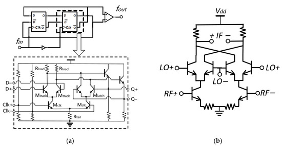
Figure 5.
Schematic of (a) the CML divide-by-2 divider; (b) the double-balanced mixer core with resistively degeneration.
The synthesizer Loop2 outputs Ku-band signal covering 14.9175~17.55 GHz. Normally, a high-speed MMD needs to be used after VCO to achieve the reference frequency step. This step introduces high-power consumption and in-band phase noise degeneration with 20lg(N), where N is the integer division ratio. In this work, instead, a down-conversion mixer is used to down-convert the Ku-band VCO signal from ~16 GHz to ~3 GHz with the 12.96 GHz LO signal from synthesizer Loop1. In this way, the power hungry high-speed prescaler or MMD can be avoided, and in-band phase noise can be improved. The double-balanced structure of down-conversion mixer reduces the LO and RF to IF port feed-through, as shown in Figure 5b. The mixer gm-stage is resistively degenerated to improve linearity. To make trade-off between the operating bandwidth and power-handling capacity, the transistor sizes are optimized for the switching quads (8 µm) and gm stage (16 µm).
2.3. Phase-Frequency Detector and Charge Pump
The PFD compares the reference signal, Fref, and the divided signal, Fdiv, and controls the CP current according to the phase and frequency difference, as shown in Figure 6a. The charge pump needs to provide matched up-and-down currents for most of the CP output voltage range. The charge-pump architecture employs dual operation amplifiers (Op-Amps), where both amplifiers utilize a high-swing topology [10]. The CP includes 3 binary weighted branches so that the current can be digitally controlled from 150 μA to 1050 μA, adapting the PLL’s loop bandwidth/settling time for various configurations. Finally, the simulated phase noise of the dual-loop dual-output synthesizer is shown in Figure 7. Figure 7a shows the simulated phase noise contributions at the Output1 from Loop1, while Figure 7b shows the simulated phase noise contributions at the Output2 from Loop2 with the frequency doubler. The loop bandwidth has been optimized to balance the in-band and out-of-band phase noise. From the phase noise contribution plot, most of them result from the integrated VCO, PFD, and CP.
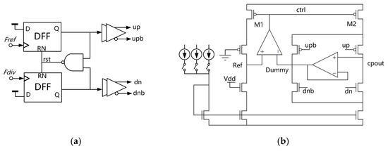
Figure 6.
Schematic of (a) the phase-frequency detector; (b) the charge pump with dual Op-Amp design for matching up-and-down currents.
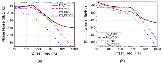
Figure 7.
Simulated phase noise contributions at (a) the Output1 from Loop1; (b) the Output2 from Loop2 with doubler.
3. Results
The proposed dual-loop dual-output frequency synthesizer is implemented using 0.13 µm SiGe BiCMOS technology. The top metal and second metal with thickness of 4 and 1.42 µm are used in the design of RF signal interconnections/passive parts, as well as the power routing, while the third metal with thickness of 0.6 µm is used as the RF/DC ground. The implemented synthesizer chip is wire-bonded to the printed circuit board (PCB), on which the PLL’s loop filters are implemented for low cost and flexibility. The output spectrum and the phase noise of the chip are measured with Keysight PXA N9030A, and R&S phase noise analyzer FSWP, which also provides the supply voltage to the low noise LDOs on PCB board, distributing the required voltages to each core circuit. The total DC power consumption is 610 mW for the dual-loop synthesizer chip. Figure 8 shows the measurement setup environment and the photograph of the wire-bonded dual-loop dual-output synthesizer. The chip size including all pads is 2.7 mm × 2.4 mm.


Figure 8.
(a) Measurement setup environment for the output spectrum and phase noise of the dual-loop dual-output synthesizer chip; (b) photograph of the wire-bonded dual-loop dual-output frequency synthesizer chip; (c) function module blocks in the chip.
Figure 9a shows the measured output frequency of the Colpitts VCO1 in Loop1, which is from 12.28 to 13.25 GHz. Figure 9b shows the measured phase noise for VCO1 at 1 MHz offset, from −112 to −116 dBc/Hz. Thanks to the high-Q varactor provided by the process, the VCO1 shows good phase noise performance with the average VCO gain, Kvco, of 485 MHz/V for the varactor tuning voltage, Vt, from 0.2~1.6 V, where the charge pump has well-matched up/down currents to optimize the phase noise and spur performance for the frequency synthesizer.
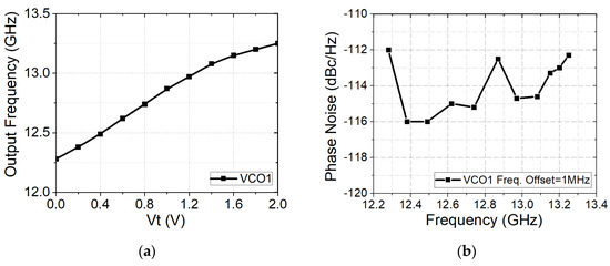
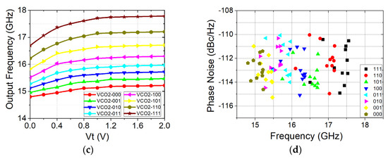
Figure 9.
Measured results for (a) the output frequency for the Colpitts VCO1 in Loop1; (b) the phase noise of the VCO1 at 1 MHz offset; (c) the output frequency for the Colpitts VCO2 with three-bit cap bank in Loop2; (d) the phase noise of the VCO2 at 1 MHz offset.
Figure 9c shows the measured output frequency of the Colpitts VCO2 with three-bit cap bank in Loop2, which is from 14.81 GHz to 17.78 GHz. The VCO2, together with the frequency doubler, can cover 29.835~35.1 GHz, which is designed to support all 540/1080 MHz channels in IEEE802.11aj (45GHz) standard. Figure 9d shows the measured phase noise for VCO2 at 1 MHz offset, from −110 dBc/Hz to −115 dBc/Hz. With the three-bit cap bank, the average Kvco is kept below 450 MHz/V for the eight sub-bands, optimizing for the phase noise performance and loop dynamics of the frequency synthesizer.
Figure 10a,b shows the measured phase noise of the dual-loop dual-output frequency synthesizer, which are −79.3 dBc/Hz@10 kHz, −88.9 dBc/Hz@100 kHz, and −129.1 dBc/Hz@10 MHz at 12.96 GHz for Output1 and −76.6 dBc/Hz@10 kHz, −80.2 dBc/Hz@100 kHz, and −117.2 dBc/Hz@10 MHz at 32.535 GHz for Output2. The two outputs of the frequency synthesizer can support the channel centered at 45.495 GHz for IEEE 802.11aj (45 GHz) in a super-heterodyne transceiver, as shown in Figure 2b. By configuring a series of division ratios (N = 29, 31, 33, …, 57, 64, 66, 68) for MMD in Loop2, all the 540/1080 MHz channels of IEEE802.11aj (45 GHz) can be supported. The loop bandwidth of the two loops is designed as ~50 kHz and ~450 kHz, respectively, to optimize the in-band/out-of-band phase noise and spur attenuation. Compared to the simulated phase noise performance in Figure 7, the measured loop bandwidths shrink 50~100 kHz for Loop1 and Loop2, possibly due to some parasitic capacitance in the loop, and the measured phase noise degrades 2~5 dB for in-band and out-of-band noise, which possibly results from the 1/f noise model for the transistor provided by the process. Compared to the Loop1, there are more spurs from Output2 of the synthesizer at 1~10 MHz offset, which is probably due to the noise coupling from the cap-bank biasing and power supply network.
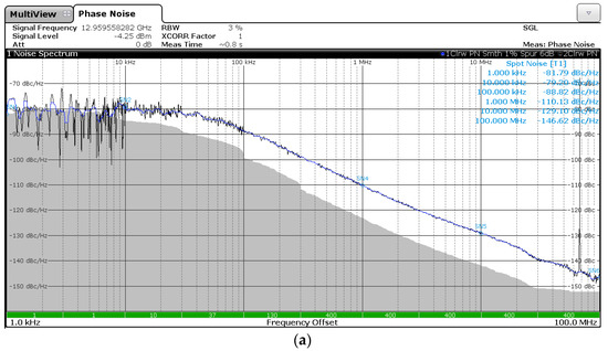
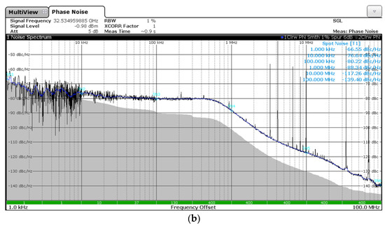
Figure 10.
Measured results for the dual-loop dual-output frequency synthesizer: (a) at 12.96 GHz for Output1; (b) at 32.535 GHz for Output2.
Figure 11a shows the measured output spectrum for the frequency synthesizer at 12.96 GHz with a span of 200 MHz, where the reference spur is below −69.2 dBc at 67.5 MHz offset. For the full span from ~DC to 50 GHz, Figure 11b shows the measured output spectrum at Output1, where the LO1 signal is with the highest power level of −4.5 dBm, and the second peak is the coupled LO2 (2 × fvco2) signal, with −17.3 dBc around ~32 GHz. Although the signal at fvco2 is close to fvco1, the power level is −39.8 dBc below. Figure 11c shows the measured output spectrum at Output2, where the LO2 (2 × fvco2) signal has the highest power level of +2 dBm, and the second peak is −19.2 dBc at fundamental frequency, fvco2. If spurious products in the mixing process are concerned, an extra band-pass filter can be used to further suppress the fvco2 signal. Table 1 compares the details of the state-of-the-art frequency synthesizers for high-speed communications. The proposed dual-loop dual-output synthesizer shows good phase noise, tuning range, and reference spurs performances. The DC power consumption is higher compared with other works in the table, mainly due to the power hungry HBT transistors in the SiGe process.
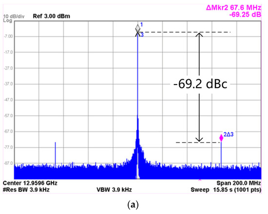
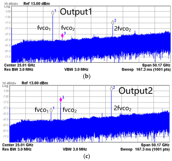
Figure 11.
Measured output spectrum for the dual-loop dual-output synthesizer: (a) reference spur level of −69.2 dBc at Output1; (b) full-span spectrum of Output1 with fvco1 as the main output frequency and 2fvco2 as the second peak; (c) full-span spectrum of Output2 with 2fvco2 as the main output frequency and fvco2 as the second peak.

Table 1.
Comparison of state-of-the-art frequency synthesizers for communications.
4. Conclusions
In this article, the development of dual-loop dual-output frequency synthesizer for IEEE802.11aj (45 GHz) is presented. By utilizing dual-loop topology, the Output1 frequency is fixed for easy design of IF filter and IF transceiver, and the Output2 frequency is variable for channel selection. In addition, the power hungry high-speed prescaler (or MMD) is replaced with a mixer in the second loop, to improve both in-band phase noise and DC power consumption. Experimental prototype has been designed and fabricated in 0.13 μm SiGe BiCMOS process. The measured phase noise are −79.3 dBc/Hz@10 kHz and −129.1 dBc/Hz@10 MHz at 12.96 GHz for Output1 and −76.6 dBc/Hz@10 kHz and −117.2 dBc/Hz@10 MHz at 32.535 GHz for Output2. The low-reference spur of −69.2 dBc and low-power level spurious tones at the outputs are also observed during the measurement. With the properly designed super-heterodyne transceiver, the proposed dual-loop dual-output frequency synthesizer is well suited for the IEEE802.11aj (45 GHz) standard.
Author Contributions
Conceptualization, Z.C.; formal analysis, Z.C. and D.H.; circuit design, Z.C.; validation, J.C. and P.Y.; review and editing, Z.C. and J.C. All authors have read and agreed to the published version of the manuscript.
Funding
This research and APC were funded by National Natural Science Foundation of China, grant number 62171128.
Institutional Review Board Statement
Not applicable.
Informed Consent Statement
Not applicable.
Data Availability Statement
Not applicable.
Conflicts of Interest
The authors declare no conflict of interest.
References
- Pang, J.; Wu, R.; Wang, Y.; Dome, M.; Kato, H.; Huang, H.; Narayanan, A.T.; Liu, H.; Liu, B.; Nakamura, T.; et al. A 28-GHz CMOS phased-array transceiver based on LO phase-shifting architecture with gain invariant phase tuning for 5G new radio. IEEE J. Solid-State Circuits 2019, 54, 1228–1242. [Google Scholar] [CrossRef]
- Fang, S.J.; Zhang, F.; Bellaouar, A.; Embabi, S. A 28 GHz Sliding-IF Receiver in 22 nm FDSOI. In Proceedings of the IEEE 45th European Solid State Circuits Conference (ESSCIRC), Cracow, Poland, 23–26 September 2019; pp. 385–388. [Google Scholar]
- Wang, Y.; Wu, R.; Pang, J.; You, D.; Fadila, A.A.; Saengchan, R.; Fu, X.; Matsumoto, D.; Nakamura, T.; Kubozoe, R.; et al. A 39-GHz 64-element phased-array transceiver with built-in phase and amplitude calibrations for large-array 5G NR in 65-nm CMOS. IEEE J. Solid-State Circuits 2020, 55, 1249–1269. [Google Scholar] [CrossRef]
- Park, H.C.; Kang, D.; Lee, S.M.; Park, B.; Kim, K.; Lee, J.; Aoki, Y.; Yoon, Y.; Lee, S.; Lee, D.; et al. 4.1 A 39 GHz-band CMOS 16-channel phased array transceiver IC with a companion dual-stream IF transceiver IC for 5G NR base-station applications. In Proceedings of the 2020 IEEE International Solid- State Circuits Conference—(ISSCC), San Francisco, CA, USA, 16–20 February 2020; pp. 76–78. [Google Scholar]
- Bozzola, S.; Guermandi, D.; Vecchi, F.; Repossi, M.; Pozzoni, M.; Mazzanti, A.; Svelto, F. A sliding IF receiver for mm-wave WLANs in 65 nm CMOS. In Proceedings of the IEEE Custom Integrated Circuits Conference, San Jose, CA, USA, 13–16 September 2009; pp. 669–672. [Google Scholar]
- Sun, Y.; Schmalz, K.; Glisic, S.; Wang, R.; Scheytt, C.J. An integrated differential 60 GHz sliding-IF receiver in SiGe BiCMOS. In Proceedings of the 3rd International Conference on Computer Research and Development, Shanghai, China, 11–13 March 2011; pp. 297–300. [Google Scholar]
- IEEE Standard 802.11aj-2018; IEEE Standard for Information Technology–Telecommunications and Information Exchange Between Systems Local and Metropolitan Area Networks–Specific Requirements Part 11: Wireless LAN Medium Access Control (MAC) and Physical Layer (PHY) Specifications Amendment 3: Enhancements for Very High Throughput to Support Chinese Millimeter Wave Frequency Bands (60 GHz and 45 GHz). Amendment to IEEE Standard 802.11-2016 as amended by IEEE Standard 802.11ai-2016 IEEE Standard 802.11ah-2016; IEEE: New York, NY, USA, 2018; pp. 1–306.
- Hong, W.; Wang, H.; Chen, J.; Zhang, N.; Zhang, Y.; Yang, G.; Yan, P.; Yu, C.; Chen, Z.; Liang, W.; et al. Recent advances in Q-LINKPAN/IEEE 802.11aj (45 GHz) millimeter wave communication technologies. In Proceedings of the 2013 Asia-Pacific Microwave Conference Proceedings (APMC), Seoul, Korea, 5–8 November 2013; pp. 227–229. [Google Scholar]
- Chen, H.-K.; Wang, T.; Lu, S.-S. A Millimeter-Wave CMOS Triple-Band Phase-Locked Loop with A Multimode LC-Based ILFD. IEEE Trans. Microw. Theory Tech. 2011, 59, 1327–1338. [Google Scholar] [CrossRef]
- Barale, F.; Sen, P.; Sarkar, S.; Pinel, S.; Laskar, J. A 60 GHz-Standard Compatible Programmable 50 GHz Phase-Locked Loop in 90 nm CMOS. IEEE Microw. Wirel. Compon. Lett. 2010, 20, 411–413. [Google Scholar] [CrossRef]
- Richard, O.; Siligaris, A.; Badets, F.; Dehos, C.; Dufis, C.; Busson, P.; Vincent, P.; Belot, D.; Urard, P. A 17.5-to-20.94 GHz and 35-to-41.88 GHz PLL in 65 nm CMOS for Wireless HD Applications. In Proceedings of the 2010 IEEE International Solid-State Circuits Conference-(ISSCC), 7–11 February 2010; pp. 252–254. [Google Scholar]
- Murphy, D.; Gu, Q.J.; Wu, Y.C.; Jian, H.Y.; Xu, Z.; Tang, A.; Wang, F.; Chang, M.C.F. A Low Phase Noise, Wideband and Compact CMOS PLL for Use in a Heterodyne 802.15.3c Transceiver. IEEE J. Solid-State Circuits 2011, 46, 1606–1617. [Google Scholar] [CrossRef]
- Park, J.; Ryu, H.; Ha, K.-W.; Kim, J.-G.; Baek, D. 76–81-GHz CMOS transmitter with a phase-locked-loopbased multichirp modulator for automotive radar. IEEE Transections Microw. Theory Tech. 2015, 63, 1399–1408. [Google Scholar] [CrossRef]
- Milosavljevic, I.M.; Glavonjic, D.P.; Krcum, D.P.; Jovanovic, S.P.; Mihajlovic, V.R.; Milovanovic, V.M. A 55–64-GHz Fully Integrated Miniaturized FMCW Radar Sensor Module for Short-Range Applications. IEEE Microw. Wirel. Compon. Lett. 2019, 29, 677–679. [Google Scholar] [CrossRef]
- Ergintav, A.; Herzel, F.; Fischer, G.; Kissinger, D. Multiplexed Twin PLLs for Wide-Band FMCW Chirp Generation in 130-nm BiCMOS. IEEE Microw. Wirel. Compon. Lett. 2019, 29, 483–485. [Google Scholar] [CrossRef]
- Chen, Z.; Wang, M.; Chen, J.-X.; Liang, W.-F.; Yan, P.-P.; Zhai, J.-F.; Hong, W. Linear CMOS LC-VCO Based on Triple-Coupled Inductors and Its Application to 40-GHz Phase-Locked Loop. IEEE Trans. Microw. Theory Tech. 2017, 65, 2977–2989. [Google Scholar] [CrossRef]
- Chen, Z.; Hou, D.; Chen, J.-X.; Yan, P.; Bao, L.; Hong, Z.; Zheng, Y. A K-Band FMCW Frequency Synthesizer Using Q-Boosted Switched Inductor VCO in SiGe BiCMOS for 77 GHz Radar Applications. Electronics 2020, 9, 1933. [Google Scholar] [CrossRef]
Publisher’s Note: MDPI stays neutral with regard to jurisdictional claims in published maps and institutional affiliations. |
© 2022 by the authors. Licensee MDPI, Basel, Switzerland. This article is an open access article distributed under the terms and conditions of the Creative Commons Attribution (CC BY) license (https://creativecommons.org/licenses/by/4.0/).