1. Introduction
With the rapid development of smart cities, cars, healthcare, industry, etc., we have experienced an increased utilization of wireless sensor networks (WSNs). The world is changing over the decades—technological development improves the quality of life. As WSN technologies evolve, the environment becomes smarter, safer, and more automated, though it requires a growing number of sensors. The widespread application of large WSNs requires more secure transmission technologies [
1]. WSN nodes are usually small battery-powered devices [
2], and security issues must be met while maintaining low power consumption and computation resource limitation considerations [
3,
4].
Several approaches ensure sufficient data transmission security in radio links between WSN nodes. Along with the use of cryptographic algorithms that require the uploading of encryption keys before transmission [
1], low-cost solutions can be used in WSN nodes that improve security at the PHY level. One of the possible solutions in this area is using chaotic oscillators to form information-carrying signals [
5]. This study aims to build a low implementation complex communication system with increased security. Utilizing the features of chaos oscillators enhances the security aspects of WSN while not noticeably increasing the complexity. With embedded chaotic oscillators, the security measures (e.g., for an eavesdropping attack) are already ensured by the inherent properties of the chaotic signals—noise-like waveforms [
6,
7], low cross-correlation between signals, high sensitivity to initial conditions, and ability of chaotic synchronization. Applying the chaotic shift keying enhances the data protection in the physical layer, increasing the security of wireless transmission at a low cost [
8]. Thus, an eavesdropping attack becomes more challenging than in the case of unsecured communication [
9,
10,
11].
The design of a communication system suitable for use in WSNs requires solving the synchronization problem. The corresponding solution is proposed in [
12], where the possibility of synchronizing two chaos oscillators was shown. A variety of chaos-based communication systems have been proposed since then, in which the used synchronization methods can be divided into two groups: coherent detection and non-coherent detection [
13,
14]. The main difference between the types of detection is the presence of a chaotic circuit at the receiver. Coherent detection requires one chaos oscillator operating in master mode at the transmitter and an identical chaos oscillator at the receiver in the slave mode to establish a chaotic synchronization.
In contrast, non-coherent detection does not require a chaotic circuit at the receiver. The coherent-detection-based systems benefit from a potential higher physical layer security, while the noncoherent-detection-based systems provide a more straightforward receiver design. The number of implemented chaos oscillators can also categorize the communication systems. Multiple chaotic signals in the transmitter allow the development of multi-carrier systems suitable for the base nodes of WSNs.
Since a low-cost approach is highly desirable for a WSN communication system, the frequency modulation (FM) systems meet this requirement. The simplicity of implementation results in these systems’ widespread use and robust applications since they do not require any unique or specialized components for the modulator.
Various research [
15,
16,
17] focused on noise immunity studies of the communication systems’ frequency-modulated differential chaos shift keying (FM-DCSK). In this modulation scheme, each transmitted symbol is represented by two sequential chaotic signal segments: the first being the reference signal and the second carrying the data. Typically, the reference signal is sent during the first half symbol period, and the data carrier signal is sent during the second half symbol period. The receiver evaluates the correlation between the reference signal and the data carrier signal using non-coherent detection. On the one hand, the FM-DCSK communication system is based on non-coherent detection, which makes such a system easier to build. On the other hand, non-coherent detection makes such a communication system less secure. The disadvantage of the FM-DCSK communication system is the reduced transmission speed and the sensitivity to noise in the transmission channel.
Another proposed system is the frequency-modulated antipodal chaos shift keying (FM-ACSK) digital communication system. The concept of the said system was proposed in [
13] along with the system’s evaluation. In this communication system, a sequence of bit shifts key a chaotic signal, and synchronization between transmitter and receiver is provided via a negative feedback loop in the receiver. The receiver uses two chaos oscillators to detect the information signal. The digital (FPGA-based) implementation of chaos oscillators leads to the transition to the periodic modes in sufficiently long time intervals due to number rounding and final accuracy of calculations [
18].
This paper introduces and studies the novel frequency-modulated chaos shift keying (FM-CSK) system for WSN applications. The proposed system employs coherent detection, a bit sequence shift keys between two chaotic signals and one chaotic signal for synchronization using the substitution method. The said system can be expanded to utilize more signals generated by the chaos oscillator, increasing the complexity. Unlike the FM-DCSK communication system, the proposed FM-CSK system increases the transmission speed. Moreover, the proposed communication system provides a higher security level because of coherent detection. Compared to the previously proposed FM-ACSK system, the FM-CSK system uses only one chaos oscillator in the receiver employing the substitution method for chaotic synchronization. The chosen oscillators are simple analog circuits. Studies [
19,
20] have shown that the analog chaos oscillator-based communication system is more energy-efficient than the FPGA-based solution.
As the FM-CSK communication system is built using analog chaos oscillators, as the first step of the study, it is essential to first explore the stability of their dynamics. The main characteristics of the chaos oscillator—the ability to synchronize and low signal cross-correlation—depend on the nominal values of individual electronic components, and the system’s synchronization relies on the similarity of chaos oscillators. Physical components have parasitic parameters and tolerances, making it necessary to perform simulation and experimental studies to determine how the chaos oscillators’ component nominal deviations impact the dynamics. It is especially relevant for reactive elements (capacitors and inductors) produced with low nominal precision, which could be critical for the FM-CSK systems’ mass-production with off-the-shelf components and system application for WSN communications. The FM-CSK system’s performance depends on the chaos oscillators’ dynamic stability, synchronization durability, and frequency domain properties of transmitted chaotic signals. Chaotic synchronization of the FM-CSK system is crucial for precise signal detection; therefore, a comprehensive analysis of synchronization has been performed in the current study.
The paper is organized as follows.
Section 2 describes the concept and operating principles of the proposed FM-CSK system.
Section 3 is devoted to studying the applied chaos oscillators’ dynamic stability and synchronization properties.
Section 4 describes FM-CSK’s performance by employing different chaos oscillators.
Section 5 concludes the work.
2. Concept of the FM-CSK Communication System
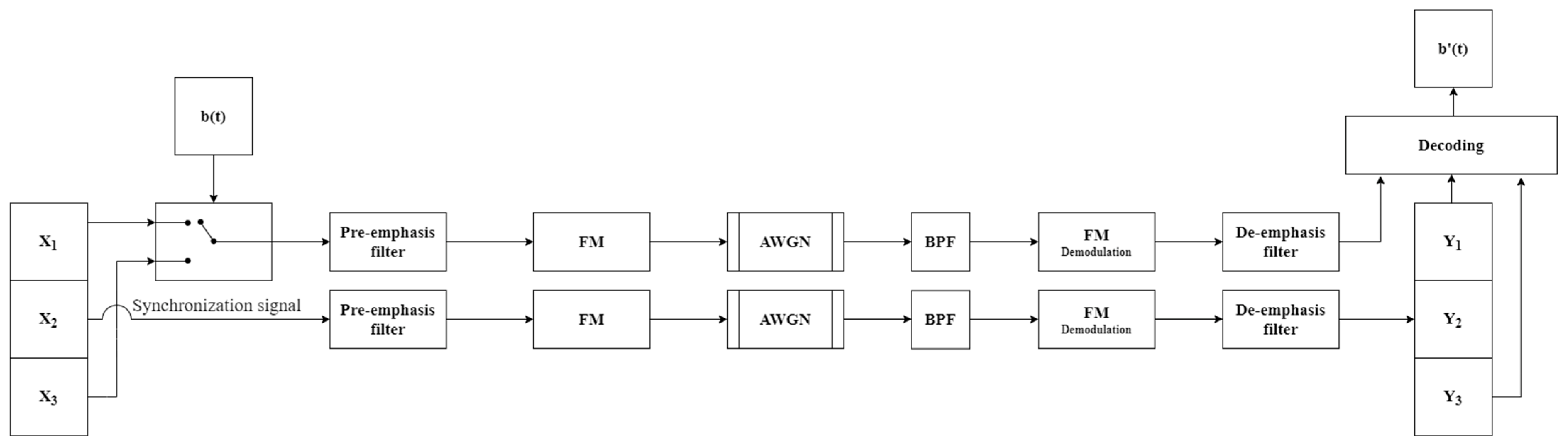
The current section presents the concept of a communication system based on frequency modulation and chaos shift keying (CSK). The block diagram of the proposed FM-CSK communication system is shown in
Figure 1. The core of the communication system is chaos oscillators working in master-slave mode. In the transmitter, the master oscillator generates three state variables (
X1,
X2,
X3); in turn, on the receiver side, the slave oscillator generates only two state variables (
Y1,
Y3) while one of the variables (
Y2) is substituted by the transmitted signal from the master oscillator (
X2). In such a scheme, the signal from the state variable (
X2) of the master circuit is used as a synchronization signal. The other state variables (
X1 and
X3) of the master circuit are used to transmit the information (
Figure 1). All state variables are chaotic signals: voltages across and currents through the circuit elements in physically implemented chaos oscillators.
The information-carrying signal is formed using a binary information-signal-controlled switch, which toggles between signals X1 and X3. Bit “1” shifts to X1 and bit “0” shifts to X3. Before an information-carrying signal is formed, X1 and X3 signals should be DC-cancelled, and their amplitudes must be matched. The DC component is suppressed in the synchronization signal as well. The formed information-carrying and synchronization signals are passed through the pre-emphasis filter. Then, both signals are used for frequency modulation and are transmitted in parallel (e.g., using different frequencies or polarization) through an additive white Gaussian noise (AWGN) channel.
In the receiver, signals are bandpass-filtered, frequency-demodulated, and passed through a de-emphasis filter. The information bits are detected by calculating the correlation coefficient between the received signal and signals
Y1 and
Y3 from the slave circuit. If
, then data bit “1” is detected, otherwise—“0”. For precise bit detection, master and slave circuits’ signals must agree. Thus, chaotic synchronization between the two chaos oscillators is crucial for correct signal detection. Therefore, the properties of chaos oscillators are examined in the next section. Moreover, a bit error ratio (BER) estimation is performed in
Section 4 to verify the obtained results and evaluate the communication system’s noise immunity.
3. Chaos Oscillators
This section introduces nonlinear dynamical systems known as chaos oscillators and describes their use in secure communications. The chaotic signal is characterized by a broad spectrum, noise-like behavior, and high sensitivity to components’ nominal values and the system’s initial conditions [
14]. These characteristics make chaos oscillators potentially suitable for use in secure communications. However, the effects of the oscillator component nominal value deviations on the dynamics and synchronization of the system should be examined in detail as critical issues for the proposed system’s practical implementation and application in WSN. This section describes the chaos oscillators used, the research methodology, and the study results.
3.1. Description of Chaos Oscillators
Chaos is a mathematical property of dynamical systems [
21]. The chaos phenomenon in oscillators can be observed in relatively simple electronic circuits exhibiting non-repetitive bounded waveforms [
22]. Minor changes in a chaotic system’s initial conditions or any external impact cause significant changes in system dynamics, which is the main reason to study chaos oscillator dynamics and synchronization stability.
Three chaos oscillators have been selected as the core elements in the FM-CSK system for the current study due to their implementation simplicity: simple two-transistor RC chaos oscillator [
23], Vilnius chaos oscillator [
24], and Chua’s chaos oscillator [
25,
26,
27]. These chaos oscillators are defined by having at least three state variable elements (e.g., capacitors and/or inductors), a nonlinear element (e.g., a transistor or a diode) to make oscillations less predictable, and an active element (e.g., an operation amplifier) to maintain oscillations. A transistor could be used both: as an active and a nonlinear element.
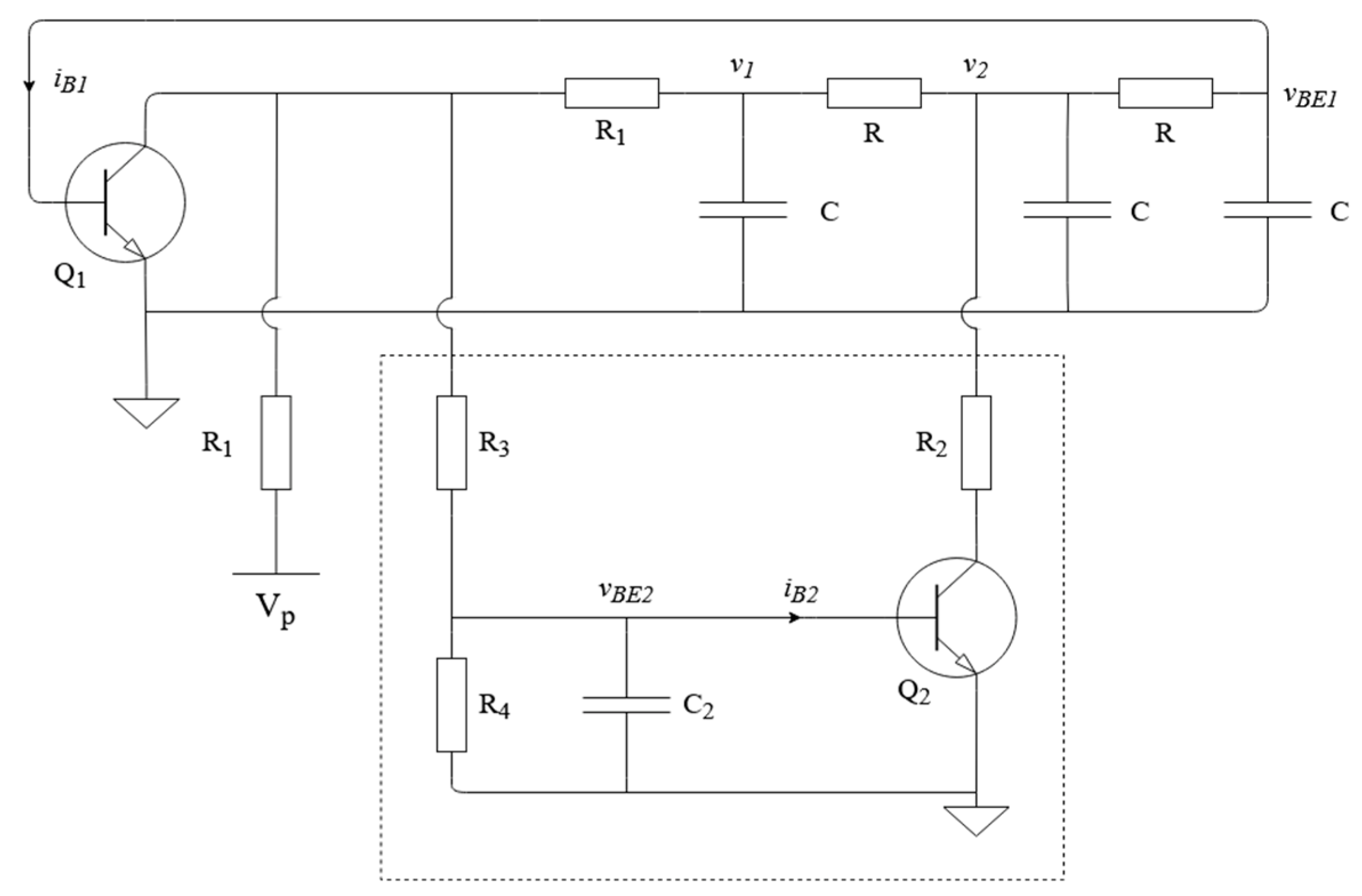
3.1.1. Two-Transistor RC Chaos Oscillator
A two-transistor RC chaos oscillator circuit is shown in
Figure 2. State variable elements are voltages across four capacitors: three
C and one
C2. Two transistors are used as nonlinear active elements. The two-transistor RC chaos oscillator circuit is constructed with a standard single-supply self-biasing RC phase shift oscillator with an added subcircuit (outlined by the dashed line box) interacting with the RC ladder [
24].
The state variable differential equations for the simple two-transistor RC chaos oscillator are [
23]:
where voltages
Vp,
v1,
v2,
vBE1, and
vBE2 are marked in
Figure 2,
iC1 and
iC2 are transistors of
Q1 and
Q2 collector currents,
iB1 and
iB2 are transistors of
Q1 and
Q2 base currents.
Transistor model currents and voltages introduce nonlinearities in the circuit. The currents
iB1,
iB2,
iC1, and
iC2 are determined by the transistor model and are functions of the collector-emitter and base-emitter voltages
vCE1,
vCE2,
vBE1, and
vBE2 [
23].
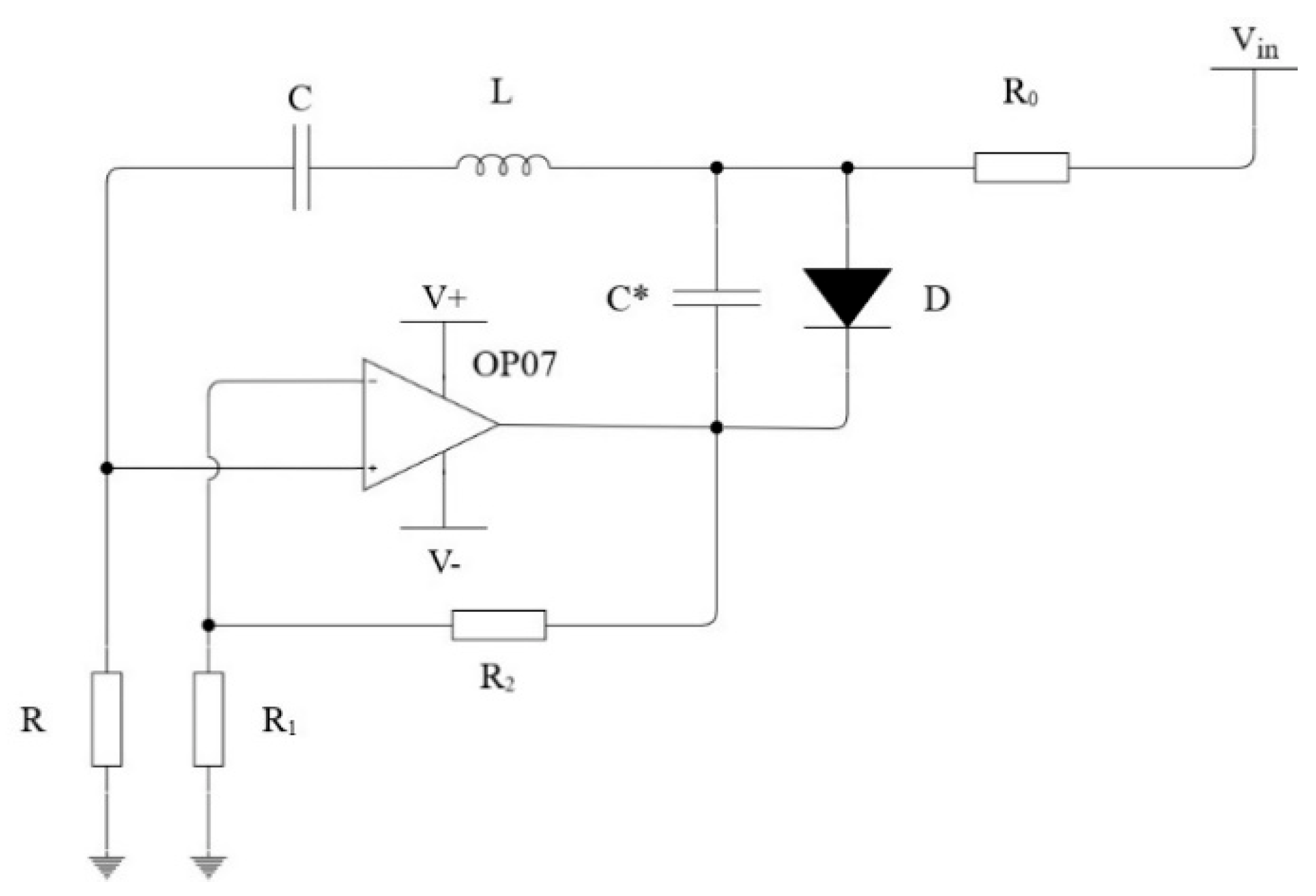
3.1.2. Vilnius Chaos Oscillator
Study [
24] describes the Vilnius chaos oscillator, also referred to as “A simple chaotic oscillator for educational purposes”. A Vilnius chaos oscillator circuit is shown in
Figure 3. The three state variables in this circuit are the voltage across capacitor
C, the current through inductor
L, and the voltage across
C*. A general-purpose silicon diode 1N4148 is used as a nonlinear element. The operational amplifier (OP AMP) OP07 is used in non-inverting mode with gain
k ≈ 1.4.
Vilnius chaos oscillator dynamics are described using the following differential equations [
24]:
where
is DC bias current,
VC is the voltage across capacitor
C,
VC* is the voltage across capacitor
C*,
IL is current through inductor
L,
k is OP AMP circuit gain,
ID is the diode’s current described by the following expression:
where
VD is the voltage across the diode (due to parallel connection
VD =
VC*),
IS is the saturation current,
VT is the thermal voltage.
Equation (8) shows that the current-voltage characteristic of the diode depends on the ambient temperature. Thus, the Vilnius chaos oscillator placed at different temperatures could generate different dynamical patterns.
3.1.3. Chua’s Chaos Oscillator
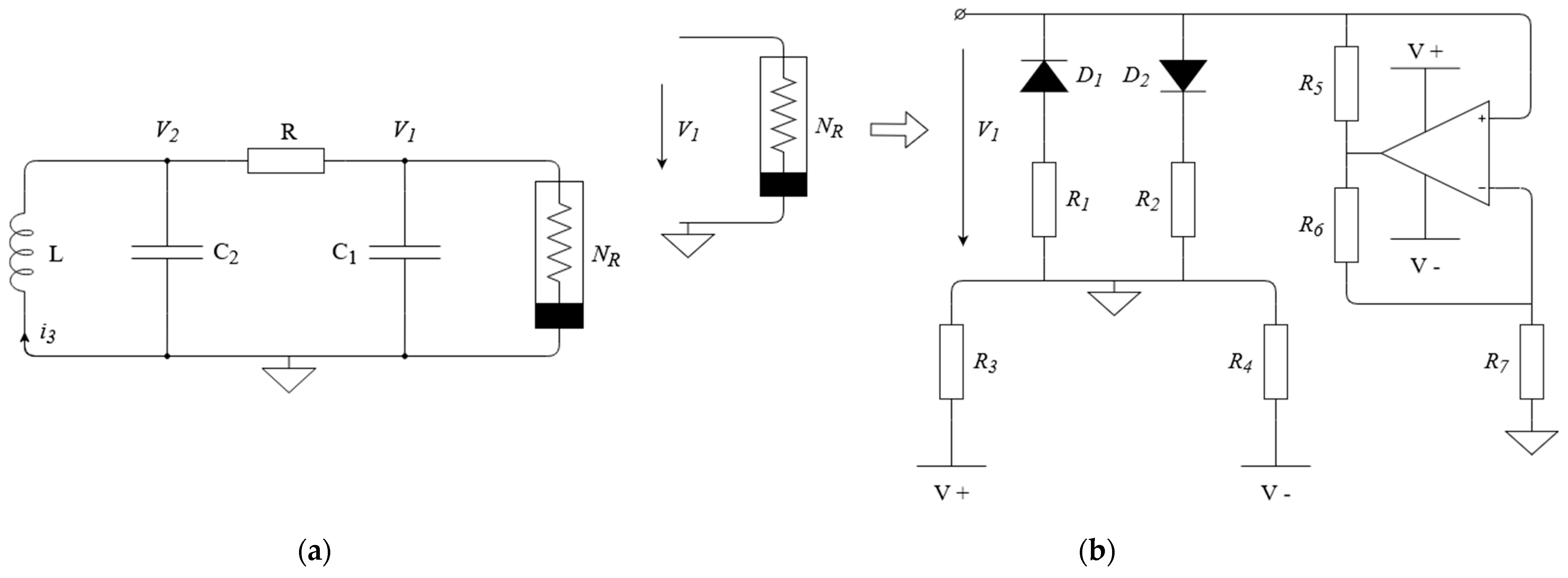
Chua’s chaos oscillator is described in [
25,
26] and shown in
Figure 4a.
This circuit has three state variables: voltages across capacitors
C1,
C2, and the current through inductor
L. The circuit diagram of Chua’s nonlinear resistor used as a nonlinear element [
25] is shown in
Figure 4b.
Chua’s chaos oscillator dynamics are described using differential equations [
25]:
where
is the resistor’s
R conductivity,
v1 is the voltage across capacitor
C1,
v2 is the voltage across capacitor
C2,
i3 is current through inductor
L. f(
v1) is a nonlinear function defined by nonlinear Chua’s resistor
NR properties.
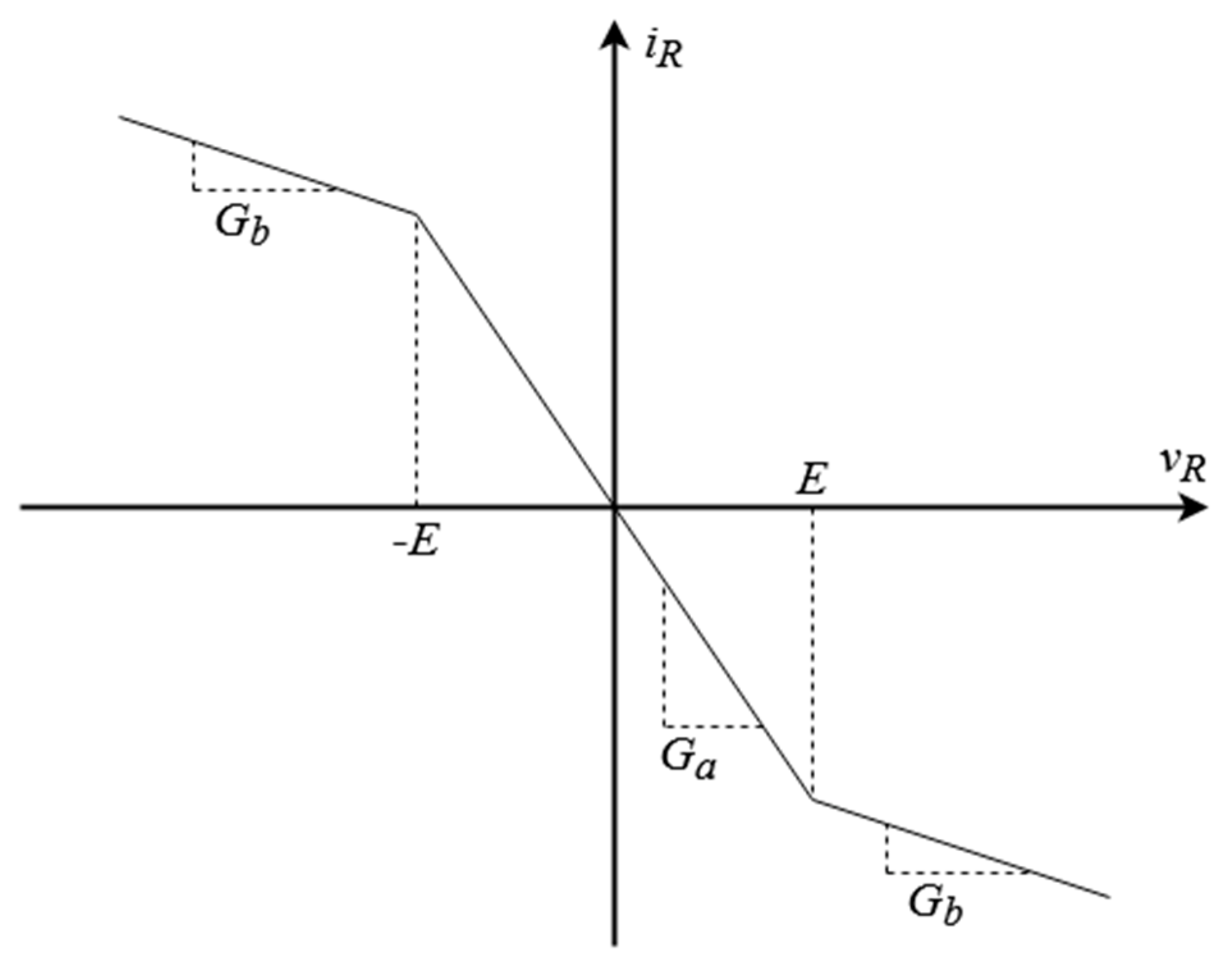
f(
v1) is a current-voltage characteristic of the
NR (
Figure 5):
where
Ga is a slope in the inner region,
Gb is a slope in the outer region,
E is the voltage across the
NR resistor. By choosing a slope in the inner region
Ga, a slope in the outer region
Gb, and the voltage
E across resistor
NR, any continuous three-segment odd-symmetric piecewise-linear current-voltage characteristic for Chua’s diode can be specified [
25].
3.2. Study on Performance of Chaos Oscillators
The first stage of this research was to study how the chaos oscillator’s initial conditions impact the oscillator’s dynamics. As mentioned before, chaos oscillator dynamics are susceptible to mismatch of initial conditions and nominal deviation of the elements. This study explores how the nominal values of reactive elements affect the chaotic system—whether it remains chaotic or shifts to periodic or quasiperiodic behavior at some nominal values.
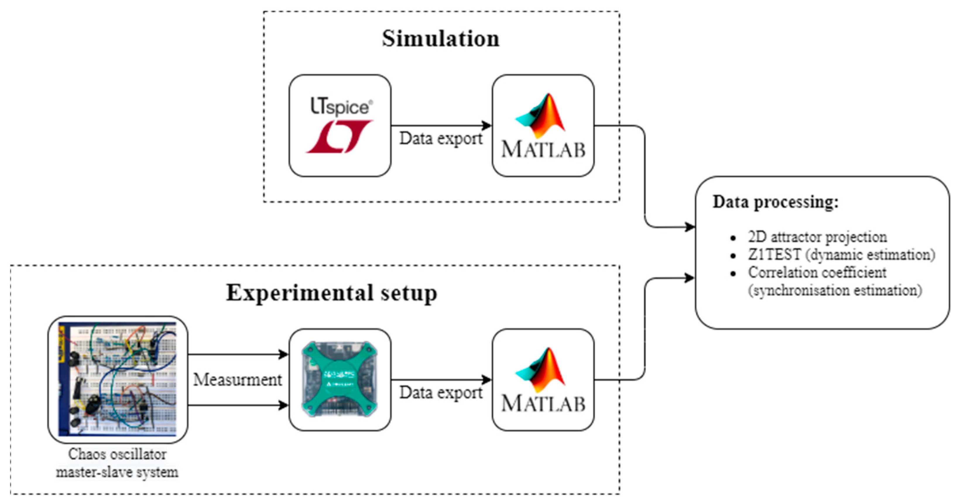
The study of chaos oscillators was performed experimentally and theoretically, employing electronic model development for a more straightforward analysis of the theoretical approach. While simulations of chaos oscillators’ models have been performed in the LTspice environment, the experimental study was performed in hardware with physical prototypes of oscillators. A simulation approach was used to test whether it could predict the hardware implementation’s behavior. The evaluation criterion of chaos oscillator design is a two-dimensional projection of the attractor: one state variable (e.g., the voltage across capacitor
C1) is displayed on the
x-axis and the other state variable (e.g., the voltage across capacitor
C2) is shown on the y-axis. The acquired two-dimensional projection’s disposition corresponds to the two-dimensional projection in the original study, demonstrating that the model was successfully implemented and ready for further examination. The Analog Discovery 2 device was used to measure voltages in hardware experiments. Data from Analog Discovery 2 and LTspice simulations were processed and analyzed in MATLAB (
Figure 6).
The second step was to study how the reactive element’s nominal deviation within ± 10% impacts the chaos system’s dynamics and synchronization and whether it is possible to predict the hardware system’s actual behavior with the simulation approach. The element’s nominal deviation reflects the most common tolerances allowed during the manufacturing of the electronic components. Due to manufacturing complexity, reactive elements (capacitors and inductors) are usually produced with lower precision than resistors. It is the reason to study reactive element influence on the chaos oscillator dynamics and synchronization. For each chaos oscillator, the nominal value of each reactive element (one by one) was changed within ± 10% from the initial value in both master and slave circuits. While one reactive element’s nominal value was altered by ± 10%, the other element values were kept constant. For hardware experiments, a capacitor array was built and measured using the Keysight Impedance analyzer E4990A (20 Hz–120 MHz). Hardware experiments were made close to simulation, considering components’ nominal deviation. System dynamics and synchronization were evaluated using the following approach in the simulations and hardware experiments. MATLAB software was used for the experimental data analysis. The mean square displacement-based 0–1 test [
28] was used to evaluate the character of the oscillator’s dynamics, while the correlation coefficient was employed to estimate the synchronization’s stability. The block diagram of the simulation and the experimental setup is presented in
Figure 6.
The correlation coefficient’s values range from 0 to 1, as the only direct signal
X1 is taken to estimate correlation with
Y1. The higher value of
indicates better synchronization. Equation (13) was used for calculating the correlation coefficient between the given signals:
where
is the correlation coefficient,
n is an array index.
3.3. Chaos Oscillator Performance Analysis
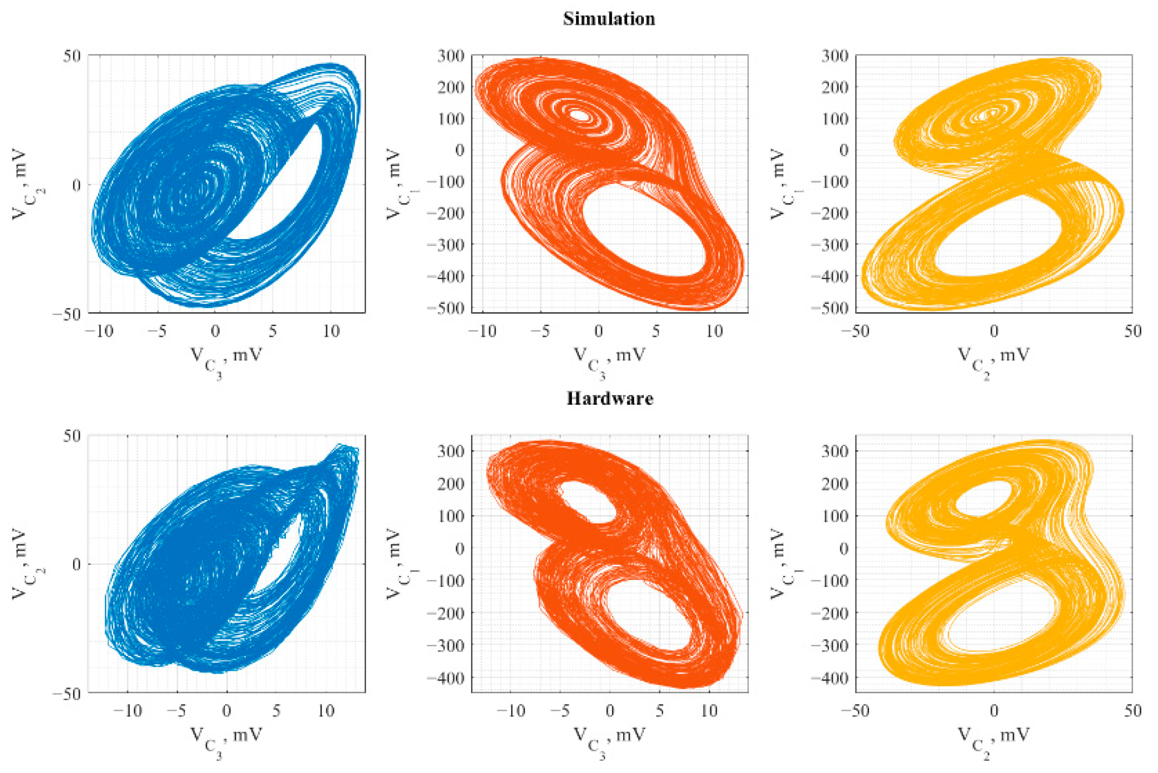
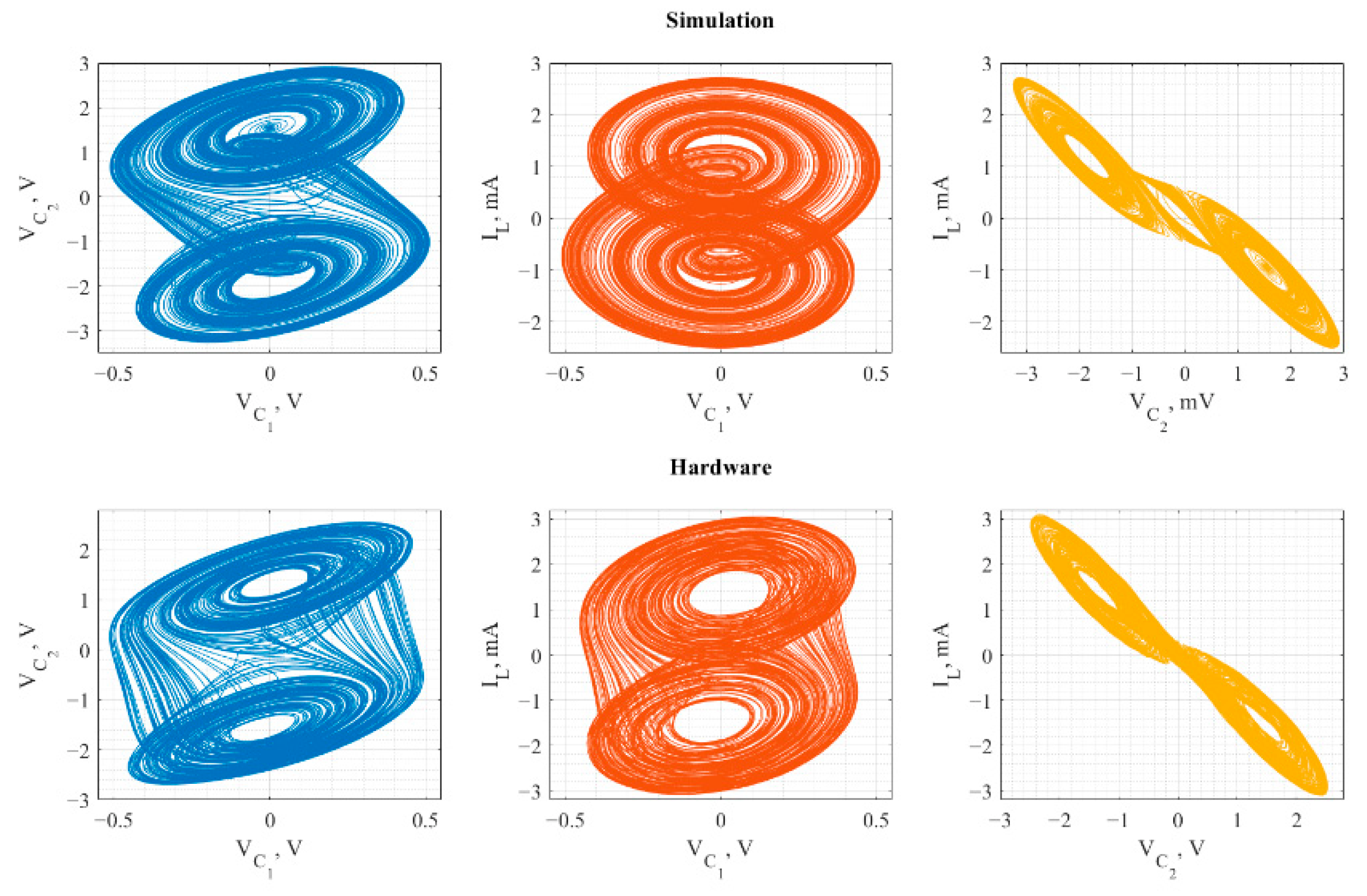
This section analyzes the results acquired in the theoretical and experimental study of the chaos oscillators’ performance. The comparative analysis examined the dynamic and synchronization stability of the developed LTspice simulation models and prototypes of the selected chaos oscillators. The first evaluation criterion compares the two-dimensional attractor projections of the oscillator obtained during the simulation and experimental measurements with the original study.
Figure 7 and
Figure 8 show the results of the dynamical behavior study implemented as a simulation model in LTspice environment and hardware circuit for RC two-transistor chaos oscillator (RC chaos oscillator) and Chua’s chaos oscillator. At the same time, the results of the experimental study on the Vilnius chaos oscillator in [
29] were used for a comparative analysis of the synchronization’s stability.
The attractor’s two-dimensional projections for the simulation model and hardware circuit were compared with the source study to evaluate the dynamic behavior of chaos oscillators. Due to the technical limitations, it was only possible to perform two simultaneous synchronous voltage measurements, and therefore, each two-dimensional attractor projection for hardware was measured separately. The behavior of the RC chaos oscillator’s two-dimensional attractor projections from simulations (
Figure 7 (top row)) and hardware experiments (
Figure 7 (bottom row)) corresponds to the source attractor projection [
23]. In turn, two-dimensional attractor projections of Chua’s chaos oscillator shown in
Figure 8 conform to the dynamic behavior of the chaos oscillator in [
26].
The key to achieving high-security communication for WSN applications is to employ chaotic synchronization between two similar chaos oscillators in the transmitter and receiver. The substitution method is used for this purpose. The signal in the slave circuit is substituted by a similar signal from the master circuit (e.g.,
C2 voltage in the master circuit is used to substitute
C2 voltage in the slave circuit). In this case, chaotic synchronization is obtained using OP-AMP in voltage follower mode [
30,
31]. When two chaos oscillators are synchronized in the master-slave system, the correlation coefficient between voltages across the same elements in the master and slave circuits approaches 1.
Simulation and hardware experimental results for two transistor RC and Chua’s chaos oscillators are presented in
Table 1, where
Z1,
Z2, and
Z3 correspond to
C1,
C2, and
C3 for the RC chaos oscillator; to
C1,
C2, and
L1 for Chua’s chaos oscillator. For Vilnius chaos, the oscillator results are presented in
Table 2. The simulation results demonstrate that the correlation coefficient value was above 0.98, while the maximal possible value for the normalized correlation coefficient is 1, which means that the slave circuit signals precisely repeat the master circuit signals. In turn, during hardware experiments, correlation coefficient values were above 0.9. Thus, it has been proved that synchronization in the master-slave system was always present in both studies. Therefore, changing the nominal value of the reactive elements within ± 10% in the slave circuit did not affect the system’s dynamics.
System dynamics evaluation using the mean square displacement-based 0–1 test showed that the slave circuit always repeats the master circuit’s behavior during studies of nominal deviation in the slave circuit. When the element nominal was changed within ± 10% in the master circuit, the system’s behavior changed rapidly. Chaos oscillator sensitivity to initial conditions (for analog circuits—nominal deviation) is the reason for rapid behavior changes. The hardware experimental results of the nominal deviation in the master circuit are close to simulation results, as depicted in
Table 1 and
Table 2, which proves the reliability of both results. This means that simulation can be used to predict the hardware experimental results.
In the simulation, Chua’s chaos oscillator had better performance—its behavior stayed chaotic while changing the reactive element nominal values in the master circuit in more than 76% of all experiments. Suppose Vilnius chaos oscillator and RC chaos oscillator simulation results are compared. In that case, RC chaos oscillator dynamics stay chaotic more often—above 75% of all experiments, but Vilnius chaos oscillator—only slightly above 56%.
Comparing performances of all chaos oscillators, the Vilnius chaos oscillator in hardware experiments was more stable than Chua’s chaos oscillator and the RC chaos oscillator. Vilnius chaos oscillator’s performance in hardware experiments stayed chaotic in at least 70% of all experiments. If hardware experimental results for the Chua’s chaos oscillator and RC chaos oscillator are compared, the dynamics of the RC chaos oscillator stayed chaotic more often. The RC chaos oscillator remained chaotic in more than 66% of all experiments, but Chua’s chaos oscillator—56% of all experiments.
All three systems’ simulation and hardware experimental results showed that all examined chaos oscillators have ranges where dynamics are chaotic and regions where dynamics are quasi-chaotic. Chaos oscillator performance is essential for its usage in WSN secure communication due to chaotic signal properties. The results also showed that simulation could be used to predict hardware dynamics. Chua’s oscillator performs better in the simulation case, while Vilnius’ oscillator performs better in the hardware case. RC chaos oscillator presents the most predictable results, as simulation and hardware results are sufficiently close to one another. The difference between simulation and hardware experimental results is due to the restrictions of the hardware experiment because of available capacitor values for the capacitor array and the inability to produce variable inductors.
4. Communication System’s Performance Analysis
This section is devoted to the evaluation of noise immunity of the FM-CSK communication system shown in
Figure 1 and described in
Section 2. The communication system research model consists of a transmitter, an AWGN channel, and a receiver. The transmitter uses a chaos oscillator in master mode to form the information-carrying signal by applying the CSK scheme. The oscillator’s state variables
X1 and
X3 (
Figure 1) are employed to map bit values “1” and “0”, respectively. Voltages across electrical circuit elements represent the state variables of the oscillator, which are summarized in
Table 3 for the selected chaos oscillators.
In the case of frequency modulation, the demodulation process causes an increase in the noise power spectral density with frequency. Thus, a pair of pre-emphasis and de-emphasis filters are added to the transmitter and receiver to minimize this effect and improve noise immunity.
Formed and passed through pre-emphasis filters, information-carrying and synchronization signals modulate the carriers before the transmission. Thus, two frequency channels establish a link between transmitter and receiver. Both modulated signals are transmitted in parallel in the AWGN channel.
At the receiver, both signals are passed through a bandpass filter, demodulated, and passed through the de-emphasis filter. Synchronization of the slave chaos oscillator is implemented by the substitution method employing the demodulated synchronization signal, which is the crucial requirement for reliable signal detection. A transmitted data bit is detected by estimating the correlation coefficients between the demodulated information-carrying signal and slave chaos oscillator’s state variables Y1 and Y3. Decision-making for the received bit is based on the correlation coefficient β’s calculation: if , then “1” is received, else “0” is received.
4.1. FM-CSK System Parameter Selection for Different Chaos Oscillators
For comparability purposes, the parameters of the FM-CSK communication systems that employ different chaos oscillators should be chosen to ensure equal bit correlation estimation credibility for noiseless conditions. The spectral densities of the signals used to map bits have different bandwidths for different chaos oscillators. Thus, correlation times for the corresponding signals are not identical. Hence, the bit length and bandwidth of the CSK signal should match the specific chaos oscillator.
The cross-correlation function between a chaos oscillator’s state variables
X1 and
X2 is employed to set the bit length criterion.
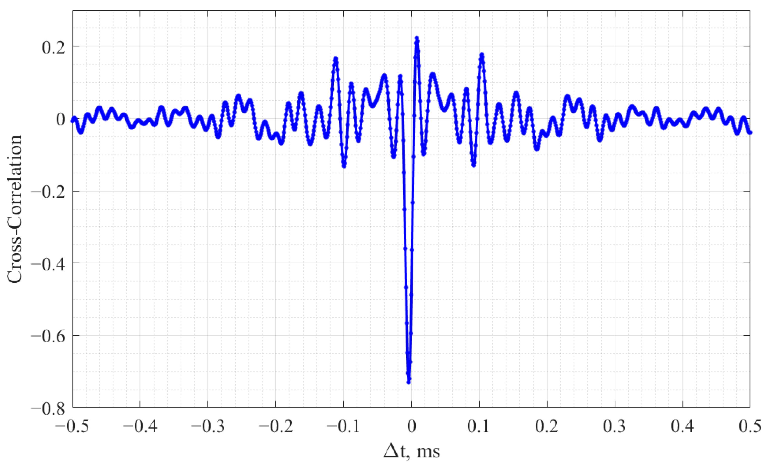
Figure 9 presents the cross-correlation function between
V1 and
V3 for RC two-transistor oscillator.
The bit length is determined as follows—when the cross-correlation function amplitude settles down, the corresponding time shift is selected as the bit length. This approach allows selecting a suitable bit length for the information signal’s transmission. In the given example (
Figure 9), a 110 µs bit length was chosen. Similarly, bit length was determined for Vilnius and Chua’s chaos oscillators (
Table 4).
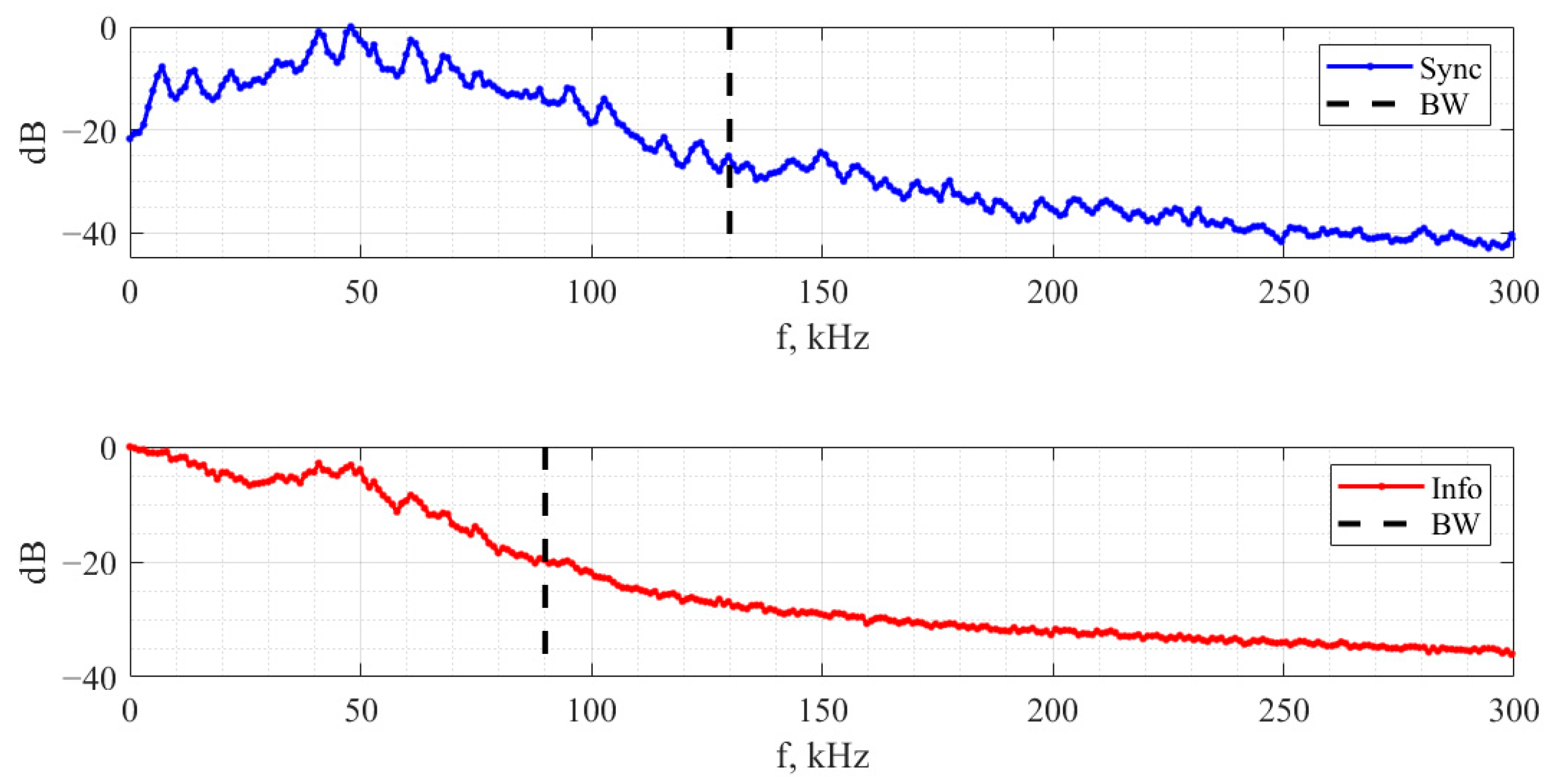
Pre-emphasized information-carrying and synchronization signals modulate the frequency of a carrier. It is essential to select frequency modulation parameters for each communication system using the same approach. The frequency deviation was set to −20 dB level bandwidth of the modulating signal. For example, the RC two-transistor oscillator synchronization signal spectrum and information-carrying signal spectrum are presented in
Figure 10. The bandwidth of the information-carrying signal is 90 kHz, and 130 kHz for the synchronization signal. The selected bandwidth for Vilnius and Chua’s oscillators can be found in
Table 4.
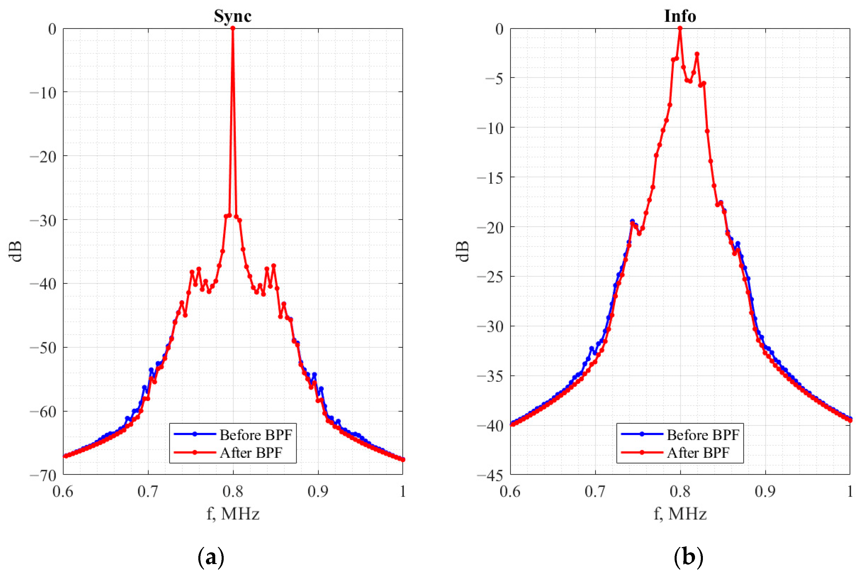
A chaos oscillator, due to inherent nonlinearity, demonstrates initial-conditions-sensitive behavior. Therefore, chaotic signal processing in the FM-CSK communication system should not introduce distortions. It is a ground for the receiver’s bandpass filter selection. A wider filter band is necessary to preserve the chaos signal’s waveform because it is critical for synchronization and chaotic behavior. Thus, a mean square error was used to evaluate the distortion level—the original signal was compared with the frequency demodulated signal after the bandpass filter. The filter’s bandwidth was chosen to ensure a −40 dB mean square error. For both signals, filters are selected separately. For example,
Figure 11a,b show RC two-transistor oscillator synchronization and information-carrying frequency-modulated signal spectra before and after the bandpass filter. The bandpass filter only affects signal components outside the band, so the waveforms are unaffected. The bandpass filter’s band for each oscillator is given in
Table 4.
4.2. Communication System’s Noise Immunity
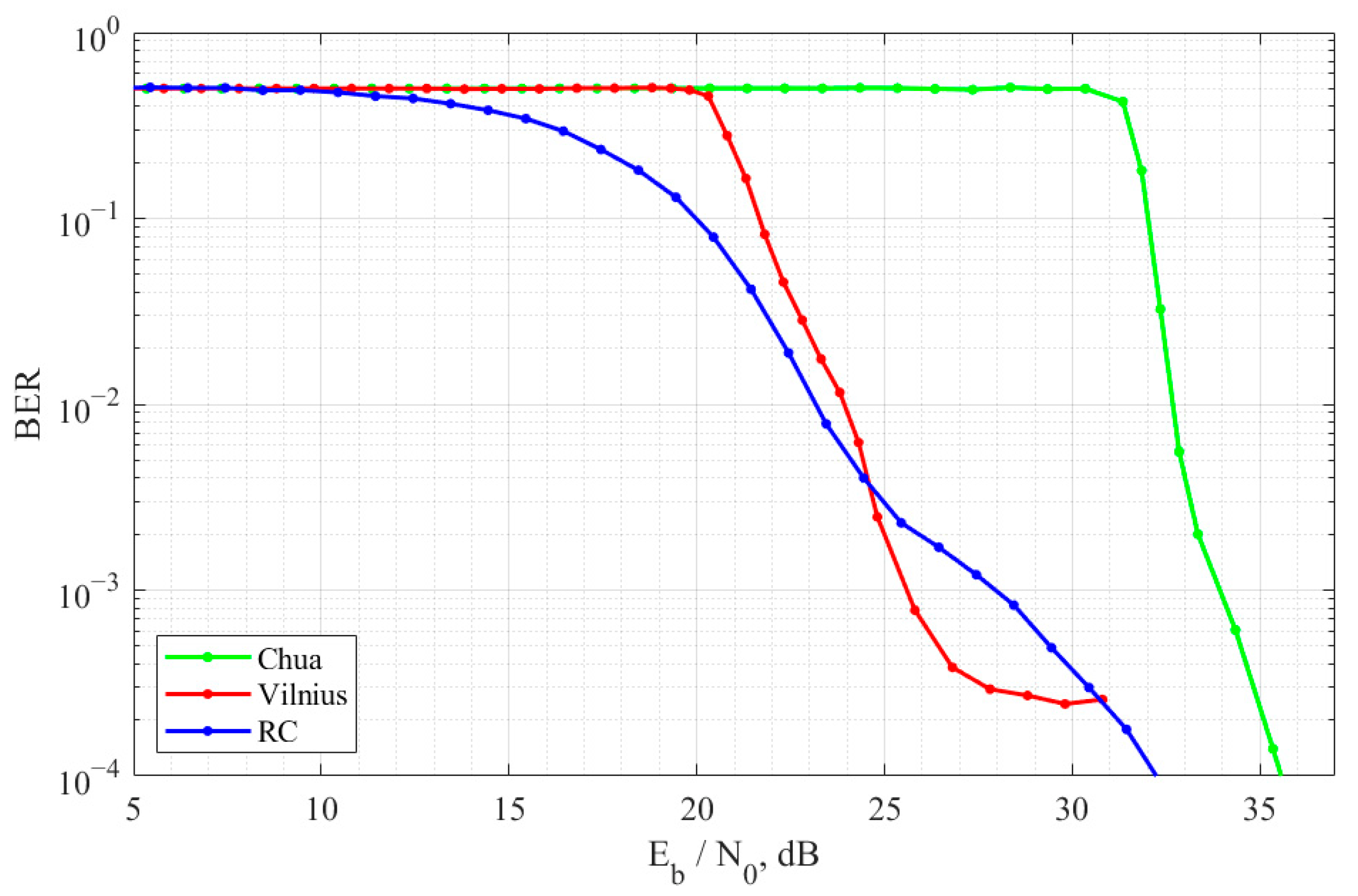
The FM-CSK communication systems based on the discussed chaos oscillators have been compared by estimating their performance in additive white noise channels. As a noise immunity metric of the communication systems based on RC two-transistor chaos oscillator, Vilnius chaos oscillator, and Chua’s chaos oscillator, a bit error ratio (BER) was chosen.
Figure 12 shows experimental results represented by BER curves for each considered communication system. In the case of the RC two-transistor oscillator, the noise immunity analysis result is depicted in blue. The BER of 10% can be obtained for the
Eb/
N0 of 17 dB. For higher signal-to-noise ratio values, the curve shows nearly linear falling with 6.15 powers of ten per decade. In
Figure 12, the red line denotes the BER curves for the communication system based on the Vilnius chaos oscillator. In the
Eb/
N0 ratio region from 20 dB to 27 dB, the curve linearly falls with a steepness of 14.2 powers of ten per decade. A further increase in the signal-to-noise ratio does not lead to a decrease in the error probability, which is explained by the structural features of the communication system, e.g., the operation of the synchronization system. The green curve in
Figure 12 represents the FM-CSK communication system based on Chua’s chaos oscillator noise immunity estimation result. For
Eb/
N0 values from 31 dB to 36 dB, the BER value falls linearly with 20 powers of ten per decade. Note that the selection of parameters of communication systems is made to provide the same correlation properties of chaotic signals of different oscillators within one bit. Thus, the differences in the experimentally obtained BER curves are explained by the cross-correlation and spectral properties of signals generated by chaotic oscillators.
Figure 12 shows that using the RC two-transistor oscillator provides the lowest error probability for a signal-to-noise ratio of less than 25 dB. A communication system based on Chua’s chaotic oscillator needs the highest signal-to-noise ratio to ensure the same error probability.
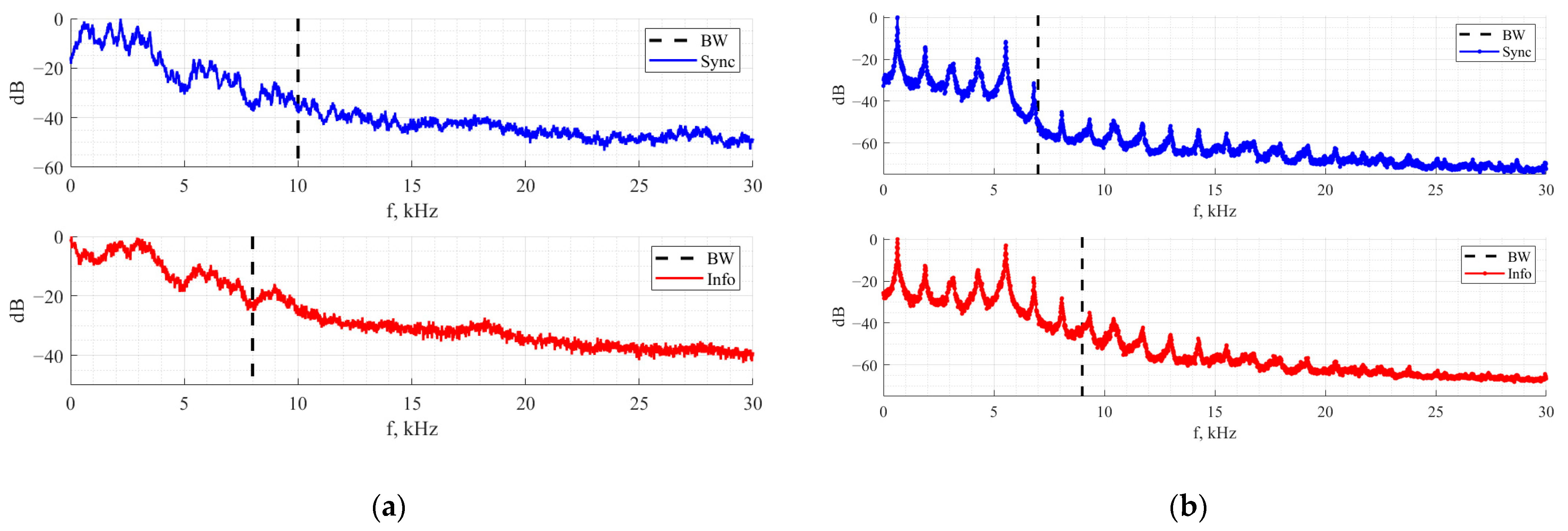
The performance of the observed communication systems corresponds to the properties of power spectral density of the employed chaotic signals. For an RC two-transistor oscillator, both signals’ spectra are presented in
Figure 10. Vilnius and Chua’s chaos oscillator spectra are presented in
Figure 13. The RC signal of the two-transistor oscillator has a uniform spectral distribution of energy in the band and shows a −20 dB reduction in the low-frequency region. On the other hand, Chua’s chaos oscillator spectra have multiple peaks. Thus, a signal with spectral regions that do not carry informational components and are not preliminarily suppressed by the filter gets to the input of the correlator.
The steeper slope of the BER curve is explained by the significant influence of the noise components in these spectral regions. A similar situation is typical for a communication system based on the Vilnius oscillator. In a communication system based on this oscillator, the bandpass filter does not suppress frequencies of 5–7 kHz, where the information components of the signal have low power. The BER curves are also affected by different cross-correlation values at zero shift.


 ,
, 


