Abstract
A systematic and simple approach to develop a 20 W audio frequency range switch mode amplifier is presented in this paper. A non-linear sliding mode (SM) technique-based low cost analog controller enables the realized amplifier to deliver highly linear and efficient operation throughout the audio frequency spectrum. The theoretical aspects and practical limitations in the design and realization of subsystems, such as the signal conditioning stage, power stage and sliding mode controller, are considered, while the viable solution is also stated and justified. The hardware realization scheme is also elaborated, based on which the laboratory prototype is fabricated. Hardware results with a 4 resistive load are given on which the performance of the amplifier is evaluated. The total harmonic distortion (THD) below 1% and 73% efficiency at peak load make the amplifier well suited for high quality audio application.
1. Introduction
The clear and faithful sound of a home audio system is vital for a good listening experience. Basic equipment employed to fill a venue with quality sound are an audio amplifier and loudspeaker. On receiving signal from an audio source (mic, CD/DVD, pen drive, etc.), the audio amplifier amplifies the input signal with the desired gain. The amplified signal is then applied to the loudspeaker, which extracts power from the amplifier to produce sound.
For the accurate reproduction of sound, the linearity of an audio amplifier in the frequency band of 20 Hz to 20 kHz is the decisive feature. Linear amplifiers (Classes A, B, and AB) used in low-power audio applications offer high linearity but suffer from poor efficiency. The class AB amplifier is widely used among linear amplifiers due to its high efficiency and highly linear operation; however, at the actual listening level, the efficiency rarely exceeds 20% [1]. Other amplifiers classes, such as Classes D, E and F, also exist. Class E and Class F amplifiers are highly efficient but they find applications in radio frequency and microwave range [2]. The Class D amplifier exhibits high efficiency, which makes it well suited for audio applications.
With the advent of Class D technology, the audio industry is on the verge of replacing conventional analog amplifiers with switch mode amplifiers. The driving force behind the paradigm shift is close to efficiency of switch mode operation [3,4]. Highly efficient Class D amplifiers, besides having greater run time for battery-powered audio devices, also provide the benefit of compact size and high portability, even for high-power audio applications [5].
Open loop architecture-based Class D amplifiers, though highly efficient, suffer from poor linearity. Besides device non-ideality, such as rise/fall time, turn on/off time and turn on/off delay, etc., the half/full bridge power stage is chiefly responsible for reduced linearity of the amplifier [6]. Additionally, the conventional pulse width modulation (PWM) based audio amplification technique demands a highly accurate triangle carrier generator for satisfactory audio performance [6,7,8]. Additionally, the open loop architecture introduces low frequency power supply noise, which severely degrades the audio quality of amplifier [6]. All the drawbacks associated with open loop architecture and amplifier topology limits the use of Class D amplifier to low quality audio applications.
Closed loop operation can deliver improved linearity performance, high disturbance rejection and noise immunity. However to realize a PWM-based closed loop controlled amplifier demands unrealistic open loop bandwidth, around 20 MHz, and a high frequency carrier generator for audio grade amplification. For the same reason, a closed loop controlled amplifier using the PWM technique becomes unpractical [9,10]. A non-linear controller, such as a hysteresis controller, has much wider control bandwidth, equal to switching frequency, in comparison to linear controller [11]. However, such an amplifier suffers from poor audio quality and the low disturbance rejection problem [6,11,12,13,14,15]. Using sliding mode control (SMC), the non-linear control technique, the closed loop operation can be realized at a significantly lower switching frequency [6,11,15]. Additionally, the advantages of high immunity to parameter variation, accurate reference tracking and no requirement of carrier signal [16,17,18,19,20] led to the selection of the SM technique for controlling the amplifier. Besides these, the simple circuit realization with low component count in designing controller gave motivation to use the SM technique for the development of a highly efficient, mid-power audio amplifier.
For effective description of presented work, the organization of the paper is given as follows. Section 1 discusses the theoretical aspects to develop the constituent blocks of the amplifier. A detailed discussion on the power stage parameters, functioning of the controller and decision on the control parameters is presented in this section. On the basic of selected parameters, the selection of active/passive components and realization of hardware is presented in Section 2. Performance validation is done by extensive testing of the amplifier. A series of tests were carried out to judge the efficiency, linearity and disturbance/noise rejection property of the amplifier, which are described in Section 3. To validate the suitability of the amplifier for actual conditions, the amplifier was tested with a loudspeaker load. The sample results of these tests are discussed in same section. On the basis of the theoretical/practicals aspects, performance and shortcomings of the amplifier, a brief conclusion is given in Section 5 of the paper.
2. Amplifier Development
The sliding mode controlled amplifier (SMCA) consists of the signal conditioning stage and amplification stage. The signal conditioning stage (SCS) of SMCA receives input audio signal, , from the audio source. The output of SCS is pre-amplified signal, , which is applied to the main amplification stage for power amplification. The output of the main amplifier then drives the loudspeaker. The detailed working of each SMCA stage is described in the following sections.
2.1. Signal Conditioning Stage
Figure 1 illustrates the block diagram of the SCS. Pre-amplification of the pre-amplified signal and signal biasing are the main functions of this block.
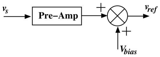
Figure 1.
SCS block diagram.
The pre-amp block amplifies the input audio signal, , with desired gain, while the adder circuit augments the amplified signal with positive/negative dc bias. Biased signal, , serves as a reference to the main amplifier.
2.2. Amplification Stage
The amplification stage, core of the amplifier, enhances the RMS voltage of the incoming reference signal, . The output of the amplification stage powers the loudspeaker system with an amplified signal, which transforms the audio signal into an acoustic signal. The amplification stage of SMCA consists of a band limited output stage and a non-linear controller. The description of these constituents and overall control scheme is presented in the following subsections. The schematic of the band limited output stage is shown in Figure 2. The power stage (PS) of the switching amplifier constitutes complementary switches S1, S2, arranged in a half bridge configuration, and voltage source, .
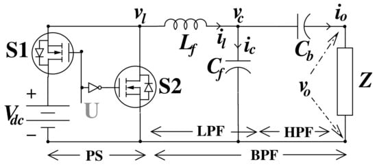
Figure 2.
Output stage of audio amplifier.
The output voltage, , of the power stage is the pulse density modulated (PDM) signal of amplitude . To extract amplified audio signal, , from PDM signal, , a band pass filter (BPF) is cascaded with the PS. The BPF is formed using high pass (HPF) and low pass (LPF) filters whose corner frequencies, and , respectively, determine the lower and upper limits of the BPF. For this application, corner frequencies and , listed in Table 1, are chosen to accommodate the full audio band. The LPF consists of the inductor, , and capacitor, . To render high pass characteristics, the capacitor, , and load impedance Z are utilized. The value of passive components chosen to realize HPF and LPF are listed in Table 1.

Table 1.
, and component values of BPF [21].
Frequency response of the transfer function, (is given in Figure 3) with the loudspeaker load, modeled as a 4 resistor, to mimic its low frequency behavior. It clearly highlights the complete audio band coverage by the BPF.
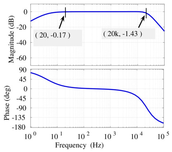
Figure 3.
Frequency response of band pass filter.
The state space equations [22] of the output stage are given as
where
and
The voltage drives the loudspeaker, which transforms the electrical signal into the audio output. The low-frequency component of the speaker current, , is related to the amplifier output as
Control Strategy
The closed loop strategy of SMCA is shown in Figure 4.
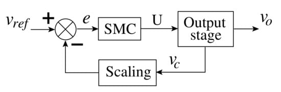
Figure 4.
Block diagram for closed loop control of SMCA.
The reference and scaled output voltage are applied to the summer block. Here, () is the scale factor which yields the desired amplifier voltage gain of . The summer block constitutes a comparator, which produces error signal (e). This signal, e, when applied to the SMC, results in the plant input, U, which is given by (5).
The state vector, , is given by (6).
Phase portraits of the states (, ), for control input and , are depicted in Figure 5.
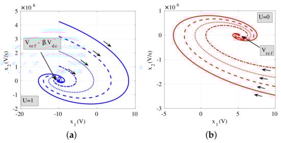
Figure 5.
Phase portrait when (a) ON (b) ON.
When , the upper switch S1 is on, and states and , starting from the arbitrary state, converge at point () of the state space. For , the lower switch S2 turns on, and the state trajectory starting from any arbitrary location, in state space, finally settles at point (). In the sliding mode control technique, states and form a switching surface, S, around which the control action is determined [16,17,18,19,20,21,22]. The switching surface is defined as
The coefficient in (7) is termed as a sliding coefficient. The coefficient , a control parameter, is chosen to determine the slope of the error trajectory, . Figure 6 depicts a sliding line, which is obtained by setting . The line bisects the entire phase plane, depicted in Figure 6.
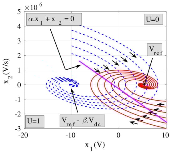
Figure 6.
Phase portrait when and .
The state (, ), belonging to either side of sliding line, is aimed at the line by the controller output U. The control action U, defined as
compels states to hit the sliding line . To ensure that after hitting the sliding line, the phase portrait continues on the sliding line, the following condition, known as the existence condition [16,17,18,19,20,21,22,23,24], must be satisfied
On entering the sliding zone, the state follows the trajectory
to settle at the origin, where refers to the instant when the phase portrait first hits the line . The selection of coefficient is based on the requirement of error minimization for the highest frequency component present in the audio signal. Hence, value , listed in Table 2, is taken such that error minimizes within a quarter cycle of the 20 kHz audio signal. For circuit realization, the switching function, S, is rendered in terms of the circuit parameters as
Table 2.
Amplifier parameters.
However, very high differential gain, , required to realize (11) using op-amps may lead to their saturation [23,25]. Besides very high , the differentiation of noise and switching components in leads to noise amplification, which causes poor audio quality. Hence, using (1), the derivative is replaced by (), and the updated function is given as
The emulated function , besides scaling down the differential gain to unity, ensures the realizable gain of other components using the op-amps. Additionally differentiation of the switching frequency signals and noise is also avoided.
The comparator, depicted in Figure 7a, synthesizes the plant input U to drive the amplifier’s power stage. However, switching devices, such as the transistor and MOSFETs, have finite switching times, which prevent exact synchronization with the comparator output.
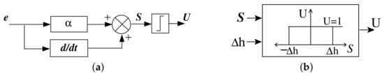
Figure 7.
(a) SMC block (b) Hysteresis block.
To achieve SM operation using finite switching speed devices, the comparator is replaced by a hysteresis band, which, besides assuring quasi-sliding mode operation, also restricts the switching frequency to an arbitrary finite value. The hysteresis block is shown in Figure 7b while the updated switching command is given as
where is the band gap depicted in Figure 7b. The frequency at which the amplifier switches is given as [22,24]
The capacitor voltage, , which ensures precise command following, is
where comprises frequency components in audio range. With the consideration of small signal operation, the substitution of (15) in (14) results in (16), which can be split as
where is the quiescent frequency and denotes excursions around .
Figure 8 depicts the bias point, (), and variation of normalized frequency, , versus the normalized voltage, . The normalized frequency, , and normalized voltage, , are defined as
respectively. This central biasing [26] helps to achieve the maximum amplitude and the lowest possible THD in the output voltage, for a given set of circuit parameters, which has the additional advantage of ensuring least heating of the speaker voice coil. The HPF filters out the DC voltage from the capacitor voltage, , which serves input to the speaker as amplified input voltage, . The parameter values chosen to design the amplifier are tabulated in Table 2.
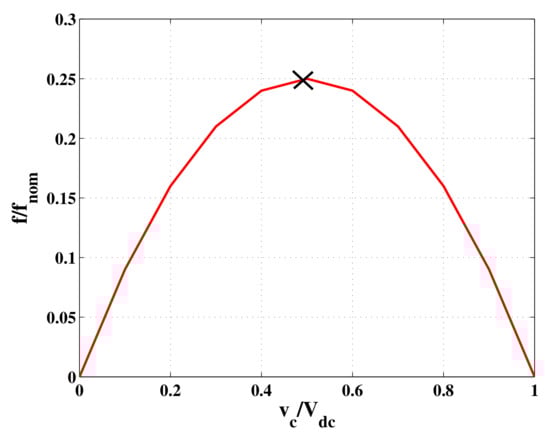
Figure 8.
Plot of normalized voltage versus frequency.
3. Hardware Implementation of SMCA
The schematic of SMCA, shown in Figure 9, comprises three blocks, specifically, the signal conditioning stage (SCS), sliding mode technique-based SM controller (SMC) and output power stage (PS). Active and passive elements, such as op-amps, resistors and capacitors, are utilized to realize the SCS and SMC block. The selection criterion of op-amp are the operating voltage, unity gain-bandwidth, slew rate and noise specification, while the selection of passive components is based on operational requirement. A 60 V, 100 W DC power source, N-channel MOSFET, inductor and capacitor are used to develop the power stage of the amplifier. A detailed discussion on selection of MOSFET is presented in this section, while the selection of the inductor and capacitor was already discussed.
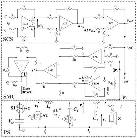
Figure 9.
Control scheme of the audio amplifier.
A feeble input from an audio source is received by the SCS block. On receiving the audio input, the SCS block pre-amplifies the signal. The function of augmenting the DC bias to a pre-amplified audio signal is performed in this block also. The control operation of the amplifier’s output stage is performed by the SMC block. The arithmetic operations, such as scaling, summing, difference, etc., to realize the SCS and SMC block are performed by op-amp using the fixed-value resistors. The operational details of the SCS and SMC block are given as follows. The SCS block utilizes op-amp SC1, SC2 and SC3 to synthesize the reference signal . The op-amp SC1 operates as a fully differential amplifier. The op-amp OPA1632 is chosen to realize SC1. It has a gain bandwidth product of 180 MHz. Increased dynamic range, low input offset voltage and noise immunity are additional features to prefer OPA1632 over the standard op-amp. This op-amp ensures 34 dB single stage gain, a, without injecting any significant noise and offset in the output signal.
The selection of the resistances, R and , to realize gain “a” can be done in many ways. The criterion for selecting the gain setting resistor, for the present case, is explained using Figure 10.
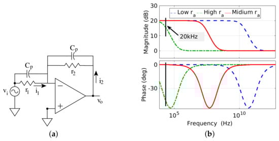
Figure 10.
(a) Op-amp circuit for signal amplification gain “a”. (b) Bode plot of utilizing low, high and medium values of resistance .
Considering a fixed gain of 20 dB, an op-amp based amplification stage is shown in Figure 10a. The gain setting resistor chosen is in the range of tens of ohms, the reason being that the low value of resistance introduces very little thermal noise voltage in the output. The relation between noise voltage, , and resistance is given as
where is the Boltzmann constant (=1.34 × ), T is the temperature in Kelvin (K), B is the bandwidth in Hz, and is the value of the resistance at 300 K (27 C) [27]. The effect of parasitic capacitance, , is another important consideration for selecting a low resistance value. The parasitic capacitance , in order of pF, along with resistances and , is shown in Figure 10a. For , and (=1 pF), Figure 10b depicts gain-phase deviation from the ideal fixed gain over the audio range for low, medium and high values of .
As shown in Figure 10b, using gain setting resistors of low values, the op-amp tracks the desired characteristic (20 dB, ) well beyond the audio spectrum. However, for high output voltage, , gain resistors of low values draw current, , of high magnitude, which pass through the feedback resistance . The general purpose op-amps have a current sourcing capability of a few mA, which causes the device to overload. Prolonged over-loading causes significant power loss and excessive heating of the op-amp, which eventually leads to device failure. Hence, a low value of gain setting resistances is avoided.
Conversely, a very high value (in mega-ohms) of the gain setting resistance leads to significant thermal noise in the input signal of the pre-amplifier. The noisy signal gets amplified by the op-amp effect which has poor input–output linearity. Besides poor linearity, a larger delay between the input–output signal, depicted in Figure 10b, is caused by high gain setting resistances. Because of the problems mentioned above, with a low/high value of the gain setting resistances, a medium value of resistances (in the range of 1–100 K) is chosen here. Advantages of a medium value of resistances are zero phase shift between the input–output signal, shown in Figure 10b, and insignificantly low noise injection in the output signal. The op-amp used to realize amplifier SC2, SC3 is TLE2082, which is a general purpose op-amp. The amplifier SC2 transforms double-ended signal, , into a single ended signal, . Biasing and final amplification of the signal is performed by amplifier SC3. The gain of amplifier SC3 is set at 2. The bias signal, , is fixed at , which ensures biasing of the amplifier at the peak of the normalized frequency versus switching frequency plot, Figure 8.
The signal , coming from the SCS block, becomes the input of the SMC block. acts as the reference for SMCA. The amplifier SM1, realized using TLE2082, compares with the feedback signal to generate error signal, e. The signal , fed back to SM1, is sensed using a resistive network, which is placed across voltage . The resistors and realize a resistive network, which sets the feedback coefficient, , according to (20).
A high value of the resistances, and , is chosen, in the range of , as compared to the loudspeaker load so that the feedback circuit has negligible loading on the amplifier. The scaled differentiation of is performed by the amplifier DEDT. The op-amp used to realize DEDT is OPA4142, an ultra low noise op-amp. The transfer function, , of the realized differentiator is
where
The frequency response of the ideal and actual differentiator is depicted in Figure 11. The value of components and C, listed in Table 3, assure the gain of () in the audio band.
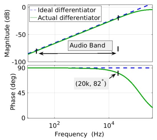
Figure 11.
Magnitude/Phase versus frequency plot of ideal and practical differentiator.
Table 3.
Circuit parameters of SMCA.
Another important feature of the realized differentiator is that the high frequency noise is not amplified. To ensure this, the corner frequency () given by
of DEDT is kept at 120 kHz. Consequently, a phase deviation of , from ideal phase lag of , is observed in the output waveform. The value of to fix at 120 kHz is listed in Table 3.
Realization of sliding function is carried out by amplifier SM2. The sliding function , re-written as follows, realized is the aggregation of the components coming from op-amp SM1, DEDT and IA, respectively, by the adder circuit.
The aggregation function is performed by the adder circuit, which utilizes op-amp TLE2082 to realize SM2 and resistors, R. As already discussed, SM1 supplies error, e, whereas scaled differentiation signal is provided by op-amp DEDT. The third component of sliding function is provided by the instrumentation amplifier (IA). The functioning of amplifier IA is discussed later. The output signal, , of op-amp SM2 is applied to comparator H. The inverting terminal, of the comparator H, is connected to signal , while the non-inverting terminal is connected with a voltage feedback network, which sets the input limit of hysteresis band. Unlike the standard op-amp configured as a comparator, a dedicated comparator IC, with very low response time and high voltage gain is used to compare signal, , with the hysteresis band. The comparator H, which is a high speed, open collector comparator, uses an external pull up resistor, , to drive the high level state at the desired voltage, . The output of the comparator, H, is the control signal, U, the binary levels of which are 0 and volts. The relationship among comparator parameters and hysteresis band, , is given as
and the parameters to render the hysteresis band of 50 mV are listed in Table 3.
The control signal U is then applied to the gate driver. The driver chosen, IC IRS20124, is capable of driving power MOSFETs arranged in a half bridge configuration. Selectable dead time and over-current protection of the switch are inherent features of the gate driver IC. A 45 ns dead time was opted for in the present application. By choosing the recommended value of the resistors selected, dead time was implemented. On receiving control signal U, the driver IC generated pulse G and complementary pulse to drive high and low side MOSFET in the power stage.
The power stage, PS, constitutes the DC source , MOSFETs and and filter network, BPF, formed by aggregating HPF and LPF. The corner frequency and selection of passive components to render high/low pass filter were already discussed. The explanation to realize third component of the sliding function , (24), is given here. The op-amp INA111BU, an instrumentation amplifier (IA), is specifically chosen to realize scaled current . The voltage across shunt resistor , which is placed in the path of current , replicates the down-scaled current . The IA amplifies the voltage across the shunt resistor, , by a fixed gain, G, to realize the desired component of [21]. To ensure desired gain G, of the instrumentation amplifier, an external resistor is chosen in accordance with the following condition.
MOSFET selection is based on the criterion of maximum efficiency. For this purpose, the computation of efficiency, , for available devices having equal drain to source breakdown voltage () is performed as follows
, , and in (27) denote conduction loss, switching loss, gate driver loss and load component, respectively. The test condition for efficiency calculation is listed in Table 4 [21].
Table 4.
Test condition to evaluate efficiency, [21].
The conduction loss, is calculated as
where is the drain source on the resistance of the MOSFET, while the switching loss , (29), has three loss components. The first loss component is due to the finite turn on/off, , time of the MOSFET, while the second loss component is associated with the charging of the output capacitor, . The third loss component is because of the reverse recovery charge, , of the MOSFET body diode.
The gate power loss, at the gate driver operating voltage, , listed in Table 3, is calculated as
where is the charge required by the gate to fully turn on the MOSFET. Based on the operating condition given in Table 4, the loss components, total loss and efficiency, , of the available devices are listed in Table 5.
Table 5.
Loss components and efficiency of the various switching MOSFETs [21].
On the basis of percentage efficiency, listed in Table 5, the IRFI6645 is the most appropriate device for this application. Despite the advantage of high efficiency, the miniaturized footprint of IRFI6645 hinders the mounting of the device on the printed circuit board (PCB). Hence the IRFI4024H-117P, second most efficient device in the Table 5, available in the 5 pin through-hole package, is chosen to fabricate the power stage [21]. In addition to ease in the device mounting, the half bridge configuration of the two n-channel MOSFET in IRFI4024H-117P ensures enhanced noise immunity and compact PCB layout. The greatest advantage of selecting IRFI4024H-117P is no requirement of the heat sink for the presented design.
The power stage is cascaded with the filter network to render the output stage of the amplifier. The controller produces the complementary gate pulses, G and , to switch the devices, S1 and S2, on and off [21]. The switching action of devices resulted in pulse train, . The voltage , a pulse density modulated signal, has a binary level. The high level (HL) equals source voltage , while the low level equalizes with the system ground. The amplifier output , extracted from using the BPF, drives the loudspeaker system.
4. Performance of SMCA with R-Load
Photograph of the experimental set-up which includes amplifier, load, power supply, input signal source and measuring instruments is shown in Figure 12. Overall, three sets of experiments were performed; among them, the 1st set was conducted to evaluate the amplifier’s signal amplification performance. The robustness property of the amplifier was evaluated by the 2nd set of experiments, whereas the disturbance rejection property was probed using the 3rd set of experiments. Details of each set of experiment are given as follows.
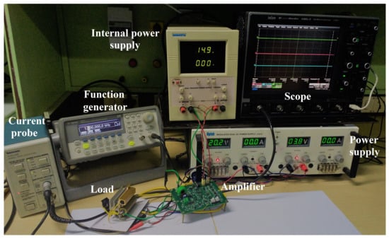
Figure 12.
Experimental setup.
For the first set of experiments, the desired voltage gain of the amplifier was fixed at 28 dB. A , 100 W resistor was used to load the amplifier during these tests. Verification of the amplifier’s gain was done by recording the input–output voltage waveform at 1 kHz. Figure 13a depicts and waveforms at the 1 W power level. The observed gain is 28.6 dB, which is very close to the desired gain, while a phase shift of highlights the amplifier’s impressive command following. Figure 13b depicts the input–output linearity using the frequency spectrum of the output . Clearly, every harmonic component in the spectrum is attenuated to a magnitude lower than 40 dB of the fundamental component, which validates the excellent input–output linearity.
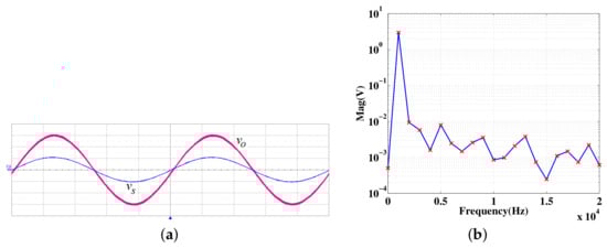
Figure 13.
(a) and waveforms at 1 kHz: (1 volt/div), (0.1 volt/div), timescale: (200 micro-seconds/div) (b) frequency spectrum of 1 kHz output voltage.
To evaluate the extent of the command following and linearity in low and high frequency band of the audio spectrum, the voltage ( and ) waveform and frequency spectrum plot of at frequency 200 Hz and 8 kHz are also presented. Figure 14a depicts the time domain performance of the amplifier at 200 Hz, for which the gain and phase lag are 28.8 dB and 4, respectively. The frequency spectrum is given in Figure 14b, which depicts well-attenuated harmonic components.
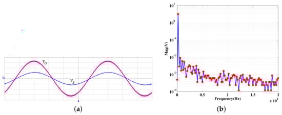
Figure 14.
(a) and waveforms at 200 Hz: (1 volt/div), (0.1 volt/div), timescale: (1 microsecond/div) (b) frequency spectrum of 200 Hz output voltage.
The input–output voltage waveform at 8 kHz is depicted in Figure 15a, the performance metrics are 28.1 dB and −33.3. The harmonic spectrum of at 8 kHz is given in Figure 15b which confirms minimal noise in the output signal. Besides faithful amplification, high linearity of the output signal is evident from these experiments since harmonic components are attenuated to below −40 dB level of the fundamental component.
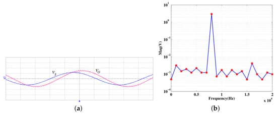
Figure 15.
(a) and waveforms at 8 kHz: (1 volt/div), (0.1 volt/div), timescale: (50 micro-second/div) (b) frequency spectrum of 8 kHz output voltage.
To validate the command following over the entire audio band, a frequency response test was performed. In this test, the frequency of the input signal monotone was swept from 20 Hz to 20 kHz. A schematic of the sweep test is given in Figure 16a. The frequency response analyzer (FRA) sweeps the frequency of the input signal , while keeping its amplitude constant. The input (), output () and frequency data are recorded throughout the sweep. The gain-phase plot of the acquired data is shown in Figure 16b. Clearly, the observed gain of 28.6 dB is in close approximation with the desired value of 28 dB. However, the phase plot reveals the frequency-dependent delay in signal . Excluding the delay, these plots justify the admirable command following by the amplifier.
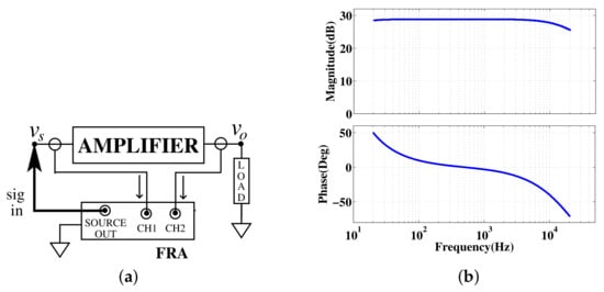
Figure 16.
(a) Schematic for frequency response acquisition, (b) frequency response plot.
To further evaluate linearity of the amplifier, the total harmonic distortion (THD) of the output signal , at 1 W power level, in the 1–10 kHz range was calculated and plotted. Since the amplifier’s input signal, , itself contains harmonic components, an algorithm to accurately calculate the THD of the output signal, , is developed, which is illustrated in Figure 17. Notations used in the algorithm are explained in Table 6.
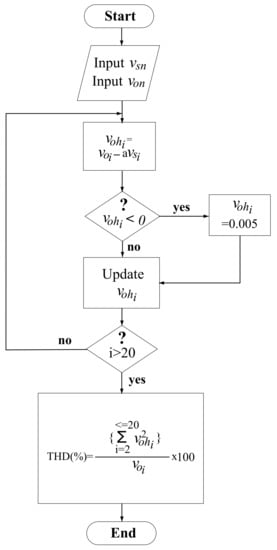
Figure 17.
Algorithm for THD calculation.
Table 6.
Description of the notations in THD algorithm.
The frequency spectrum of the input and output voltage, and , respectively, are recorded from the scope. Using the gain a, given as
the harmonic component, (here, i ranges from to ), in the output voltage, , is calculated as given in Figure 17. Negative components of are replaced by a small positive number (=0.005). Loops shown in Figure 17 ensure updated values of the harmonic components, , which the THD uses, given as
of the output voltage is calculated. The graph of THD versus frequency is depicted in Figure 18. THD well below 1% is observed, within the audio spectrum, which signifies excellent input–output linearity.
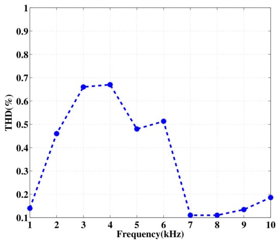
Figure 18.
THD (%) at 1 W.
The amplifier’s performance at the peak load is demonstrated in Figure 19.
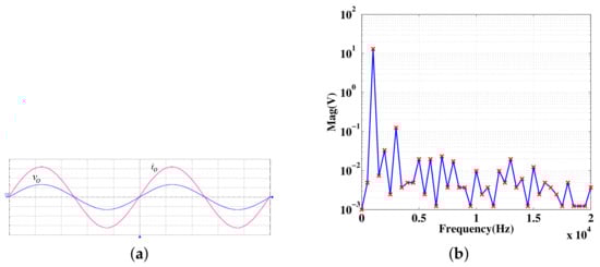
Figure 19.
(a) waveform for 20 W load: (10 volt/div), (1 amp/div), timescale: (200 microsecond/div). (b) Frequency spectrum of output voltage at 20 W.
The input–output waveform, Figure 19a, and frequency spectrum plot of , depicted in Figure 19b, establishes an excellent command following and linearity of the amplifier.
To validate the linearity of the amplifier with actual musical signal, the input, , to output, (), response with the 4 loudspeaker load is given in Figure 20. Since the audio output of the loudspeaker is directly proportional to the speaker current [28,29], thus, the load current, , is taken as the output parameter. Two distinct samples of experimentally obtained speaker current, i, in response to the two arbitrary audio reference signals, , are shown in Figure 20a,b, respectively.
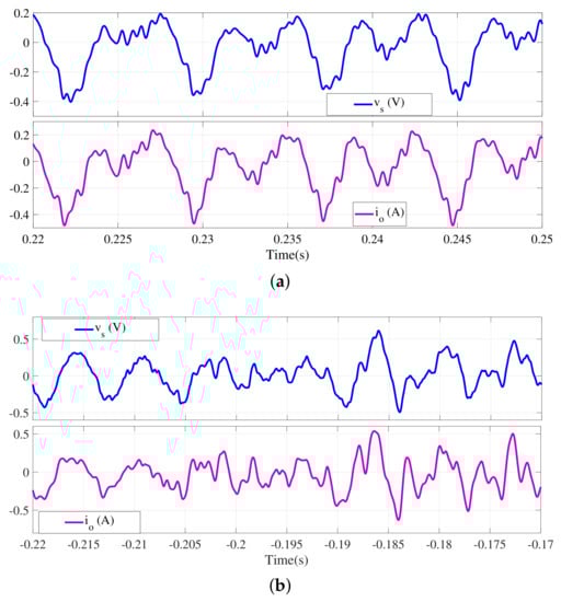
Figure 20.
Experimentally obtained - data. (a) Sample 1. (b) Sample 2.
To evaluate linearity among – quantitatively, the metric sample correlation coefficient [30], , defined as
is used, where and are the standard deviations of the input () and output (i) signals, and is their covariance [30].
The correlation coefficients, , of these two samples, along with three more distinct samples, are given in Table 7. The mean value of over all the sample signals is also stated in the table, which reveals that of the input audio is faithfully converted into acoustic signal.
Table 7.
Correlation coefficient, , between (, ) for musical signal input.
The efficiency plot of the amplifier, in useful audio range, is shown in Figure 21. The test was carried out at peak loading condition; the result obtained exhibited efficiency in the range of to . Efficient performance of amplifier occurred in the frequency range of 500 Hz to 5 kHz.
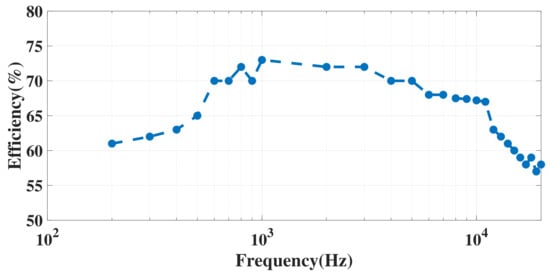
Figure 21.
Efficiency versus frequency plot at 20 W loading.
In the second set of experiments, the robustness property was investigated by applying a step change in the amplifier loading. Figure 22a depicts the waveform , and when subjected to load increment, from 11 W to 14 W (roughly 25% of load addition). Evidently, is unaffected by incremental loading. In addition, Figure 22b depicts the waveform when the amplifier is relaxed by reducing the load from 20 W to 16 W. Undoubtedly, the amplifier output voltage, , remains unaffected from load reduction too.
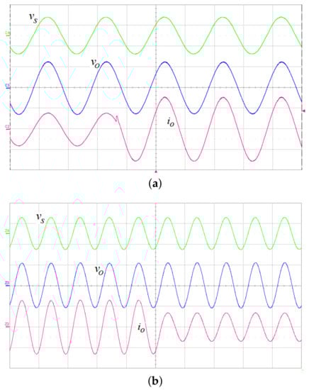
Figure 22.
, and waveform: (0.5 Volt/div), (10 volt/div), (2 amp/div). (a) Incremental loading of amplifier, timescale: (500 micro-second/div). (b) Decremental loading of amplifier, timescale: (1 milli-second/div).
Amplifier’s disturbance rejection property was validated using the third set of experiments. The scheme for the test is depicted in Figure 23.
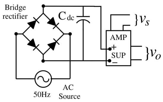
Figure 23.
Disturbance rejection test setup.
The single phase bridge rectifier with relatively small capacitor (=10 F) was chosen as power source () of the amplifier. The DC output voltage of this provisional supply contains ±10% ripple in the output voltage. The frequency spectrum of the source is plotted in Figure 24, which depicts the presence of 100 Hz, 200 Hz, …, components in the DC voltage source.
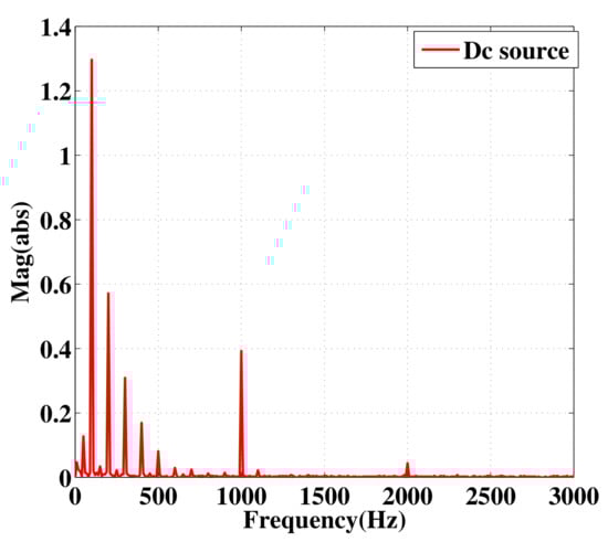
Figure 24.
FFT plot of power source, .
The harmonic component of power source resemble as disturbance signal to the amplifier. To validate the disturbance rejection property of the amplifier, the experiment was performed at 1 W at the 1 kHz level. The captured waveforms are depicted in Figure 25a.
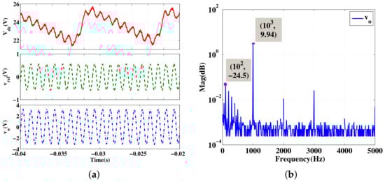
Figure 25.
(a) Waveforms for PSR test. (b) FFT plot of .
From the FFT plot of , Figure 25b, it is confirmed that the disturbance component present in the source imparts a negligible impact on the output voltage. The 100 Hz component of is curtailed at the dB level, while other components (200 Hz, 300 Hz, …,) are attenuated to an even lower level, with a 1 kHz reference audio signal. This shows the superior power supply disturbance rejection quality of the amplifier.
5. Concluding Remark
A systematic approach to develop a 20 W SM control based switch mode audio amplifier is presented. The functioning of each constituent block in the amplifier, design methodology and selection of components are discussed in sufficient detail. With an emphasis on the analog realization of the SM controller, the theoretical and practical aspects of design, such as the selection of sliding coefficient , realization of viable sliding surface S using active and passive components, selection/realization of hysteresis band, deciding the optimal biasing point of the amplifier, etc., are discussed thoroughly. On the basis of the presented design, a 20 W lab prototype is developed. The fabricated amplifier is tested extensively with 4 resistive load. The linearity, robustness and disturbance rejection property of the amplifier are tested. All the results obtained exhibit a high degree of performance to qualify for the high quality audio amplification. With the coil type loudspeaker as the load, the actual musical signal test is conducted on the amplifier, which reveals correlation between the input audio signal and loudspeaker driving current. Further enhancement in the input–output correlation would surely increase the audio quality of audio system.
Author Contributions
Conceptualization, S.J. and M.B.; methodology, S.J.; validation, S.J., R.T. and M.B.; formal analysis, R.K.; investigation, P.K.; writing—original draft preparation, S.J. and R.T.; writing—review and editing, R.K. and P.K. All authors have read and agreed to the published version of the manuscript.
Funding
This research received no external funding.
Data Availability Statement
The datasets supporting the conclusions of this article are included within the article and its additional files.
Conflicts of Interest
The authors declare no conflict of interest.
References
- Pascual, C.; Song, Z.; Krein, P.T.; Sarwate, D.V.; Midya, P.; Roeckner, W.J. High-fidelity PWM inverter for digital audio amplification: Spectral analysis, realtime DSP implementation, and results. IEEE Trans. Power Electron. 2003, 18, 473–485. [Google Scholar] [CrossRef]
- Roshani, S.; Roshani, S. Design of a high efficiency class-F power amplifier with large signal and small signal measurements. Measurement 2020, 149, 106991. [Google Scholar] [CrossRef]
- Self, D. Audio Power Amplifier Design Handbook, 4th ed.; Newnes-Elsevier: Oxford, UK, 2006. [Google Scholar]
- Dapkus, D. Class-D audio power amplifiers: An overview. In Proceedings of the Digest of Technical Papers. International Conference on Consumer Electronics. Nineteenth in the Series (Cat. No.00CH37102), Los Angles, CA, USA, 13–15 June 2000; pp. 400–401. [Google Scholar]
- Guerra, M. Can Class-D Amplifier Audio Performance Get Any Better? 13 October 2016. Electronic Design. Available online: www.electronicdesign.com/analog/can-class-d-amplifier-audio-performance-get-any-better (accessed on 1 January 2018).
- Silva, J.F. PWM audio power amplifiers: Sigma delta versus sliding mode control. In Proceedings of the IEEE International Conference on Electronics, Circuits and Systems. Surfing the Waves of Science and Technology (Cat. No.98EX196), Lisboa, Portugal, 7–10 September 1998; pp. 359–362. [Google Scholar]
- Gaalaas, E. Class D Audio Amplifiers: What, Why and How; Analog Device: Norwood, MA, USA, 2006. [Google Scholar]
- Kao, C.H.; Tsai, P.Y.; Lin, W.P.; Chuang, Y.J. A switching power amplifier with feedback for improving total harmonic distortion. Proc. Analog. Integr. Circuits Signal Process. 2008, 55, 205–212. [Google Scholar] [CrossRef]
- Berkhout, Marco and Dooper, Lûtsen Audio class D amplifiers in mobile application. IEEE Trans. Circuits Syst. I 2010, 57, 1169–1172.
- Liu, Y.H. Novel Modulation Strategies for Class-D Amplifier. IEEE Trans. Consum. Electron. 2007, 53, 987–994. [Google Scholar] [CrossRef]
- Poulsen, S.; Andersen, M.A.E. Hysteresis controller with constant switching frequency. IEEE Trans. Consum. Electron. 2005, 51, 688–693. [Google Scholar] [CrossRef]
- Ji, W.; Qiu, J.; Wu, L.; Lam, H.-K. Fuzzy-Affine-Model-Based Output Feedback Dynamic Sliding Mode Controller Design of Nonlinear Systems. IEEE Trans. Syst. Man Cybern. Syst. 2021, 51, 1652–1661. [Google Scholar] [CrossRef]
- Gui, Y.; Xu, Q.; Blaabjerg, F.; Gong, H. Sliding mode control with grid voltage modulated DPC for voltage source inverters under distorted grid voltage. CPSS Trans. Power Electron. Appl. 2019, 4, 244–254. [Google Scholar] [CrossRef]
- Ma, H.; Li, Y. A Novel Dead Zone Reaching Law of Discrete-Time Sliding Mode Control With Disturbance Compensation. IEEE Trans. Ind. Electron. 2020, 67, 4815–4825. [Google Scholar] [CrossRef]
- Poulsen, S.; Andersen, M.A.E. Self oscillating PWM modulators, a topological comparison. In Proceedings of the Conference Record of the Twenty-Sixth International Power Modulator Symposium, 2004 and 2004 High-Voltage Workshop, San Francisco, CA, USA, 23–26 May 2004; pp. 403–407. [Google Scholar]
- Utkin, V. Variable structure systems with sliding mode. IEEE Trans. Autom. Control 1977, 22, 212–222. [Google Scholar] [CrossRef]
- Utkin, V.; Poznyak, A.; Orlov, Y.; Polyakov, A. Conventional and high order sliding mode control. J. Frankl. Inst. 2020, 357, 10244–10261. [Google Scholar] [CrossRef]
- Utkin, V. Discussion Aspects of High-Order Sliding Mode Control. IEEE Trans. Autom. Control 2016, 61, 829–833. [Google Scholar] [CrossRef]
- Xavier, N.; Bandyopadhyay, B. Practical Sliding Mode Using State Depended Intermittent Control. IEEE Trans. Circuits Syst. II Express Briefs 2021, 68, 341–345. [Google Scholar] [CrossRef]
- Hung, J.; Gao, W.; Hung, J. Variable structure control: A survey. IEEE Trans. Ind. Electron. 1993, 40, 2–22. [Google Scholar] [CrossRef] [Green Version]
- Joshi, S.; Sensarma, P. Fixed frequency based sliding mode controlled audio amplifier. In Proceedings of the 2018 IEEE International Conference on Power Electronics, Drives and Energy Systems (PEDES), Chennai, India, 18–21 December 2018. [Google Scholar]
- Tan, S.; Lai, Y.M.; Cheung, M.K.H.; Tse, C.K. On the practical design of a sliding mode voltage controlled buck converter. IEEE Trans. Power Electron. 2005, 20, 425–437. [Google Scholar] [CrossRef]
- Rojas-Gonzalez, M.A.; Sanchez-Sinencio, E. Design of class D audio amplifier IC using sliding mode control and negative feedback. IEEE Trans. Consum. Electron. 2007, 53, 209–217. [Google Scholar]
- Pillonnet, G.; Cellier, R.; Abouchi, N.; Nagari, A. An integrated class D amplifier based on sliding mode control. In Proceedings of the IEEE Integrated Circuit Design and Technology and Tutorial, Grenoble, France, 2–4 June 2008; pp. 117–120. [Google Scholar]
- Rojas-Gonzalez, M.A.; Sanchez-Sinencio, E. Low power high efficiency class D audio amplifiers. IEEE J. Solid-State Circuit 2008, 44, 3272–3284. [Google Scholar] [CrossRef]
- Joshi, S.; Sensarma, P. Class D audio amplifier with hybrid control. In Proceedings of the 9th International Conference on Power Electronics and ECCE Asia (ICPE-ECCE Asia), Seoul, Korea, 1–5 June 2015; pp. 182–189. [Google Scholar]
- Sedra, A.S.; Smith, K.C. Microelectronic Circuits, 4th ed.; Oxford University Press: New York, NY, USA, 2003. [Google Scholar]
- Mills, P.G.; Hawksford, M.J. Distortion reduction in moving-coil loudspeaker systems using current-drive technology. JAES 1989, 37, 129–148. [Google Scholar]
- Sturtzer, E.; Pillonett, G.; Lemarquand, G.; Abouchi, N. Comparison between voltage and current driving methods of a micro-speaker. Appl. Acoust. 2012, 73, 1087–1098. [Google Scholar] [CrossRef] [Green Version]
- Kreyszig, E. Advanced Engineering Mathematics, 8th ed.; Wiley India (P.) Ltd.: New Delhi, India, 2010. [Google Scholar]
Publisher’s Note: MDPI stays neutral with regard to jurisdictional claims in published maps and institutional affiliations. |
© 2021 by the authors. Licensee MDPI, Basel, Switzerland. This article is an open access article distributed under the terms and conditions of the Creative Commons Attribution (CC BY) license (https://creativecommons.org/licenses/by/4.0/).