Article

Embedded Memories for Cryogenic Applications

1
Department of Computer Engineering, Modeling, Electronics and Systems, University of Calabria, 87036 Rende, Italy
2
Emerging Nanoscaled Integrated Circuits & Systems (EnICS) Labs, Faculty of Engineering, Bar-Ilan University, Ramat-Gan 5290002, Israel
*
Author to whom correspondence should be addressed.
Electronics 2022, 11(1), 61; https://doi.org/10.3390/electronics11010061
Submission received: 30 November 2021 / Revised: 21 December 2021 / Accepted: 23 December 2021 / Published: 25 December 2021
(This article belongs to the Special Issue Design of Ultra-Low Voltage/Power Circuits and Systems)

Abstract

:
The ever-growing interest in cryogenic applications has prompted the investigation for energy-efficient and high-density memory technologies that are able to operate efficiently at extremely low temperatures. This work analyzes three appealing embedded memory technologies under cooling—from room temperature (300 K) down to cryogenic levels (77 K). As the temperature goes down to 77 K, six-transistor static random-access memory (6T-SRAM) presents slight improvements for static noise margin (SNM) during hold and read operations, while suffering from lower (−16%) write SNM. Gain-cell embedded DRAM (GC-eDRAM) shows significant benefits under these conditions, with read voltage margins and data retention time improved by about 2× and 900×, respectively. Non-volatile spin-transfer torque magnetic random access memory (STT-MRAM) based on single- or double-barrier magnetic tunnel junctions (MTJs) exhibit higher read voltage sensing margins (36% and 48%, respectively), at the cost of longer write access time (1.45× and 2.1×, respectively). The above characteristics make the considered memory technologies to be attractive candidates not only for high-performance computing, but also enable the possibility to bridge the gap from room-temperature to the realm of cryogenic applications that operate down to liquid helium temperatures and below.

1. Introduction

Cryogenic electronics is an emerging approach to improve computer performance and deal with the static power consumption issue resulting from transistor scaling towards the end of Moore’s law [1,2,3]. MOS technology operating at cryogenic temperatures provides some benefits, such as steeper subthreshold slope, increased carrier mobility, and increased saturation velocity, leading to semiconductor-based circuits with faster operation, reduced leakage, and improved energy-efficiency [4,5]. As shown in Figure 1, MOS technologies operating at cryogenic temperatures are interesting for a wide spectrum of applications including high-performance computing [6,7], control systems for quantum processors [8,9], and aerospace applications [5,10,11]. The need for electronic devices capable of operating at cryogenic temperatures has always been a sought-after feature in deep space applications; however, high-performance computing and especially quantum computing are now increasing the demand for processors and memories that can operate at very low temperatures. While quantum computing systems operate in the mK range, memory sub-systems capable of operating at the liquid nitrogen boiling point (77 K) and interfacing systems operating at helium temperatures (4 K) are requested as more cost-effective solutions [2,12]. This potentially enables the possibility to bridge the gap from room-temperature to cryogenic applications that operate down to 4 K and below [8].
The benefits of cooling down processors and memory systems to cryogenic temperatures as low as 77 K have recently been demonstrated [2,13,14]. The studies reported in [11,13,15] mainly focus on traditional embedded memories based on six-transistor static random access memory (6T-SRAM), which are shown to provide significant improvements in terms of performance. However, the relatively large bitcell area of 6T-SRAM limits the overall on-chip memory density and the many leakage paths present in these memories limit the achievable power savings [16]. To improve on these issues, other memory technologies like Gain-Cell embedded DRAMs (GC-eDRAMs) and spin-transfer torque magnetic RAMs (STT-MRAMs) were recently proposed as promising candidates for cryogenic computing applications [5,14,16].
GC-eDRAMs has recently been evaluated at 77 K [5,13], showing that it is a viable alternative to 6T-SRAM under cryogenic operation. In addition to the reduced cell area footprint, the refresh power of GC-eDRAMs is highly reduced at 77 K thanks to the suppressed MOS transistor leakage current when operating at 77 K. This leads to overall static (retention) power savings as compared to 6T-SRAM. In particular, for a 2T mixed pMOS-nMOS GC-eDRAM, the data retention time is found to be in the range of ms, enabling considerable power savings as compared to the room temperature operating condition [5]. GC-eDRAMs based on 3T topology have also been evaluated in [13], demonstrating that cache performance similar to 6T-SRAM can be obtained, while achieving higher density, comparable access speed, and lower power. A recent test-chip of 2T-based GC-eDRAM has been evaluated in the temperature range from 4 K to 300 K for various supply voltages [12]. The prototype shows outstanding improvements, in terms of data retention time, by about six orders of magnitude when cooling down from 300 K to 4 K. Therefore, GC-eDRAMs can be considered as a power-effective solution to build embedded memories operating at cryogenic temperatures.
STT-MRAM based on single-barrier magnetic tunnel junction (SMTJ) operating at 77 K has been demonstrated to be an energy-efficient solution for larger cache sizes [16]. However, due to relatively high switching currents, it suffers from longer write access than 6T-SRAM technology. In addition, for smaller cache sizes, SMTJ-based STT-MRAM exhibits latency and energy penalties under write access. To deal with this, and to further reduce the energy consumption of SMTJ-based STT-MRAMs operating at 77 K, STT-MRAM based on double-barrier MTJ (DMTJ) with two reference layers has also been proposed [17]. In addition, leveraging the thermal stability factor of MTJ devices has also been considered as a promising alternative to build reliable, energy-efficient, and high density STT-MRAMs at 77 K. While this was experimentally demonstrated for SMTJ-based STT-MRAM, as reported by Taiwan Semiconductor Manufacturing Company (TSMC) [14], a DMTJ-based STT-MRAM cryogenic simulation study with such an approach is also reported in [18], suggesting that, in contrast to conventional 6T-SRAM, better energy-efficiency can be achieved even for small-to-large cryogenic embedded memories.
In this paper, we present a comparative evaluation between GC-eDRAM, 6T-SRAM, and STT-MRAM memories when operating at 77 K. The analysis is carried out based on a 65 nm commercial process design kit (PDK) calibrated for 77 K under silicon measurements. For simulating the STT-MRAMs, our study uses state-of-the-art SMTJ and DMTJ Verilog-A compact models [19,20]. The results presented within this study are based on comprehensive bitcell-level simulations carried out through exhaustive Monte Carlo simulations. As the main result of this work, we show the key figure-of-merits of the considered memory technologies when cooled down from 300 K to 77 K. We show that 6T-SRAM offers slight improvements (≈5%) in terms of hold and read static noise margins, while suffering from lower write noise margins (−16%), while GC-eDRAM shows larger read voltage margins and data retention time by about 2× and 900×, respectively. SMTJ- and DMTJ-based STT-MRAMs benefit from higher read voltage sensing margins (36% and 48%, respectively), while exhibiting longer write access times (1.45× and 2.1×, respectively).
The rest of the paper is organized as follows: Section 2 presents a brief review of the considered memory technologies and their operating characteristics when operating at cryogenic temperatures. Section 3 presents the simulation results, with the comparison at 77 K discussed in Section 4. Section 5 concludes this work.

2. Background

The embedded memory technologies considered in this work are shown in Figure 2: (a) 6T-SRAM, (b) two-transistor mixed gain cell nMOS-pMOS (2T NW-PR GC-eDRAM), and (c) STT-MRAM based on SMTJ or DMTJ.
  • 6T-SRAM: It is based on a pair of cross-coupled inverters for storing the volatile data. The cell is accessed for write and read operation by asserting the wordline (WL), and driving bitline (BL) and BL ¯ to opposite logic values for write, or pre-charging them for read. Although this is the most mature embedded memory technology available in the market, it has barely been studied at cryogenic temperatures. Recently, 6T-SRAM was evaluated in [15], showing the different trade-offs in terms of static noise margins.
  • GC-eDRAM: This circuit is most often constructed from two to four transistors, and the dynamic (volatile) data is stored by means of the charge upon a parasitic capacitance, which is commonly referred to as storage node (SN). The 2T mixed nMOS–pMOS GC-eDRAM cell is chosen among different topologies in light of its better performance at 77 K [5]. The write operation is done by asserting the write wordline (WWL) of the nMOS write port (NW) and driving the write bitline (WBL) to VDD (‘1’) or ground (‘0’), so that the charge is transferred to or from the SN. As for the read operation, first the read bitline (RBL) is precharged, and then the pMOS read port (PR) is enabled by asserting the read word line (RWL). If the SN is holding a ‘1’, the RBL is discharged to ground, and if it is a ‘0’, the RBL is maintained at VDD. A recent study experimentally demonstrates the GC-eDRAM capabilities when cooled down from room temperature to the helium nitrogen boiling point [12].
  • STT-MRAM: This bitcell consists of a MOS access transistor and an MTJ that stores the non-volatile information. The MTJ stack is build with a reference layer (RL) and a free layer (FL), sandwiching a thin oxide barrier (tOX). This structure is known as an SMTJ, and presents relatively high switching currents, which impact the bit cell write operation [21]. To deal with this, a possible solution is to use a DMTJ with two reference layers (reference layer top (RLT) and bottom (RLB)) that enhance the total torque acting on the FL, leading to lower switching currents, albeit with increased resistance and reduced tunnel magnetoresistance (TMR) [22,23]. According to the relative orientation of the FL with respect to that of the RL (or RLT in the case of the DMTJ), two states are possible: parallel (P) or antiparallel (AP). For more detailed information on the SMTJ and DMTJ structures, the reader is referred to our previous works [21,24].
    STT-MRAM cells can be built from different topologies, which have been previously evaluated in the works reported in [21]. Among the different bitcell topologies, the most area-efficient are the 1TRC and 1TSC configurations (1TRC and 1TSC are referred to as one-transistor/one-MTJ in reverse connection (RC) and standard connection (SC), respectively) for SMTJ and DMTJ, respectively, as shown in Figure 2c.
Table 1 shows the expected impact of cryogenic temperatures on the considered embedded memory technologies. Conventional 6T-SRAM allows significant improvements in terms of performance and power, mainly due to the faster memory access and reduced leakage currents, albeit with reduced write static noise margin (WSNM). The GC-eDRAM also presents power and performance advantages, while also requiring fewer refresh operations at cryogenic temperatures, due to the reduced leakage currents. That being said, GC-eDRAM is still a dynamic memory technology, such that long data retention still requires refresh operations, which complicate the overall system design. When operating at cryogenic temperatures, the STT-MRAM is expected to provide orders of magnitude better endurance and an improved readout signal (due to the higher tunnel magnetoresistance), at the only cost of higher write energy owing to the increased critical switching currents. Overall, all the considered memory technologies benefit from less bitline resistance and faster peripheral circuity when cooled down to cryogenic temperatures. Note that standalone (off-chip) dynamic random-access memory (DRAM) is also considered as a good candidate for cryogenic computing [7]; however, this work is only focused on embedded memory technologies.

3. Simulation Analysis at Cryogenic Temperatures

The embedded memories taken into consideration within this study are designed using a commercial 65 nm CMOS technology, whose BSIM4.7 transistor models were calibrated at the operation temperature of 77 K. The calibrated models take into consideration the impact of cryogenic temperatures on different process corners, along with cryogenic-temperature dependent equations for different parameters like: leakage (e.g., GIDL), mobility, channel doping, body factor, series resistances, stress effects (on threshold voltage, mobility, body factor), etc. As reported in our previous work [5], while the cryogenic-aware calibrated model is roughly correspondent with the original PDK modeling for the operating point of 300 K, as temperature goes down to 77 K, the calibrated model tracks the silicon wafer measurements much more accurately.
The simulations of the STT-MRAMs use state-of-the-art Verilog-A SMTJ and DMTJ compact models [19,20], with major device parameters that are presented in Table 2. The STT-MRAM compact models are based on physical parameters, which were characterized with experimental prototypes at 300 K. The impact of the cryogenic temperature is taken into account according to the formulations provided in [17].
The simulation analysis reported below is based on extensive Monte Carlo circuit-level simulations of the considered memory technologies operating at 300 K and 77 K. These Monte Carlo simulations consider both CMOS and MTJ variability ( σ / μ ). In particular, for the MTJ devices, the Gaussian distributed variability is 5% for the cross-section area, and 1% for tOX, tOX,T, tOX,B, and tFL [21,25,26]. The variability of the CMOS devices is provided by the statistical models of the cryogenic PDK.

3.1. Static Random-Access Memory (SRAM)

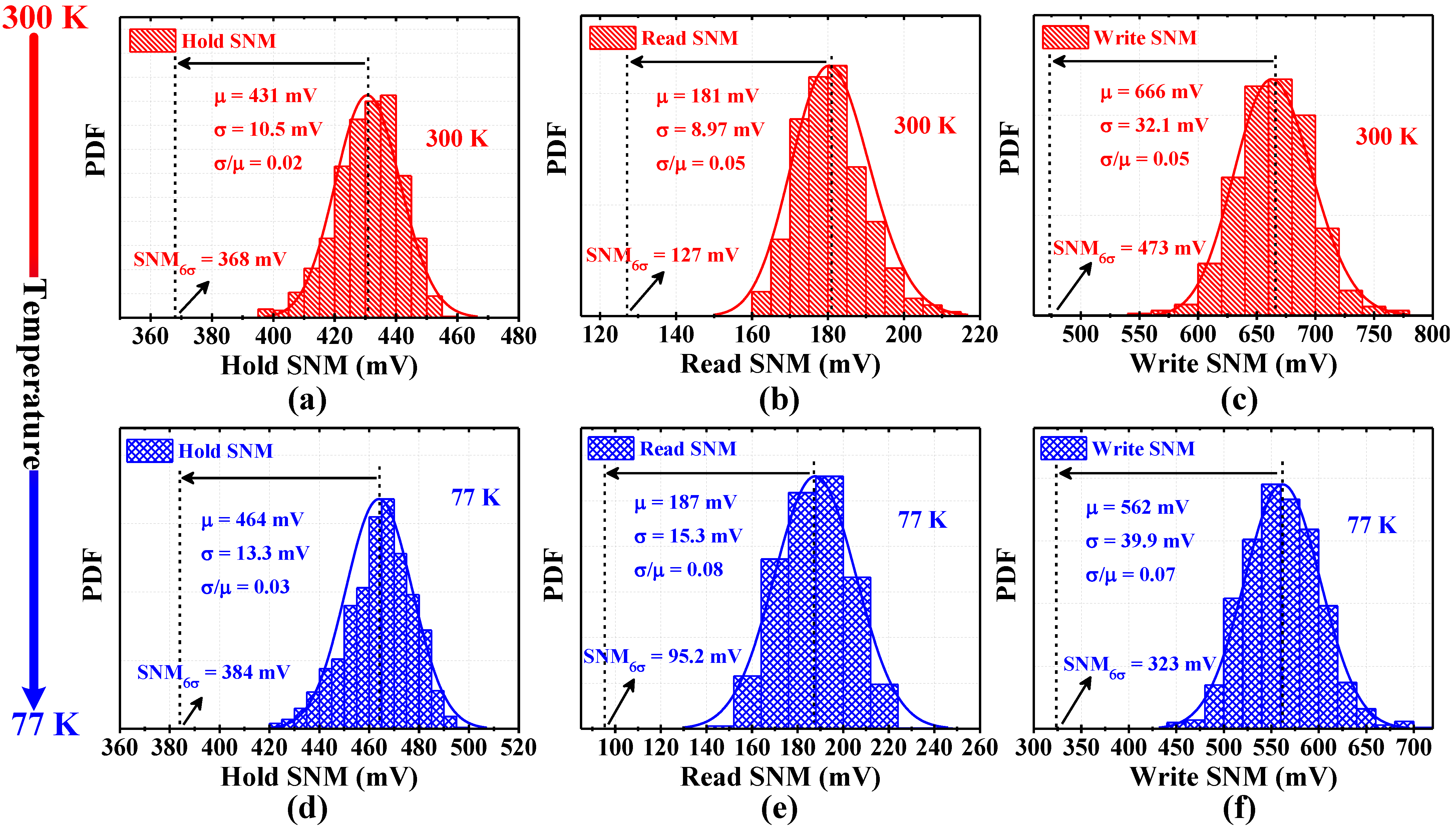
Stability is a crucial design metric in nano-scaled SRAM technologies. Figure 3 shows the statistical distributions of the static noise margin (SNM) for hold (HSNM), read (RSNM), and write (WSNM), when the SRAM is cooled down from 300 K to 77 K. The SNM metrics can be measured by the method proposed by Hill [27]. It consists of plotting the voltage transfer characteristics (VTC) of the SRAM inverters in order to find the noise margins that the SRAM cell can tolerate without disturbing its state. Note that the above method is not efficient for yield results in terms of stability. To deal with this, we used the most-accepted methodology, first proposed by Seevinck et al. [28]. This method efficiently measures the noise margin metrics with a DC sweep simulation. In particular, measuring noise margins (HSNM, RSNM, WSNM) distributions provides a reliable yield estimation, typically at 6 σ , which is required for the design of high-density SRAM cells [29].
HSNM and RSNM consider the measure of the largest DC voltage that the SRAM cell can withstand without flipping the stored state. As for the WSNM, it is the minimum voltage required for the SRAM cell to be in a monostable state [29]. While the HSNM is measured with the WL tied to ground, for the RSNM and WSNM the WL is asserted while bitlines are driven to VDD and opposite logic values, respectively.
As compared to the 300 K operating temperature, at 77 K the HSNM and RSNM present a slight increase of about 7.66% and 3.31%, respectively. While this result is obtained at a nominal VDD of 1.2 V, the HSNM and RSNM can be improved when operating at lower VDD [15]. In particular, when operating in the subthreshold (VDD = 0.3 V) region, the HSNM and RSNM increase by about 2× and 4×, respectively. This is due to the steeper transition of the data storage nodes at 77 K [15]. As for the WSNM, it degrades by 15.6% at 77 K due to the increased strength of the SRAM cell pull-up network at the low temperature.

3.2. Gain-Cell Embedded DRAM (GC-eDRAM)

As opposed to 6T-SRAM, which has one universally accepted bitcell topology, previous GC-eDRAM research has suggested a large variety of configurations, depending on the target specifications and technology node. In our previous work [5], we demonstrated that the mixed configuration nMOS-pMOS (2T NW-PR) GC-eDRAM cell represents the best solution at 77 K for the considered 65 nm technology. Note that the following GC-eDRAM results in terms of voltage margins and data retention capabilities were evaluated in the worst-case condition. That is, when the WBL is driven to VDD or ground while the SN is ‘0’ or ‘1’, respectively.
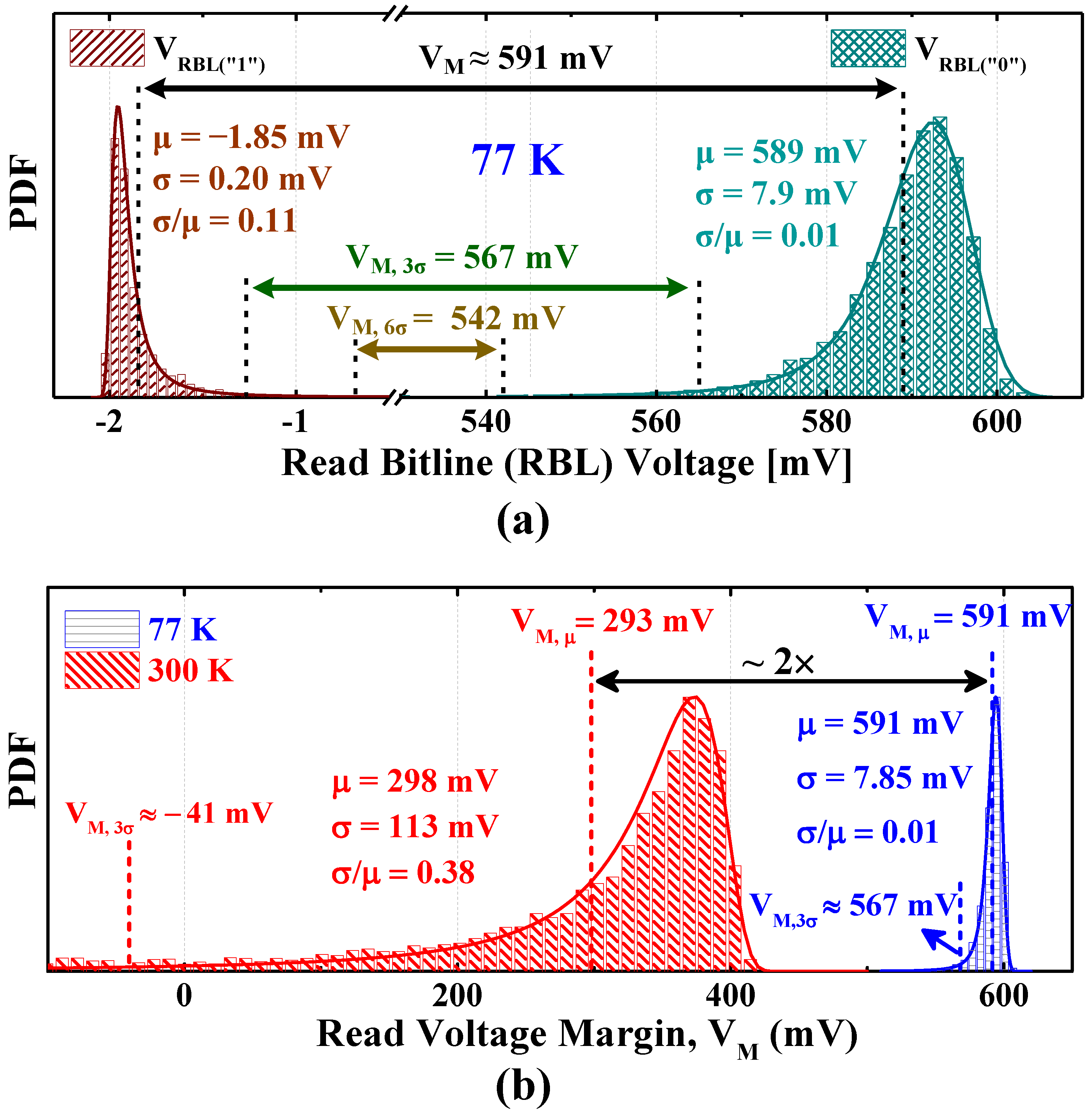
Figure 4a shows the statistical distributions of the read bitline voltages when the SN is holding a ‘1’ ( V R B L ( 1 ) ) or ‘0’ ( V R B L ( 0 ) ) at an operating temperature of 77 K and considering a read pulse of 1 ns. The voltage margin V M , which is defined as the difference between the RBL voltage for ‘1’ and ‘0’ (i.e., V M = V R B L ( 1 ) V R B L ( 0 ) ), is measured at 4 µs after writing into the SN.
The figure shows the V M evaluated at both 3-sigma and 6-sigma with considerably high margins when operating at 77 K. Moreover, Figure 4b shows the statistical distributions of the read voltage margin corresponding to the mean values measured in Figure 4a. In addition to V M at 77 K, 300 K is also considered, to better show the benefits in terms of voltage margins when the GC-eDRAM operates under cryogenic conditions. In particular, V M at 77 K is improved by 2 × as compared to 300 K simulation results.
Because of the inherently dynamic characteristics of the GC-eDRAM, periodic refresh operations are required. However, since the subthreshold leakage is substantially suppressed at cryogenic temperatures, the memory retention time is expected to be considerably improved. Accordingly, we extended our analysis on the considered 2T GC-eDRAM cell to evaluate the data retention capabilities. Figure 5a,b show the worst-case storage node deterioration after writing ‘0’/‘1’ into the 2T GC-eDRAM when operating at 300 K and 77 K, respectively. While the blue curves show the degeneration of a logic ‘1’ level when WBL is driven to ground, the red curves show the degeneration of the logic ‘0’ level with WBL driven to VDD. As compared to the 300 K simulations, the 77 K operating point shows improvements by orders of magnitude. In particular, it can be seen that the SN degeneration at cryogenic temperatures is in the order of ms, which points out that energy-wasting refresh operations could be considerably limited. This is further emphasized by Figure 5c, which shows the statistical distribution of the data retention time (DRT) at 300 K and 77 K. Here, we define DRT as the time it takes for the difference between the ‘0’ and ‘1’ SN voltages, reported in Figure 5a,b, to be 200 mV [30]. At 77 K, the DRT is improved by 900 × with respect to room temperature simulations, while also exhibiting 98% less variability.

3.3. Spin-Transfer Torque Magnetic RAM (STT-MRAM)

The 1TRC and 1TSC bitcell configurations were referenced in this work since they are the most cost-effective solutions in terms of area and energy to build STT-MRAM embedded memories based on SMTJ and DMTJ, respectively [21]. Figure 2c shows the 1TRC and 1TSC configurations, where the RL (for the SMTJ) or RLB (for the DMTJ) are connected to the BL.
Monte Carlo simulation results under write and read accesses are shown in Figure 6 and Figure 7 for both SMTJ- and DMTJ-based STT-MRAM cells. The reported results refer to 300 K and 77 K simulations, while considering a write error rate (WER) and read disturbance rate (RDR) of 10 7 and 10 9 , respectively [31]. In particular, Figure 6 shows the statistical distribution of the write pulse (tp) referred to the worst case between AP→ P and P→ AP transitions. When cooling down to 77 K, we can observe a penalty of about 1.45× and 2.1× in terms of tp for SMTJ- and DMTJ-based bitcells. This is because the critical switching current dramatically increases as temperature goes down to cryogenic levels [16,17,32], with an adverse impact on energy and latency for write operation. This can be counterbalanced by increasing the width of the access transistor. Note that tp is evaluated at 6-sigma ( t p , 6 σ ). Although SMTJ- and DMTJ-based STT-MRAM solutions present an increased tp of more than 50% as compared to the 300 K operating point, STT-MRAM based on DMTJ allows a tp of a few ns, even for cryogenic temperatures.
To evaluate the reading performance of STT-MRAMs, we used the conventional voltage sensing (CVS) scheme [33], which includes applying a fixed read current (Iread) to the BL of the bitcell, and then comparing the BL voltage (VBL) with a reference voltage (VREF) by means of a sense amplifier. Iread is set to be low enough to not disturb the stored data ( R D R = 10 9 ) (A read pulse width (tread) of 1 ns is considered). Figure 7 shows the statistical distribution of the bitline voltages for SMTJ- and DMTJ-based STT-MRAM bitcells operating at 300 K and 77 K. From the two sensing operations, V B L ( P ) and V B L ( A P ) , the voltage sensing margin (VSM) is defined as: VSM = V B L ( A P ) V B L ( P ) . Due to the rise in the TMR, VSM increases at cryogenic temperatures as compared to 300 K [14,32]. In particular, from Figure 7, we can observe VSM improvements by about 36% and 48% for the SMTJ- and DMTJ-based STT-MRAMs. Note that, the DMTJ-based bitcell has reduced sensing margins with respect its SMTJ-based counterpart. In both the cases, the sensing margins can be improved by adopting proper BL boosting design techniques [34,35].

4. Comparison Results

In order to complete our analysis and make a direct comparison between the different memory technologies, we have measured their main characteristics, including area, sensing margins, data retention capabilities, read/write access, and both power and energy consumption. Table 3 summarizes the simulation results for a 128-word memory bank operating at 77 K and considering a nominal VDD. Note that the data reported in terms of area corresponds to a standard full-custom design, i.e., not using “pushed rules”.
From Table 3, the STT-MRAM configurations are the most area-efficient solutions, presenting a bitcell area footprint of about 88% and 56% less than the 6T-SRAM and GC-eDRAM, respectively. This characteristic make them very attractive for designing dense, non-volatile embedded memory banks. In terms of sensing margins, the GC-eDRAM is the technology that benefits the most from operating at 77 K, showing V M improvements up to 90%. While the STT-MRAM cells also present improvements in terms of VSM, the 6T-SRAM maintains comparable HSNM and RSNM, along with reduced WSNM. As for the data retention capabilities, while 6T-SRAM and STT-MRAM provide static and non-volatile behavior, respectively, GC-eDRAM exhibits DRTs in the order of ms, allowing reduced refresh operations with respect to the room temperature operating point.
From Table 3, the STT-MRAM is the most penalized in terms of access time, mainly due to larger write time at 77 K. In particular, the DMTJ-based STT-MRAMs suffer from longer write times of about 24×, on average, as compared to 6T-SRAM and GC-eDRAM. In terms of write and read energy, the GC-eDRAM is the most energy-efficient solution, showing write and read improvements of about 63% and 70%, respectively, as compared to 6T-SRAM. However, differently from STT-MRAM and 6T-SRAM, GC-eDRAM still requires energy consuming refresh operations, although much less than the room temperature operation. Finally, the leakage power is also measured in standby mode. While STT-MRAM technology presents almost zero leakage (the only leakage contribution is due to the periphery), 6T-SRAM presents 98% higher leakage power than GC-eDRAM.

5. Conclusions

In this work, we investigated the impact of cryogenic temperatures on different embedded memory technologies. Our study was carried out using a commercial 65 nm 1.2 V CMOS technology fully calibrated under silicon measurements at cryogenic temperatures. Obtained results demonstrate that embedded memory technologies benefit in different figures-of-merit when cooled down from 300 K to 77 K. Although the most commercially mature technology, 6T-SRAM, is faster and less leaky at cryogenic temperatures, its relatively large area footprint and reduced write static noise margin at 77 K are less desired. GC-eDRAM excels in most of figures-of-merit, and even if refresh operations are required, the resulting refresh power is considerably lower than when operating at room temperature. In particular, GC-eDRAM benefits from improved read voltage margins and data retention time by about 2× and 900×, respectively. STT-MRAMs based on SMTJ present high write overhead due to increased switching currents at cryogenic temperatures. However, the DMTJ-based solution significantly reduces the write penalty (by 83%). Furthermore, the readout capability of STT-MRAMs is improved, enabling more reliable read operations at cryogenic temperatures. Overall, our evaluation points out that embedded memory technologies can be interesting for cryogenic applications, not only for high-performance computing, but also for bridging the gap from room-temperature to the realm of cryogenic applications that operate down to liquid helium temperatures and below.

Author Contributions

Conceptualization, E.G., A.T. and M.L.; formal analysis, E.G., A.T. and M.L.; investigation, E.G., A.T. and M.L.; writing—review and editing, E.G., A.T. and M.L. All authors have read and agreed to the published version of the manuscript.

Funding

A. Teman was supported by the Israel Science Foundation under Grant 996/18 and by the Smart Imaging Consortium under the MAGNET program of the Israel Innovation Authority.

Conflicts of Interest

The authors declare no conflict of interest.

Abbreviations

The following abbreviations are used in this manuscript:
6T-SRAMSix-transistor Static Random Access Memory
DRAMDynamic Random-Access Memory
GC-eDRAMGain-Cell embedded DRAM
STT-MRAMSpin-Transfer Torque MRAM
MTJMagnetic Tunnel Kunction
SMTJSingle-barrier MTJ
DMTJDouble-barrier MTJ
TSMCTaiwan Semiconductor Manufacturing Company
PDKProcess Design Kit
SNStorage Node
NWnMOS write port
PRpMOS read port
RLReference Layer
FLFree Layer
TMRtunnel magnetoresistance
Pparallel
APantiparallel
RCReverse Connection
SCStandard Connection
SNMStatic Noise Margin
WSNMWrite SNM
RSNMRead SNM
HSNMHold SNM
VTCvoltage transfer characteristics
DRTData Retention time
WERWrite Error Rate
RDRRead Disturbance Rate
CVSConventional Voltage Sensing
2T NW-PR2T Mixed GC nMOS-pMOS

References

  1. IRDS-IEEE. International Roadmap for Devices and Systems—Cryogenic Electronics and Quantum Information Processing. 2021. Available online: https://irds.ieee.org/editions/2021/cryogenic-electronics-and-quantum-information-processing (accessed on 30 November 2021).
  2. Sanuki, T.; Aiba, Y.; Tanaka, H.; Maeda, T.; Sawa, K.; Kikushima, F.; Miura, M. Cryogenic Operation of 3D Flash Memory for Storage Performance Improvement and Bit Cost Scaling. IEEE J. Explor.-Solid-State Comput. Devices Circuits 2021, 7, 159–167. [Google Scholar] [CrossRef]
  3. Resch, S.; Cilasun, H.; Karpuzcu, U.R. Cryogenic PIM: Challenges amp; Opportunities. IEEE Comput. Archit. Lett. 2021, 20, 74–77. [Google Scholar] [CrossRef]
  4. Balestra, F.; Audaire, L.; Lucas, C. Influence of substrate freeze-out on the characteristics of MOS transistors at very low temperatures. Solid-State Electron. 1987, 30, 321–327. [Google Scholar] [CrossRef]
  5. Garzón, E.; Greenblatt, Y.; Harel, O.; Lanuzza, M.; Teman, A. Gain-Cell Embedded DRAM Under Cryogenic Operation—A First Study. IEEE Trans. Very Large Scale Integr. (VLSI) Syst. 2021, 29, 1319–1324. [Google Scholar] [CrossRef]
  6. Byun, I.; Min, D.; Lee, G.; Na, S.; Kim, J. A Next-Generation Cryogenic Processor Architecture. IEEE Micro 2021, 41, 80–86. [Google Scholar] [CrossRef]
  7. Ware, F.; Gopalakrishnan, L.; Linstadt, E.; McKee, S.A.; Vogelsang, T.; Wright, K.L.; Hampel, C.; Bronner, G. Do Superconducting Processors Really Need Cryogenic Memories? The Case for Cold DRAM. In Proceedings of the International Symposium on Memory Systems, Alexandria, Virginia, 2–5 October 2017. [Google Scholar] [CrossRef] [Green Version]
  8. Patra, B.; Incandela, R.M.; Van Dijk, J.P.; Homulle, H.A.; Song, L.; Shahmohammadi, M.; Staszewski, R.B.; Vladimirescu, A.; Babaie, M.; Sebastiano, F.; et al. Cryo-CMOS circuits and systems for quantum computing applications. IEEE J. Solid-State Circuits 2017, 53, 309–321. [Google Scholar] [CrossRef] [Green Version]
  9. Sebastiano, F.; Homulle, H.A.; van Dijk, J.P.; Incandela, R.M.; Patra, B.; Mehrpoo, M.; Babaie, M.; Vladimirescu, A.; Charbon, E. Cryogenic CMOS interfaces for quantum devices. In Proceedings of the 2017 7th IEEE International Workshop on Advances in Sensors and Interfaces (IWASI), Vieste, Italy, 15–16 June 2017; IEEE: Piscataway, NJ, USA, 2017; pp. 59–62. [Google Scholar] [CrossRef]
  10. Deane, S.; Avdelidis, N.P.; Ibarra-Castanedo, C.; Zhang, H.; Yazdani Nezhad, H.; Williamson, A.A.; Mackley, T.; Maldague, X.; Tsourdos, A.; Nooralishahi, P. Comparison of cooled and uncooled IR sensors by means of signal-to-noise ratio for NDT diagnostics of aerospace grade composites. Sensors 2020, 20, 3381. [Google Scholar] [CrossRef] [PubMed]
  11. Barlow, M.; Fu, G.; Hollosi, B.; Lee, C.; Di, J.; Mantooth, H.A.; Schupbach, M.; Berger, R. A PFET-access radiation-hardened SRAM for extreme environments. In Proceedings of the 2008 51st Midwest Symposium on Circuits and Systems, Knoxville, TN, USA, 10–13 August 2008; IEEE: Piscataway, NJ, USA, 2008; pp. 418–421. [Google Scholar] [CrossRef]
  12. Saligram, R.; Datta, S.; Raychowdhury, A. CryoMem: A 4K-300K 1.3 GHz eDRAM Macro with Hybrid 2T-Gain-Cell in a 28nm Logic Process for Cryogenic Applications. In Proceedings of the 2021 IEEE Custom Integrated Circuits Conference (CICC), Austin, TX, USA, 25–30 April 2021; IEEE: Piscataway, NJ, USA, 2021; pp. 1–2. [Google Scholar] [CrossRef]
  13. Min, D.; Byun, I.; Lee, G.H.; Na, S.; Kim, J. Cryocache: A fast, large, and cost-effective cache architecture for cryogenic computing. In Proceedings of the Twenty-Fifth International Conference on Architectural Support for Programming Languages and Operating Systems, Lausanne, Switzerland, 16–20 March 2020; pp. 449–464. [Google Scholar] [CrossRef] [Green Version]
  14. Chiang, H.; Wang, J.; Chen, T.; Chiang, T.; Bair, C.; Tan, C.; Huang, L.; Yang, H.; Chuang, J.; Lee, H.; et al. Cold MRAM as a Density Booster for Embedded NVM in Advanced Technology. In Proceedings of the 2021 Symposium on VLSI Technology, Kyoto, Japan, 13–19 June 2021; IEEE: Piscataway, NJ, USA, 2021; pp. 1–2. [Google Scholar]
  15. Hu, V.P.H.; Liu, C.J. Static Noise Margin Analysis for Cryo-CMOS SRAM Cell. In Proceedings of the 2021 IEEE International Symposium on Radio-Frequency Integration Technology (RFIT), Hualien, Taiwan, 25–27 August 2021; IEEE: Piscataway, NJ, USA, 2021; pp. 1–2. [Google Scholar] [CrossRef]
  16. Garzón, E.; De Rose, R.; Crupi, F.; Teman, A.; Lanuzza, M. Exploiting STT-MRAMs for cryogenic non-volatile cache applications. IEEE Trans. Nanotechnol. 2021, 20, 123–128. [Google Scholar] [CrossRef]
  17. Garzón, E.; De Rose, R.; Crupi, F.; Carpentieri, M.; Teman, A.; Lanuzza, M. Simulation Analysis of DMTJ-Based STT-MRAM Operating at Cryogenic Temperatures. IEEE Trans. Magn. 2021, 57, 1–6. [Google Scholar] [CrossRef]
  18. Garzón, E.; De Rose, R.; Crupi, F.; Trojman, L.; Teman, A.; Lanuzza, M. Relaxing non-volatility for energy-efficient DMTJ based cryogenic STT-MRAM. Solid-State Electron. 2021, 184, 108090. [Google Scholar] [CrossRef]
  19. De Rose, R.; Lanuzza, M.; d’Aquino, M.; Carangelo, G.; Finocchio, G.; Crupi, F.; Carpentieri, M. A compact model with spin-polarization asymmetry for nanoscaled perpendicular MTJs. IEEE Trans. Electron Devices 2017, 64, 4346–4353. [Google Scholar] [CrossRef]
  20. De Rose, R.; d’Aquino, M.; Finocchio, G.; Crupi, F.; Carpentieri, M.; Lanuzza, M. Compact modeling of perpendicular STT-MTJs with double reference layers. IEEE Trans. Nanotechnol. 2019, 18, 1063–1070. [Google Scholar] [CrossRef]
  21. Garzón, E.; De Rose, R.; Crupi, F.; Trojman, L.; Finocchio, G.; Carpentieri, M.; Lanuzza, M. Assessment of STT-MRAMs based on double-barrier MTJs for cache applications by means of a device-to-system level simulation framework. Integration 2020, 71, 56–69. [Google Scholar] [CrossRef]
  22. Hu, G.; Lee, J.H.; Nowak, J.J.; Sun, J.Z.; Harms, J.; Annunziata, A.; Brown, S.; Chen, W.; Kim, Y.H.; Lauer, G.; et al. STT-MRAM with double magnetic tunnel junctions. In Proceedings of the 2015 IEEE International Electron Devices Meeting (IEDM), Washington, DC, USA, 7–9 December 2015; pp. 26.3.1–26.3.4. [Google Scholar] [CrossRef]
  23. Garzón, E.; Lanuzza, M.; Taco, R.; Strangio, S. Ultralow voltage finFET-versus TFET-based STT-MRAM cells for IoT applications. Electronics 2021, 10, 1756. [Google Scholar] [CrossRef]
  24. Garzón, E.; De Rose, R.; Crupi, F.; Trojman, L.; Lanuzza, M. Assessment of STT-MRAM performance at nanoscaled technology nodes using a device-to-memory simulation framework. Microelectron. Eng. 2019, 215, 111009. [Google Scholar] [CrossRef]
  25. Zhang, Y.; Zhao, W.; Lakys, Y.; Klein, J.; Kim, J.; Ravelosona, D.; Chappert, C. Compact Modeling of Perpendicular-Anisotropy CoFeB/MgO Magnetic Tunnel Junctions. IEEE Trans. Electron Devices 2012, 59, 819–826. [Google Scholar] [CrossRef]
  26. Wang, G.; Zhang, Y.; Wang, J.; Zhang, Z.; Zhang, K.; Zheng, Z.; Klein, J.; Ravelosona, D.; Zhang, Y.; Zhao, W. Compact Modeling of Perpendicular-Magnetic-Anisotropy Double-Barrier Magnetic Tunnel Junction With Enhanced Thermal Stability Recording Structure. IEEE Trans. Electron Devices 2019, 66, 2431–2436. [Google Scholar] [CrossRef]
  27. Hill, C. Noise margin and noise immunity in logic circuits. Microelectronics 1968, 1, 16–21. [Google Scholar]
  28. Seevinck, E.; List, F.J.; Lohstroh, J. Static-noise margin analysis of MOS SRAM cells. IEEE J. Solid-State Circuits 1987, 22, 748–754. [Google Scholar] [CrossRef] [Green Version]
  29. Teman, A.; Mordakhay, A.; Mezhibovsky, J.; Fish, A. A 40-nm sub-threshold 5T SRAM bit cell with improved read and write stability. IEEE Trans. Circuits Syst. II: Express Briefs 2012, 59, 873–877. [Google Scholar] [CrossRef]
  30. Meinerzhagen, P.; Teman, A.; Giterman, R.; Burg, A.; Fish, A. Exploration of Sub-VT and Near-VT 2T Gain-Cell Memories for Ultra-Low Power Applications under Technology Scaling. J. Low Power Electron. Appl. 2013, 3, 54–72. [Google Scholar] [CrossRef] [Green Version]
  31. De Rose, R.; Lanuzza, M.; Crupi, F.; Siracusano, G.; Tomasello, R.; Finocchio, G.; Carpentieri, M.; Alioto, M. A Variation-Aware Timing Modeling Approach for Write Operation in Hybrid CMOS/STT-MTJ Circuits. IEEE Trans. Circuits Syst. I Regul. Pap. 2018, 65, 1086–1095. [Google Scholar] [CrossRef]
  32. Rehm, L.; Wolf, G.; Kardasz, B.; Pinarbasi, M.; Kent, A.D. Sub-nanosecond spin-torque switching of perpendicular magnetic tunnel junction nanopillars at cryogenic temperatures. Appl. Phys. Lett. 2019, 115, 182404. [Google Scholar] [CrossRef]
  33. Quang, K.T.; Ruocco, S.; Alioto, M. Boosted sensing for enhanced read stability in STT-MRAMs. In Proceedings of the 2016 IEEE International Symposium on Circuits and Systems (ISCAS), Montreal, QC, Canada, 22–25 May 2016; IEEE: Piscataway, NJ, USA, 2016; pp. 1238–1241. [Google Scholar] [CrossRef]
  34. Trinh, Q.K.; Ruocco, S.; Alioto, M. Novel Boosted-Voltage Sensing Scheme for Variation-Resilient STT-MRAM Read. IEEE Trans. Circuits Syst. I Regul. Pap. 2016, 63, 1652–1660. [Google Scholar] [CrossRef]
  35. Trinh, Q.; Ruocco, S.; Alioto, M. Dynamic Reference Voltage Sensing Scheme for Read Margin Improvement in STT-MRAMs. IEEE TCAS-I 2018, 65, 1269–1278. [Google Scholar] [CrossRef]
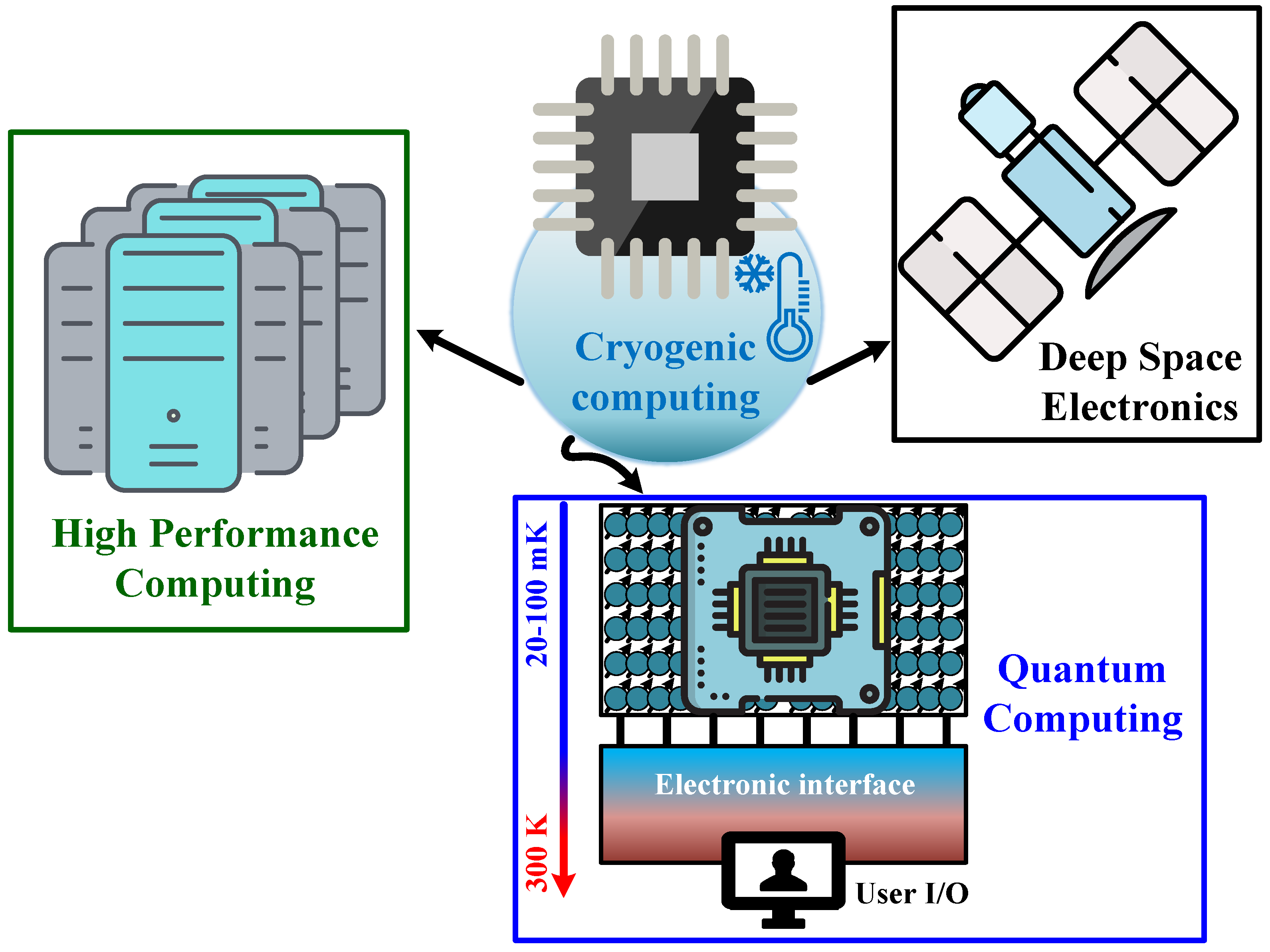
Figure 1. Cryogenic applications: from high-performance computing and deep space electronics, to quantum computing.
Electronics 11 00061 g001
Figure 2. Considered embedded memory technologies: (a) six-transistor static random-access memory (6T-SRAM), (b) two-transistor mixed gain cell nMOS-pMOS (2T NW-PR), and (c) perpendicular spin-transfer torque magnetic RAM (STT-MRAM) based on single barrier MTJ or double barrier MTJ.
Electronics 11 00061 g002
Figure 3. Statistical distributions of the SRAM hold, read, and write static noise margin (SNM) at (ac) 300 K and (df) 77 K. Simulations consider a nominal VDD = 1.2 V.
Electronics 11 00061 g003
Figure 4. Statistical distributions of the (a) read bitline voltages for ‘1’ ( V R B L ( 1 ) ) and ‘0’ ( V R B L ( 0 ) ) states at 77 K, and (b) its corresponding read voltage margin (VM) for 300 K and 77 K. Simulations consider a nominal VDD = 1.2 V.
Electronics 11 00061 g004
Figure 5. Storage node (SN) degradation for (a) 300 K and (b) 77 K. (c) Data retention time (DRT) statistical distribution at room and cryogenic temperatures. Simulations consider a nominal VDD = 1.2 V.
Electronics 11 00061 g005
Figure 6. Monte Carlo results under write access: statistical distribution of the pulse width (referred to the worst-case between AP→ P and P→ AP transitions) for SMTJ- and DMTJ-based STT-MRAM bitcells operating at (a,b) 300 K and (c,d) 77 K.
Electronics 11 00061 g006
Figure 7. Monte Carlo results under read access: statistical distribution of the bitline voltages for SMTJ- and DMTJ-based STT-MRAM bitcells operating at (a,b) 300 K and (c,d) 77 K.
Electronics 11 00061 g007
Table 1. Impact of cryogenic temperatures on different embedded memory technologies.
Impact of
Cryogenic Operation
Memory Technologies
SRAMGC-eDRAMSTT-MRAM
ProsLess leakage powerLess refresh powerBetter endurance
Faster memory access
(e.g., read/write)
Faster memory access
(e.g., read/write)
Better logic robustness
(e.g., higher TMR)
Less bitline resistanceLess bitline resistanceLess bitline resistance
Faster peripheral circuitryFaster peripheral circuitryFaster peripheral circuitry
ConsLower write SNMRefresh controller integration *Higher write energy
[*] It is referred as a disadvantage as compared to SRAM technology.
Table 2. SMTJ and DMTJ parameters.
DescriptionValue
MTJ diameter—d30 nm
Free layer thickness—tFL1.2 nm
SMTJ barrier thickness—tOX0.85 nm
DMTJ top barrier thickness—tOX,T0.85 nm
DMTJ bottom barrier thickness—tOX,B0.4 nm
Resistance-area product—RA11 Ω · μ m 2
Spin polarization factor—P0.66
Saturation magnetization—MS1.58 T
Gilbert damping factor— α 0.03
Interfacial perpendicular
Anisotropy constant—Ki
1.3 × 10 3   J /m2
Table 3. Figures of merit of different embedded memory technologies under a cryogenic temperature of 77 K and a nominal voltage of VDD = 1.2 V.
Parameter6T-SRAM2T Mixed GC
nMOS-pMOS
(2T NW-PR)
SMTJ-Based
STT-MRAM
DMTJ-Based
STT-MRAM
Normalized Area1X0.27X0.12X0.12X
Noise or Sensing
Margin * (mV)
(464/187/562)591244108
DRT (ms)Static23.3Non-VolatileNon-Volatile
Read time
(ns)
0.2520.2611
Write time
(ns)
0.1330.14419.43.28
Read
Energy/bit (fJ)
2.2790.73916.44.63
Write
Energy/bit (fJ)
2.4300.852969165
Refresh
Energy/bit (fJ)
1.591
Leakage
Power/bit † (fW)
376.26.768 ‡0
* Sensing margin is referred as the noise margins (HSNM/RSNM/WSNM), VM (at 4 μs), and VSM for the 6TSRAM, GC-eDRAM, and STT-MRAM configurations, respectively; † The values refer to the bitcell in standby mode; ‡ Average power from 0 to DRT. Refresh operation is neglected.
Publisher’s Note: MDPI stays neutral with regard to jurisdictional claims in published maps and institutional affiliations.