Abstract
A high-performance S-band down-conversion microstrip mixer, for operation from 77 K to 300 K, is described. The balanced mixer combines a 90 degree hybrid coupler, two Schottky diodes, a band pass filter, and a low pass filter. The coupler phase shift drastically improves noise rejection. The circuit was implemented according to the configuration obtained from extensive simulation results based on electromagnetic analysis. The experimental results agreed well with the simulation results, showing a maximum measured insertion loss of 0.4 dB at 2 GHz. The microstrip mixer can be easily adjusted to different frequency ranges, up to about 50 GHz, through the proper choice of microstrip configuration. This novel S-band cryogenic mixer, implemented without resorting to special components, shows a very high performance at liquid nitrogen temperatures, making this mixer very suitable for high-temperature superconductive applications, such as front-ends.
Keywords:
cryogenic mixers; down conversion; balanced mixer; hybrid coupler; BSF; LPF; microstrip; S-band 1. Introduction
Frequency converters are essential components in communication circuitry [1,2]. The most common approach to implementing these converters is the use of mixers. The characteristics of mixers vary according to their application. The performance of mixers is evaluated by parameters such as gain, noise, linearity, and power consumption. Up-converting filtering, minimal RF and Local Oscillator (LO) frequency leakage, bandwidth and conversion loss are important parameters that must be taken into account in the design of mixers [3,4,5,6,7,8,9].
A common configuration of frequency converters is the balanced mixer, consisting of two single-ended non-linear devices, combined with a hybrid junction [3]. Advanced technologies were introduced, improving the quality of balanced mixers. A high-performance mixer for broadcasting applications is the RF CMOS balanced mixer, in which the feedback signal improves its performance. This mixer employs a load-resonant LC network to increase gain and suppress high-order harmonic generation [10,11,12]. However, the short dynamic range of CMOS mixers limits the overall dynamic range of the receiver. Moreover, due to their nonlinearity, undesired harmonics, intermodulation terms and spurs are generated during frequency conversion. These may result in a lower signal-to-noise ratio, a lower receiver sensitivity, and a lower gain compression point [13].
A different approach for designing balanced mixers is based on hybrid microstrip transmission lines [14]. This design is frequently applied for high frequencies, Q-band and beyond [4,15]. Microstrip mixers can achieve high performance when combined with state-of-the-art planar filtering methods, such as dual-mode wideband bandpass filters (BPFs) [16,17,18], stepped impedance resonators [19], adjustable dual-band BPFs [20], dual-line coupling through controllable modal frequencies [21], and fractal geometry [22,23].
In order to transmit high-power signals with low losses and high frequency selectivity, the development of a specific, dedicated communication system is required. Cryogenic RF front-ends were demonstrated as frequency selective systems, with high stop band rejection and high effective signal-to-noise ratios [24,25,26]. High-performance cryogenic mixers are essential for these front-ends.
In this paper, we present the design of a down-conversion, S-band, microstrip balanced mixer. It incorporates a hybrid coupler, two high cut-off filters, and two wide frequency range Schottky diodes, with a low forward resistance at low temperatures. Based on extensive electromagnetic simulations, described in Section 3, we implemented a high-performance 2 GHz RF microstrip mixer, designed for use at room temperature as well as at cryogenic temperatures. We tested it with a LO frequency of 1.9 GHz, i.e., a down-conversion Intermediate Frequency (IF) of 100 MHz. The design, simulation, implementation, and experimental characterization of the microstrip mixer, both at room temperature and at 77 K, are described.
2. Balanced Mixer Structure
Several mixer configurations for RF communication are known. Examining the various options for the S-band, we chose to design a microstrip balanced mixer. In this type of mixer, the input noise that accompanies the LO signal, and thus may introduce noise in the intermediate frequency (IF), is highly reduced. The first component of the mixer, shown in Figure 1, is a hybrid coupler [3,27,28,29,30,31], which feeds into two diodes. We chose GaAs Schottky diodes (MGS903) because of their high cut-off frequency, high breakdown voltage, and low resistance at forward bias, even at low temperatures [32]. Room temperature simulations have shown similar performances for silicon and GaAs diodes. However, at 77 K GaAs, electron mobility is much higher than that of electrons in silicon and GaAs devices are known to perform extremely well at cryogenic temperatures. GaAs Schottky diodes feature a very short switching time, making them a perfect choice for RF applications, such as mixers, in the millimeter wave range.
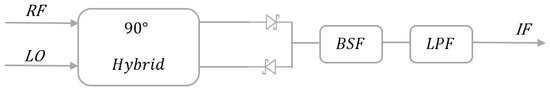
Figure 1.
Block diagram of the balanced mixer.
3. Simulations
3.1. Theory
We start the optimization process of the mixer by determining the initial width of the microstrip that is required to obtain a characteristic impedance of. For the microstrip structure presented in Figure 2, one can derive the ratio between the width W of the strip and the thickness h of the dielectric material by the following equation [3]:
where
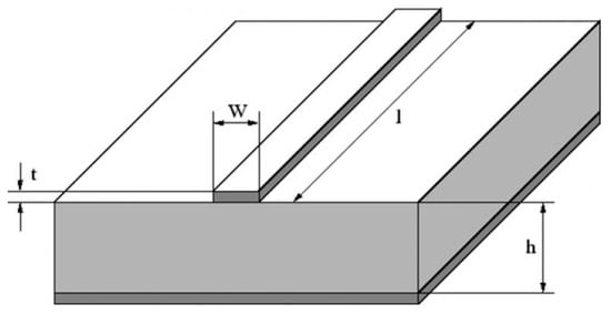
Figure 2.
MS line geometry. The strip width is W, and the dielectric substrate thickness is h.
Our dielectric substrate is a thick Rogers RT6002, with a relative dielectric constant and . For a Z0 = characteristic impedance; the derived values are and , i.e., .
Based on extensive simulations, we obtained different optimal widths of the strips leading to the various components, for impedance matching, which were slightly lower than the initial value. The results are presented in Table 1:

Table 1.
Optimal MS widths.
To derive the length of the quarter- and half-wavelength strips, we must determine the radiation wavelength in the strip. Since the radiation is not enclosed, some of the field lines are in the dielectric region and some are in air. This effect can be translated into an effective dielectric constant, which depends on the substrate dielectric constant, the substrate thickness, and the conductor width. The effective dielectric constant is given by [3]
Clearly, the effective dielectric constant is lower than the constant of the bulk material. For our parameters, we obtain:
from which we can derive the wavelength in the strip:
3.2. Simulation Results
Figure 3 shows the layout of the designed microstrip mixer. In order to reduce the system crosstalk, the RF and LO inputs are connected to the coupler with S-shaped half-wavelength transmission lines. The curved shaped inputs reduce possible mutual inductance between the ports. Using quarter-wavelength transmission lines, the two outputs of the coupler (red square) are connected to the two diodes (marked X in the red circle). The diode outputs are connected to the BSF (green rectangle) followed by the LPF (black rectangle). The bandwidth of the mixer is dependent on the bandwidth of the coupler and the filters. The filters feature a narrower bandwidth and are therefore more influential. The BSF was designed using the distributed elements filter method [3]. The stopband can be improved by increasing the order of the filter, but not without increasing the losses of the system. The LPF was designed using a radial stub pie configuration, where the stubs are the capacitive elements, and the distance between the stubs is the inductance element. Hence, by changing the radius and distance of stubs, the bandwidth of the mixer can be determined. Accordingly, the filters were designed taking into account the current distribution at the critical frequencies [33]. The via connected to the coupling port of the coupler serves as an RF choke (RFC). The other vias serve to attach the system to the package to increase its mechanical strength.
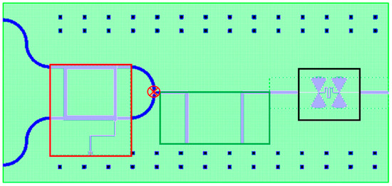
Figure 3.
Layout of designed microstrip mixer: coupler—red rectangle; two diodes—red circled X; BSF—green rectangle; LPF—black rectangle.
The performance of the designed microstrip mixer can be analyzed based on lumped components equivalent circuit extracted by methods described in references [16] and [34], and transmission lines model described in [35]. We chose to analyze the microstrip mixer using the AWR microwave circuit design software. The AWR uses Maxwell equations to numerically compute the frequency response of the circuit from its physical parameters. The AWR makes it possible to perform accurate analysis using linear and nonlinear harmonic balance, nonlinear Volterra-series, electromagnetic, and spectra simulation, and features real-time tuning and optimizing capabilities. There are several requirements for an ideal mixer: the RF and LO inputs must be interchangeable, a 50 Ω input impedance for both ports, and a high attenuation between the input ports and the output (S31, S32) is essential. The final configuration of the mixer was derived through the optimization of the dimensions of the microstrips and the distance between them. The simulation results are detailed in Appendix A, showing the effects of MS width on the performance of the filters and the mixer. The optimal results are presented in Figure 4, showing that the designed coupler conforms with these requirements. The simulations showed that the power conversion losses were 12 dB and the RF-LO isolation was around 0.5 dB. This is a well-known trade-off in balanced mixers based on 90 degrees hybrid couplers, with high input matching (S11) and low isolation [3]. Full electronic circuit AWR emp software files are provided in the Supplementary Materials.
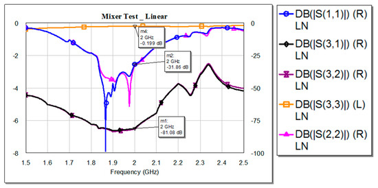
Figure 4.
Simulation results for S parameters of the mixer.
4. Room Temperature Experimental Results
The microstrip mixer, presented in Figure 5, was produced based on the simulations and optimization. The dimensions of the entire system are 209 × 108 mm2. The circuit is implemented on a 508 μm thick RT6002 dielectric substrate. Since the substrate dielectric material is thin, two measures were taken to protect the circuit. A layer of tin that was deposited on top of the copper wiring, and the mixer was packed in 5 mm thick aluminum, which facilitated connection to the SMA connectors.
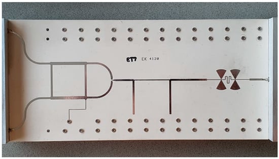
Figure 5.
Photograph of the produced microstrip mixer.
We measured the S parameters as a function of frequency, using a vector network analyzer (VNA). The results are presented in Figure 6. The experimental results, measured at room temperature, were very similar to the theoretical results obtained by simulations (Figure 4). S33 was slightly different, indicating that the impedance matching in port 3 was not high enough. The experimental results agreed well with the simulation results, showing a maximum measured insertion loss of 0.4 dB at 2 GHz.
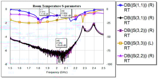
Figure 6.
S parameters measured at room temperature.
In addition to the S parameters, we measured three parameters using a spectrum analyzer (SA) to evaluate the performance of the mixer. The IF output signal as function of frequency is presented in Figure 7. The filtering of the RF signal to the IF output is shown in Figure 8. The LO leakage to the IF output is presented in Figure 9.
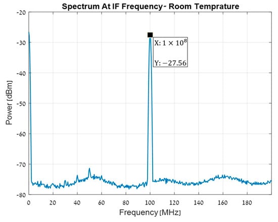
Figure 7.
Mixer output IF signal at room temperature.
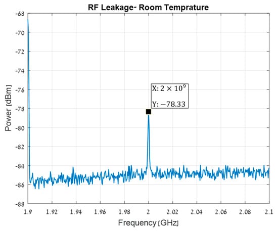
Figure 8.
RF leakage to the output port measured at room temperature.
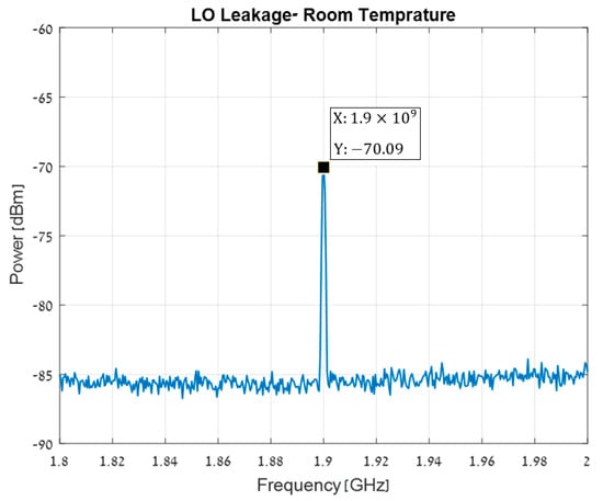
Figure 9.
LO leakage to the output measured at room temperature.
The leakage of the RF frequency to the output is shown in Figure 8. The IF leakage is −78.33 dBc, a clear indication of the high RF-IF isolation. The RF input power is −20 dBm at 2 GHz, the LO input power is 7 dBm at 1.9 GHz, and the output power for the IF is PIF = −27.56 dBm at 100 MHz. The mixer Conversion Loss is therefore , where is the RF cable loss. Figure 9 shows the LO leakage to the output. The high LO-IF isolation is expressed by the very low LO leakage, of around −70.09 dBc.
5. Experimental Results at 77 K
We tested the performance of the circuit at liquid nitrogen temperature (77 K). The various S parameters, measured as a function of frequency with VNA, are shown in Figure 10. These measured parameters are similar to those derived from simulations and those measured at room temperature. Even though the mixer was designed based on room temperature parameters, it performed very well at cryogenic temperatures. The resistance at forward bias of the GaAs Schottky diodes was low, as required. The cryogenic measurement setup is described in Appendix B.
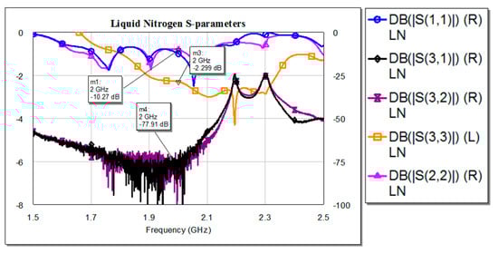
Figure 10.
S parameters measured at liquid nitrogen temperature.
The output power of the IF, measured with SA at 77 K, is shown in Figure 11. The measured power at 100 MHz is PIF = −30.94 dBm. This output is obtained for an RF input power of −20 dBm at 2 GHz, and a LO input power of 7 dBm at 1.9 GHz. Therefore, the mixer Conversion Loss is , where is the RF cable loss.
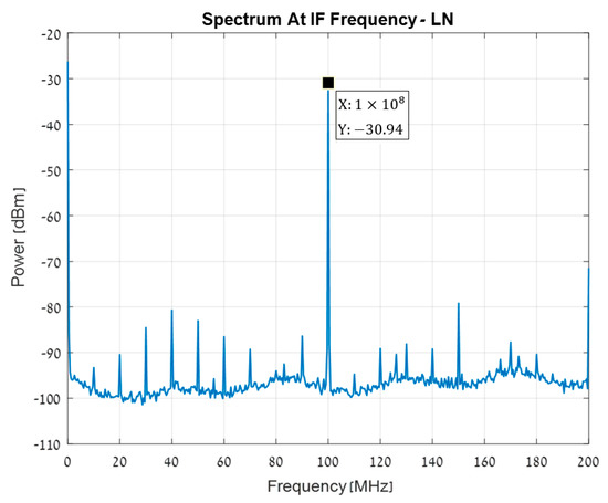
Figure 11.
Mixer output: IF signal measured at liquid nitrogen temperature.
The measured up-converting rejection is shown in Figure 12. At the sum of the LO and RF frequencies, 3.9 GHz, P = −86.71 dBm and at the second harmony of the LO signal, 3.8 GHz, P = −57.02 dBm, i.e., the high frequency filtering is very effective.
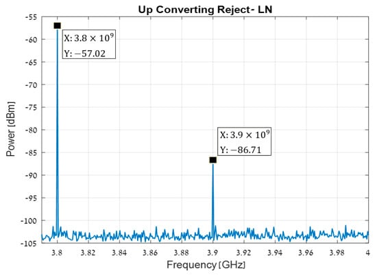
Figure 12.
Up conversion reject measured at liquid nitrogen temperature.
The leakage of the input signals to the IF output is shown in Figure 13. The RF-to-IF leakage is −88.74 dBc and LO-to-IF leakage is −69.65 dBc.
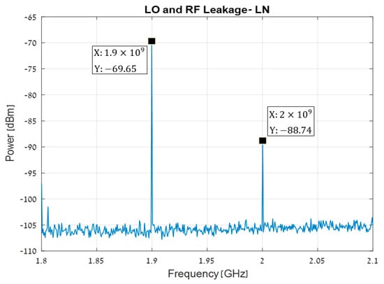
Figure 13.
LO and RF leakage measured at liquid nitrogen temperature.
The high performance of the mixer at liquid nitrogen temperature makes this configuration attractive for cryogenic use, such as for circuits implemented in superconductors [36,37,38,39,40].
6. Discussion
There is a limited number of reported mixers for the S-band at cryogenic temperatures. In the following table we compare the performance of different mixers for cryogenic use, along with typical data for mixers intended for room temperature operation. There are several parameters that influence the performance of mixers, such as up-converting filtering, minimal RF and LO frequency leakage, bandwidth, and conversion loss [3,4,5,6,7,8,9]. Due to the trade-offs between these design metrics, it is difficult to determine unequivocally the quality of mixers.
Table 2 demonstrates clearly the results of the proper selection of the mixer configuration, and the optimization process for every one of its components. Even though we chose the IF and LO frequencies to differ by 100 MHz only, one can discern the high performance of our mixer relative to other mixers reported in scientific and industrial research in almost every parameter, both in the cryogenic and room temperature ranges.
Table 2.
RF mixers data table at cryogenic and room temperatures.
7. Conclusions
We designed and manufactured a full down-conversion mixer, based on a 90° hybrid coupler. The final configuration of the mixer was derived following several optimization steps based on extensive simulations. The inputs to the coupler were selected as S-shape microstrip, to reduce mutual inductance. The optimal dimensions of the strips were determined by the simulation results. The frequency conversion was based on a pair of GaA Schottky diodes, connected to the coupler by microstrips implemented according to the simulation optimizations. The output of the convertor is connected to a BSF, for which the distributed elements filter method was selected. The final element is a LPF, designed using a radial stub pie configuration. Since the stubs are the capacitive elements, and the distance between the stubs is the inductance element, one can select the bandwidth by properly selecting the radius and distance of the stubs.
The scattering coefficients of the system, along with the other parameters of the mixer, were measured and compared with the results of the simulations based on the electromagnetic analysis. The mixer was tested both at room temperature and at a liquid nitrogen temperature of 77 K. The experimental results agreed well with the simulations at both temperatures.
This proposed mixer is an excellent solution for improving communication in crowded areas where reception is weak. Moreover, the high performance at liquid nitrogen temperature makes this configuration very attractive for cryogenic use, such as for circuits implemented in high critical temperature superconductors.
The mixer can be easily adjusted to other frequencies, up to about 50 GHz, by proper choice of the length of the transmission lines.
Supplementary Materials
The electronic circuit AWR emp software file is available online at https://www.mdpi.com/article/10.3390/electronics11010102/s1.
Author Contributions
Conceptualization, N.C., O.S. and E.H.; methodology, N.C., O.S. and E.H.; software, N.C.; validation, S.E.S., O.S. and E.H.; investigation, N.C., O.S. and E.H.; writing—original draft preparation, N.C., S.E.S. and E.H.; writing—review and editing, S.E.S. and E.H.; experiments were performed by, N.C., O.S. and E.H.; supervision, O.S., E.H. and E.F.; funding acquisition, E.F. All authors have read and agreed to the published version of the manuscript.
Funding
This research received no external funding.
Institutional Review Board Statement
Not applicable.
Informed Consent Statement
Not applicable.
Data Availability Statement
The data presented in this study are available on request from Dr. Holdengreber.
Conflicts of Interest
The authors declare no conflict of interest.
Appendix A
The results of the simulations are presented below, showing the effects of the width of the MS lines on the performance of the filters and the overall performance of the mixer. The main task of the filters is to reject the large LO signal. As can be seen from Figure A1a,b, both a very sharp notch in the simulations of insertion loss and a flat high return loss were obtained for the LO frequency, with the best response (symmetric and without ripples) for the optimal dimension of the BSF line (W = 1.28 mm).
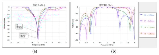
Figure A1.
BSF IL, S21 (a) and RL, S11 (b) vs. frequency for various MS widths.
Figure A2a,b shows the simulation results for the LPF. Clearly, at the low frequency range, the transmission is maximal and the reflection minimal, as expected, with the lowest reflection at the optimal dimensions, along with a sharp roll-off.
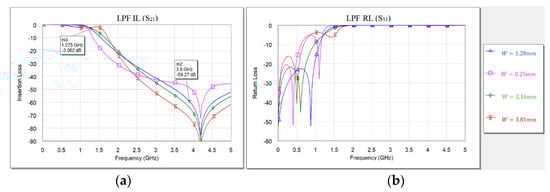
Figure A2.
LPF S21 (a) and S11 (b) vs. frequency for various MS widths.
The simulations of the coupler performance, presented in Figure A3a,b, show clearly that minimal changes in line width resulted in increased impedance mismatch, and, as a result, lower reflection losses than those obtained at the optimal dimensions (1.27 nm).
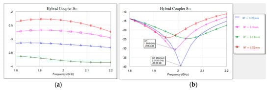
Figure A3.
Hybrid coupler scattering coefficients, S31 (a) and S11 (b) vs. frequency for various MS widths.
Appendix B
The cryogenic measurement system is illustrated in Figure A4. The system is composed of three main elements: a VNA, a computing system, and a polystyrene liquid nitrogen container [46,47,48]. The S-parameters were measured using the VNA, while the Device Under Test (DUT) was immersed in liquid nitrogen. The VNA was calibrated using a standard calibration procedure through a connection and three loads: open (high impedance), short, and 50 Ohms (matched), eliminating the effects of all the components apart from the DUT from the measured data. The calibration was performed separately for 300 K measurements and 77 K measurements. Since the VNA features two inputs and the device features three ports, several measurements are required to obtain all the S-parameters. While testing the scattering coefficients of two out of three ports, the other was connected to a matching impedance, a 50 Ohm load.
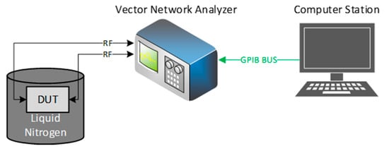
Figure A4.
Illustration of the s-parameters measurement setup.
For the conversion loss, leakage, and isolation measurements, the RF and LO ports were fed using a signal generator, while the IF port was measured using a spectrum analyzer (Figure A5). For the cryogenic measurements, the DUT was immersed in the same polystyrene container depicted in Figure A4. The RF cables used in the two setups were rigid coaxial cables with male SMA connectors at both ends. They were immersed in the liquid nitrogen with the DUT.
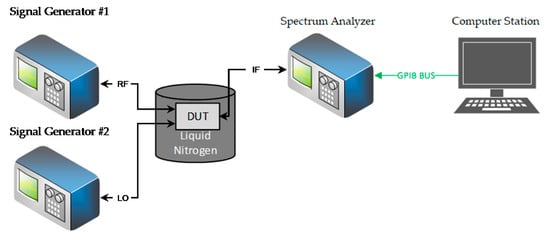
Figure A5.
Illustration of the conversion loss measurement setup.
References
- Algumaei, M.Y.; Shairi, N.A.; Zakaria, Z.; Ibrahim, I.M. Review of Mixer and Balun Designs for UWB Applications. Int. J. Appl. Eng. Res. 2017, 12, 6514–6522. [Google Scholar]
- Vasjanov, A.; Barzdenas, V. A Methodology Improving Off-Chip, Lumped RF Impedance Matching Network Response Accuracy. Electronics 2018, 7, 188. [Google Scholar] [CrossRef] [Green Version]
- Pozar, M.D. Microwave Engineering, 4th ed.; Wiley: Hoboken, NJ, USA, 2011; pp. 147–149, 272, 625–627, 646–649, 654. [Google Scholar]
- Ji, D.; Zhang, B.; Yang, Y.; Niu, Z.; Yong, F.; Chen, X. A 220-GHz Third-Harmonic Mixer Based on Balanced Structure and Hybrid Transmission Line. IEEE Access 2019, 7, 50007–50011. [Google Scholar] [CrossRef]
- Mahmou, R.K.; Faitah, K. Designing of RF Single Balanced Mixer with a 65nm CMOS Technology Dedicated to Low Power Consumption Wireless Applications. IJCSI Int. J. Comput. Sci. Issues 2012, 9, 358–363. [Google Scholar]
- Na, D.; Kim, T.W. A 1.2 V, 0.87–3.7 GHz Wideband Low-Noise Mixer Using a Current Mirror for Multiband Application. IEEE Microw. Wirel. Compon. Lett. 2012, 22, 91–93. [Google Scholar] [CrossRef]
- Bai, D.D.; Du, J.; He, Y.S. Characterizations of High-Temperature Superconducting Step-Edge Josephson Junction Mixer. IEEE Trans. Appl. Supercond. 2014, 24, 1501404. [Google Scholar]
- Mohsenpour, M.; Saavedra, C.E. Method to Improve the Linearity of Active Commutating Mixers Using Dynamic Current Injection. IEEE Trans. Microw. Theory Tech. 2016, 64, 4624–4631. [Google Scholar] [CrossRef]
- Kumar, S.; Saraiyan, S.; Dubey, S.K.; Pal, S.; Islam, A. A 2.4 GHz double balanced downconversion mixer with improved conversion gain in 180-nm technology. Microsyst. Technol. 2020, 26, 1721–1731. [Google Scholar] [CrossRef]
- Xiangning, F.; Chisheng, Z.; Lei, Z. A 2.4 GHz RF CMOS up-conversion mixer for wireless sensor networks nodes. In Proceedings of the 2009 International Conference on Wireless Communications & Signal Processing, Nanjing, China, 13–15 November 2009; pp. 1–5. [Google Scholar]
- Oh, H.; Kim, J.; Lim, J.; Kim, C. A 2.4-GHz High Conversion Gain Passive Mixer Using Q-Boosted π-Type LCL Matching Networks in 90-nm CMOS. IEEE Microw. Wirel. Compon. Lett. 2017, 27, 736–738. [Google Scholar] [CrossRef]
- Kalamani, C. Design of Differential LNA and Double Balanced Mixer using 180 nm CMOS Technology. Microprocess. Microsyst. 2019, 71, 102850. [Google Scholar] [CrossRef]
- Kashani, M.H.; Asghari, M.; Yavari, M.; Mirabbasi, S. A +7.6 dBm IIP3 2.4-GHz Double-Balanced Mixer With 10.5 dB NF in 65-nm CMOS. IEEE Trans. Circuits Syst. II Express Briefs 2021, 68, 3214–3218. [Google Scholar] [CrossRef]
- Feng, W.; Che, W.; Xue, Q. The Proper Balance: Overview of Microstrip Wideband Balance Circuits with Wideband Common Mode Suppression. IEEE Microw. Mag. 2015, 16, 55–68. [Google Scholar] [CrossRef]
- Shi, X.; Zhu, X. Design of Balanced Mixer with 180 Degrees Hybrid Network Based on Cruciform Coupler. In Proceedings of the 2018 11th UK-Europe-China Workshop on Millimeter Waves and Terahertz Technologies (UCMMT), HangZhou, China, 5–7 September 2018; pp. 1–3. [Google Scholar]
- Lalbakhsh, A.; Alizadeh, S.M.; Ghaderi, A.; Golestanifar, A.; Mohamadzade, B.; Jamshidi, M.; Mandal, K.; Mohyuddin, W. A Design of a Dual-Band Bandpass Filter Based on Modal Analysis for Modern Communication Systems. Electronics 2020, 9, 1770. [Google Scholar] [CrossRef]
- Ahmadi, A.; Makki, S.V.; Lalbakhsh, A.; Majidifar, S. A Novel Dual-Mode Wideband Band Pass Filter. Appl. Comput. Electromagn. Soc. J. 2014, 29, 735–742. [Google Scholar]
- Lalbakhsh, A.; Jamshidi, M.; Siahkamari, H.; Ghaderi, A.; Golestanifar, A.; Richard, L.; Talla, J.; Simorangkir, R.B.V.B.; Mandal, K. A compact lowpass filter for satellite communication systems based on transfer function analysis. Int. J. Electron. Commun. 2020, 124, 153318. [Google Scholar] [CrossRef]
- Dehghani, K.; Karimi, G.; Lalbakhsh, A.; Maki, S.V. Design of lowpass filter using novel steppedimpedance resonator. Electron. Lett. 2014, 50, 37–39. [Google Scholar] [CrossRef]
- Lalbakhsh, A.; Ghaderi, A.; Mohyuddin, W.; Simorangkir, R.B.V.B.; Bayat-Makou, N.; Ahmad, M.S.; Lee, G.H.; Kim, K.W. A Compact C-Band Bandpass Filter with an Adjustable Dual-Band Suitable for Satellite Communication Systems. Electronics 2020, 9, 1088. [Google Scholar] [CrossRef]
- Lalbakhsh, A.; Karimi, G.; Sabaghi, F. Triple mode spiral wideband bandpass filter using symmetric dual-line coupling. Electron. Lett. 2017, 53, 795–797. [Google Scholar] [CrossRef]
- Lalbakhsh, A.; Lotfi, A.; Naser-Moghadasi, M. Microstrip Hairpin Bandpass Filter Using Modified Minkowski Fractal-Shape for Suppression of Second Harmonic. IEICE Trans. Electron. 2012, 95, 378–381. [Google Scholar] [CrossRef]
- Lotfi, A.; Lalbakhsh, A. Improved microstrip hairpin-line bandpass filters for spurious response suppression. Electron. Lett. 2012, 48, 858–859. [Google Scholar] [CrossRef]
- Markiewicz, T.G.; Wesołowski, K.W. Cryogenic Cooling in Wireless Communications. Entropy 2019, 21, 832. [Google Scholar] [CrossRef] [Green Version]
- Narahashi, S.; Satoh, K.; Kawai, K.; Koizumi, D. Cryogenic Receiver Front-End for Mobile Base Stations. In Proceedings of the 2008 China-Japan Joint Microwave Conference, Shanghai, China, 10–12 September 2008; pp. 619–622. [Google Scholar]
- Gawande, R.; Bradley, R.; Langston, G. Low noise, 0.4–3 GHz cryogenic receiver for radio astronomy. Rev. Sci. Instrum. 2014, 85, 104710. [Google Scholar] [CrossRef] [PubMed]
- Holdengreber, E.; Mizrahi, M.; Glassner, E.; Koral, Y.; Schacham, S.; Farber, E. Phase shift combiner for multi-channel VHF communication. Int. J. Microw. Wirel. Technol. 2017, 9, 79–83. [Google Scholar] [CrossRef]
- Holdengreber, E.; Mizrahi, M.; Farber, E. Quasi-dynamical multi-channel coupler based on high temperature superconducting films. In Proceedings of the IEEE 27th Convention of Electrical and Electronics Engineers in Israel, Eilat, Israel, 14–17 November 2012; pp. 1–4. [Google Scholar]
- Mizrahi, M.; Glassner, E.; Bachar, N.; Farber, E.; Abramovich, A.; Koral, Y. VHF multi-channel coupler for RF communication. In Proceedings of the 2009 IEEE International Conference on Microwaves, Communications, Antennas and Electronics Systems, Tel Aviv, Israel, 9–11 September 2009. [Google Scholar]
- Lalbakhsh, A.; Mohamadpour, G.; Roshani, S.; Ami, M.; Roshani, S.; Sayem AS, M.; Koziel, S. Design of a Compact Planar Transmission Line for Miniaturized Rat-Race Coupler with Harmonics Suppression. IEEE Access 2021, 9, 129207–129217. [Google Scholar] [CrossRef]
- Abdipour, A.; Honari, M.M.; Mousavi, P.; Mirzavand, R. Class of miniaturised/arbitrary power division ratio couplers with improved design flexibility. IET Microw. Antennas Propag. 2015, 9, 1066–1073. [Google Scholar]
- MACOM. United States. Available online: https://www.macom.com/products/product-detail/MGS903 (accessed on 1 September 2021).
- Hu, S.; Hu, Y.; Zheng, H.; Zhu, W.; Gao, Y.; Zhang, X. A Compact 3.3–3.5 GHz Filter Based on Modified Composite Right-/Left-Handed Resonator Units. Electronics 2020, 9, 427. [Google Scholar] [CrossRef] [Green Version]
- Karimi, G.; Lalbakhsh, A.; Dehghani, K.; Siahkamari, H. Analysis of Novel Approach to Design of Ultra-wide Stopband Microstrip Low-Pass Filter Using Modified U-Shaped Resonator. Etri J. 2015, 37, 945–950. [Google Scholar] [CrossRef]
- Karimi, G.; Amirian, M.; Lalbakhsh, A.; Ranjbar, M. A new microstrip coupling system for realization of a differential dual-band bandpass filter. Int. J. Electron. Commun. 2019, 99, 186–192. [Google Scholar] [CrossRef]
- Huhtinen, H.; Ulriksson, J.; Malmivirta, M.; Järvinen, J.; Jha, R.; Awana, V.P.S.; Vasiliev, S.; Paturi, P. Deposition of YBCO Thin Films in View of Microwave Applications. IEEE Trans. Appl. Supercond. 2017, 27, 1–5. [Google Scholar] [CrossRef]
- Holdengreber, E.; Moshe, A.G.; Mizrahi, M.; Khavkin, V.; Schacham, S.E.; Farber, E. High sensitivity high Tc superconducting Josephson junction antenna for 200 GHz detection. J. Electromagnet. Wave. 2019, 33, 193–203. [Google Scholar] [CrossRef]
- Holdengreber, E.; Moshe, A.G.; Vigneswaran, D.; Schacham, S.E.; Farber, E. Temperature Effect on Selectivity of HTSC Josephson Junction Detector. IEEE Trans. Appl. Supercond. 2021, 31, 1102004. [Google Scholar] [CrossRef]
- Holdengreber, E.; Schacham, E.; Farber, E. Impedance mismatch elimination for improved THz detection by superconducting Josephson junctions. In Proceedings of the Antennas and Propagation Conference 2019 (APC-2019), Birmingham, UK, 11–12 November 2019; pp. 1–3. [Google Scholar]
- Holdengreber, E.; Gao, X.; Mizrahi, M.; Schacham, S.E.; Farber, E. Superior impedance matching of THz antennas with HTSC josephson junctions. Supercond. Sci. Technol. 2019, 32, 074006. [Google Scholar] [CrossRef]
- Romanofsky, R.R. An X-Band Mixer Engineered for 77-K Operation; National Aeronautics and Space Administration, Office of Management, Scientific and Technical Information Program: Washington, DC, USA, 1995. [Google Scholar]
- Watkins-Johnson. United States. Available online: https://www.abex.co.uk/esales/microwave/magnum_microwave/mixer/mo74p-2/000/index.php (accessed on 21 September 2021).
- Nguyen, N.T.P.; Van Tran, S.; Nguyen, D.B.; Mai, L. Design and implement a single balanced mixer at S band. In Proceedings of the 2015 International Conference on Advanced Technologies for Communications (ATC), Nha Trang, Vietnam, 14–16 October 2015; pp. 637–641. [Google Scholar]
- Sudow, M.; Andersson, K.; Nilsson, P.; Rorsman, N. A highly linear double balanced Schottky diode S-band mixer. IEEE Microw. Wirel. Compon. Lett. 2006, 16, 336–338. [Google Scholar] [CrossRef]
- Zhang, T.; Du, J.; Guo, Y.J. An 8–10-GHz Low-Loss Image-Reject HTS Mixer Based on Cascaded Josephson Junctions. IEEE Microw. Wirel. Compon. Lett. 2021, 31, 945–948. [Google Scholar] [CrossRef]
- Holdengreber, E.; Mizrahi, M.; Glassner, E.; Dahan, Y.; Castro, H.; Farber, E. Design and implementation of an RF coupler based on YBCO superconducting films. IEEE Trans. Appl. Supercond. 2015, 25, 1500905. [Google Scholar] [CrossRef]
- Dahan, Y.; Holdengreber, E.; Mizrahi, M.; Schacham, S.E.; Farber, E. Multichannel Transmitting System Based on High Temperature Superconducting Phase Shifter. IEEE Trans. Appl. Supercond. 2020, 30, 3500506. [Google Scholar] [CrossRef]
- Dahan, Y.; Holdengreber, E.; Glassner, E.; Sorkin, O.; Schacham, S.E.; Farber, E. Measurement of Electrical Properties of Superconducting YBCO Thin Films in the VHF Range. Materials 2021, 14, 3360. [Google Scholar] [CrossRef]
Publisher’s Note: MDPI stays neutral with regard to jurisdictional claims in published maps and institutional affiliations. |
© 2021 by the authors. Licensee MDPI, Basel, Switzerland. This article is an open access article distributed under the terms and conditions of the Creative Commons Attribution (CC BY) license (https://creativecommons.org/licenses/by/4.0/).