Abstract
Fully differential amplifiers require the use of common-mode feedback (CMFB) circuits to properly set the amplifier’s operating point. Due to scaling trends in CMOS technology, modern amplifiers increasingly rely on cascading more than two stages to achieve sufficient gain. With multiple gain stages, different topologies for implementing CMFB are possible, whether using a single CMFB loop or multiple ones. However, the impact on performance of each CMFB approach has seldom been studied in the literature. The aim of this work is to guide the choice of the CMFB implementation topology evaluating performance in terms of stability, linearity, noise and common-mode rejection. We present a detailed theoretical analysis, comparing the relative performance of two CMFB configurations for 3-stage OTA topologies in an implementation-agnostic manner. Our analysis is then corroborated through a case study with full simulation results comparing the two topologies at the transistor level and confirming the theoretical intuition. An active-RC filter is used as an example of a high-linearity OTA application, highlighting a 6 dB improvement in in the multi-loop implementation with respect to the single-loop case.
1. Introduction
The Operational Transconductance Amplifier (OTA) is a fundamental building block in analog circuit design. It is designed to provide large voltage gain and to drive only capacitive loads, so it is characterized by a large output impedance [1]. The circuit symbol of the OTA is shown in Figure 1. In many applications (such as active filters), the OTA has a negative feedback configuration applied to it, which improves the circuit’s bandwidth and linearity, reduces noise and sensitivity to process variations [1]. However, those benefits rely on the OTA having high gain. The higher the OTA’s gain, the better the accuracy and the rejection of unwanted noise.
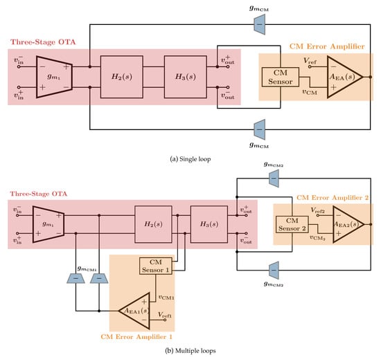
Figure 1.
Possible common-mode feedback (CMFB) implementations for a 3-stage amplifier. The blocks labeled H2(s) and H3(s) together constitute the inner amplifier, including its compensation network.
As supply voltages continue to scale down in newer process technologies, achieving a high gain with a simple two-stage OTA becomes more difficult and using the traditional cascode configuration severely limits signal excursion. One solution to this problem is to use multiple gain stages in cascade [2,3]. Moreover, high-precision applications necessitate the use of a fully-differential multi-stage OTA for the rejection of even-order harmonic distortion and common-mode noise, which provide the added benefit of improving dynamic range.
While differential signaling leads to improved linearity, it adds complexity to the circuit by requiring the use of a common-mode feedback (CMFB) loop to set the amplifier’s DC operating point and reject common-mode disturbances. The design of CMFB loops, therefore, forms an integral part of many applications and a careful approach is needed to ensure they remain stable while being fast enough to reject common-mode disturbances that lie within the OTA’s operational bandwidth [1,4].
An extra complication to the CMFB design problem in multi-stage OTAs is that there are many different topological approaches to the implementation. For the three-stage amplifier case, there are at least two different approaches as shown in Figure 1.
As shown in Figure 1a, one possible solution is to have a single CMFB loop sensing the output common-mode voltage and feeding back a common-mode current into the output of the first stage. In the CMFB loop, a common-mode (CM) sensor is used to sense the common-mode component of two voltages and then a CM error amplifier amplifies the difference between this common-mode component and the reference voltage that we desire to set the CM component to. Thus, the CM negative feedback loop sets the common-mode component of the voltages sensed by the CM sensor to the reference voltage input to the CM error amplifier.
Another solution, shown in Figure 1b, is to use two CMFB loops, one to set the output common-mode voltage by feeding back current into the output nodes and one to set the output common-mode voltage of the stage and feeds back common-mode current into the output of the first stage.
In the multi-stage amplifier literature, the topic of fully-differential OTA design is rarely broached, in particular when it comes to the design trade-offs of different CMFB approaches. If the intermediate gain stage is implemented in a fully-differential fashion, several options for the CMFB loop implementation are available, such as using a single loop that does not include all three stages [5] or using one loop per stage [6]. Such options are not available for high-linearity applications since in those cases, a pseudo-differential intermediate stage is used to improve signal swing and reduce distortion. The authors of [7] implemented a two-loop switched-capacitor solution but do not go into details concerning the trade-offs involved in the design of those CMFB loops. Some authors have even achieved the impressive feat of designing four-stage fully differential amplifiers with a single CMFB loop [4,8], but their approaches rely on the common-mode error amplifier pole being at a much higher frequency than the differential loop bandwidth, which may not be feasible in low-power amplifiers or high-frequency applications. Additionally, neither work considers the impact of the CMFB loop design on amplifier linearity.
There is therefore a real need to approach these trade-offs in a systematic manner that offers intuition to designers on the relative merits of different CMFB topologies. This is the aim of this work.
At first glance, it seems that using multiple loops unnecessarily increases complexity and power consumption, leading to the conclusion that the single-loop option is the better solution. However, in this work we propose to investigate whether this original intuition is justified. The performance of the two solutions will be qualitatively compared using different metrics of performance. Among our findings, it is shown that using a single loop can be challenging in terms of ensuring its stability and may end up being a worse option in terms of linearity, area and power consumption.
Our analysis, both theoretical and with transistor-level simulations, proves the counter-intuitive result that using multiple loops is actually better for performance, especially in terms of linearity—arguably the most important metric that leads to the adoption of fully-differential circuits in the first place.
This paper is organized as follows—in Section 2, an extensive theoretical analysis of the two solutions is developed, based on the aspects of stability, linearity, noise performance and common-mode rejection (CMR). In Section 3, a case study that implements both solutions at the transistor level is simulated to confirm the results of the analysis. Particular care is taken to ensure that both implementations consume the same amount of power and share the same circuit architecture (except the CMFB loops) to ensure a fair comparison. Also, an active-RC biquad low-pass filter is implemented, highlighting the linearity design trade-off in a common application of multi-stage amplifiers. Section 4 provides a summary discussion of the merits of each implementation. Finally, some conclusions are given.
2. Theoretical Comparison
In this section, the different performance aspects of the two designs are compared theoretically, with transistor-level simulation results confirming the analysis in the next section.
2.1. Stability
Since there are many different approaches to compensating the differential-mode loop of a three-stage amplifier, it is important to evaluate the stability of the different CMFB approaches in a manner that is agnostic to the underlying compensation scheme. For this reason, we make use of the rate of closure (ROC) concept [9] to make qualitative arguments about stability. In the transistor-level case study, the more traditional metrics of phase margin (PM) and settling time are used.
For a negative feedback loop composed of two factors , the ROC can be obtained by plotting the magnitudes of and on the same set of axes. The point of intersection of the two plots will be the unity-gain frequency of the loop and the ROC is the absolute value of the difference between the slopes of the two curves at that point (measured in dB/decade). The PM can then be approximated by
The only limitation on the use of the ROC approach is that ROC correlates to PM only for minimum-phase systems, which means that any amplifiers whose transfer functions contain right-half plane (RHP) zeros cannot be studied using this approach. However, given their negative effects on stability, RHP zeros are usually avoided in the majority of amplifiers [3,10,11].
It should be noted that, although ROC curves are most commonly used to express negative feedback loops in terms of the feedforward factor and the feedback factor , the same principle applies for any factorization of the loop gain and the forthcoming discussion, in fact, relies on a different factorization—the CM loop gain is expressed as the product of the differential-mode gain and an algebraic factor that does not correspond to physical circuit blocks.
2.1.1. Single Loop
Figure 2 shows the CM equivalent small-signal circuit model for the single-loop case. In the figure, it is assumed that the transfer function of the CM voltage sensor is absorbed into . It is further assumed that includes the loading effect of the compensation network used inside the inner amplifier’s stages, for which the transfer function is given by .
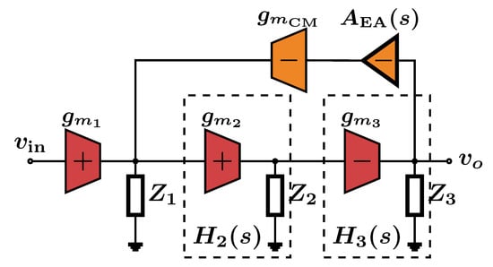
Figure 2.
Small-signal model of the common-mode (CM) equivalent circuit for the single-loop design.
As a bare minimum, the transfer function has one pole and may be modeled by
and this leads to the following formula for the loop gain of the CMFB loop:
where denotes the differential-mode gain, a third-order transfer function since the differential path has 3 stages. Since contains at least one pole, the CMFB loop gain will be at least of the fourth order.
To study the ROC, we plot the magnitudes of and on the same curve and their point of intersection represents the crossover frequency. This is depicted in Figure 3.
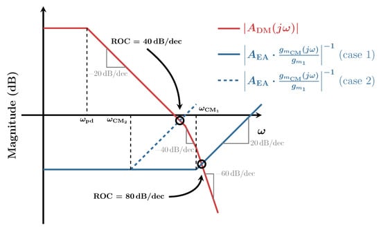
Figure 3.
Rate of closure (ROC) curves for the single-loop design.
As seen in the figure, the worst-case ROC is 80 dB/decade, indicating a negative PM. The PM can be improved by slowing down the CM error amplifier as demonstrated by the dashed curve. This second case exhibits an ROC of 40 dB/decade which indicates a zero PM (marginal stability). The phase margin can be improved to about 45° by aiming for a ROC of 20 dB/decade, but the plot of Figure 3 indicates that achieving this ROC requires slowing down the CM loop considerably, which can only be achieved in an efficient manner by using compensation.
The suggested compensation scheme for this case is shown in Figure 4—adding a compensation capacitor with a buffer. This results in the CM amplifier’s pole () being defined primarily by the compensation capacitor instead of a much smaller parasitic element. The buffer is added to isolate the differential mode loop and prevent the compensation capacitor from loading it. Note that selecting the output of for compensation, takes advantage of the Miller effect to allow the use of a smaller physical capacitor compared to using the input of .
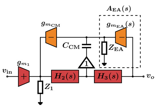
Figure 4.
Small-signal model of the CM equivalent circuit for the compensated single-loop design.
In this case, the CM loop gain is given by
where
showing the reduction in the CMFB error amplifier bandwidth due to the loading by the compensation capacitor. We can thus write
As noted above, an ROC of about 20 dB/decade can be achieved by reducing the bandwidth of the CMFB error amplifier. To quantify this reduction in bandwidth, we find the critical point at which the ROC changes from 40 dB/decade to 20 dB/decade. This is illustrated in Figure 5 where denotes the dominant pole of the differential-mode loop.
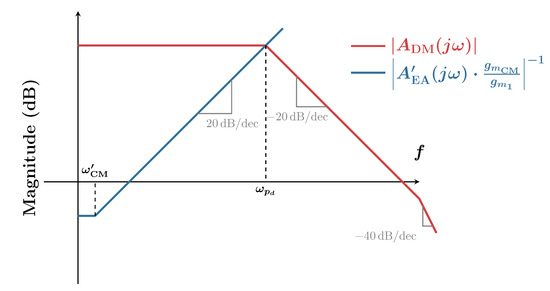
Figure 5.
ROC curves for the compensated single-loop design.
From Figure 5, the following relationship holds
which means that the bandwidth of the CMFB loop has to be considerably lower than that of the differential loop as expected. Indeed, considering a differential loop DC gain of 80 dB, we can see that the bandwidth of the common-mode loop may have to be up to 4 orders of magnitudes lower than that of the differential loop. This implies that the CMFB loop may fail to reject CM disturbances that lie within the bandwidth of interest (differential loop bandwidth).
2.1.2. Multiple Loops
In the case of multiple loops, Figure 6 shows the CM equivalent circuit.
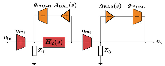
Figure 6.
Small-signal model of the CM equivalent circuit for the multi-loop design.
First, we note that the loops do not interact with each other, and therefore their stability margins can be studied independently. It is straightforward to show that the loop gains are given by
with the error amplifier gains modeled by
Starting with the simpler self-loop at the output (), note that the poles are given by and where represents the output conductance of the third stage, represents the load capacitance and represents the total loading effect of any part of the Miller compensation network (used to compensate the differential-mode loop of the core three-stage amplifier) that is connected to the output. If, by proper design, is set at a high enough frequency, the self-loop is compensated by the load capacitance and does not need additional compensation.
Turning our attention to , we first start by noting that
where and are frequency-dependent factors needed to replace the poles and zeros of with those of . We can therefore express as follows:
This means that, if the roots of and are positioned judiciously and is large, an ROC that results in sufficient PM can be obtained without compensation.
As a concrete example, assume that the differential-mode amplifier is compensated using single-Miller-capacitor compensation (SMC) [12] with a nulling resistor to cancel the effect of the RHP zero as shown in Figure 7 (this figure is the half-circuit equivalent of the differential-mode loop). In the figure,
where and represent the output conductance and output capacitance of stage i respectively, with being the load capacitance .
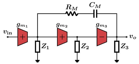
Figure 7.
Example of the compensation strategy of the differential-mode loop.
The transfer function of the inner amplifier is therefore given by
and
so that
where
This allows us to sketch the ROC curves as shown in Figure 8 with denoting the dominant pole of the differential-mode gain and denoting the factor so that . It can be seen that the ROC is 20 dB/decade, leading to a good PM.
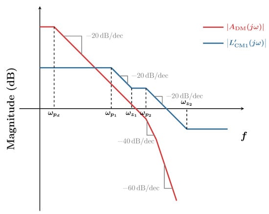
Figure 8.
ROC curves for the first single-Miller-capacitor compensation (CMFB) loop with the SMC compensation example.
In conclusion, the single-loop solution requires buffered Miller capacitor compensation for the CMFB loop to ensure its stability without affecting the dynamics of the differential-mode loop. On the other hand, the multi-loop solution can achieve stability for both loops without requiring additional compensation capacitors. This result aligns well with intuition because both loops in the multi-loop topology have lower order than the loop in the single-loop topology and may therefore be stabilized simply by proper design, without requiring bulky compensation capacitors.
2.2. Linearity
This section investigates the impact the CMFB loop generated harmonics can have in the overall spectral purity of the differential signals. The following assumptions are made to define the scope of the study:
- The common-mode error amplifier non-linearity converts the second harmonic of the differential-mode voltage it senses into a common-mode so that its response is given bywhere is the common-mode component of the voltage sensed by the common-mode error amplifier and is the differential component of the same voltage.
- The common-mode amplifier will only respond to the components given in (17). In other words, other harmonic components generated by intermediate stages are negligible in the way they affect the common mode error amplifier.
In addition, the following conventions will be followed:
- We will assume that the input voltage produces differential- and common-mode signals at the output of the first stage given by and , respectively.
- The non-linearity of the intermediate transconductance stages is modeled by:where v is the transcondutor’s input voltage and i its output current. and represent, respectively, the second- and third-order transconductance gain coefficients. Higher-order non-linear terms are neglected.
The main mechanism by which the CMFB sensor non-linearity affects the linearity of the differential output signal can be described as follows [13]:
- The non-linearity of the CM error amplifier creates the second harmonic of the differential voltage it senses which appears as a common-mode disturbance.
- The non-linearity of the intermediate stages can mix this second harmonic with the fundamental and create a third-order (and hence differential-mode) distortion.
Note that the non-linearity contribution of the CMFB loop can be reduced to nearly zero if a resistive common-mode sensor is used. In this case, both CMFB loop implementations will yield similar linearity performance. However, this approach often requires the use of large resistors to avoid loading the main gain stages. The large resistors introduce noise, consume a substantial area and render the CMFB loop more difficult to stabilize because they introduce a low-frequency pole at the input of the error amplifier, making this approach impractical for many applications.
2.2.1. Single Loop
For this section, we solve the model of Figure 2 for the the differential output voltage in terms of the other quantities under the assumptions and conventions stated above. The buffered Miller capacitor compensation path is neglected in order to keep the analysis simple, since it is not expected to significantly impact linearity.
The output differential voltage can be expressed as
where
and denotes third-order harmonic distortion. We can see that the first two terms in (20) are due to the non-linearity of the CMFB error amplifier converted into a differential-mode distortion by the non-linearity in the intermediate stages.
2.2.2. Multiple Loops
Using the same assumptions as before, we get the following expression for of the multi-loop solution:
Now, we consider only the non-linear terms of (20) and (21) contributed by the CM error amplifier non-linearity () and denote the resulting distortion factors by . We get
This ratio is much less than unity, which means that an amplifier using a single CMFB loop will have more distortion than the one that uses multiple loops. Intuitively, this is because in the single-loop case, the distortion products from the second stage are amplified by the third stage inside the loop.
2.3. Noise
For noise analysis, we are interested in the contribution of the CMFB loops to differential-mode noise. As a result, we do not consider the noise from the CM error amplifier as it will appear as CM noise in the differential-mode loop and be rejected by the following stages assuming good matching. It should also be noted that, when deriving the expression for the input-referred differential-mode noise, noise shaping by the CM loop must not be considered since it will only affect common-mode noise.
2.3.1. Single Loop
The only noise sources we need to consider in this case are and the buffers used in the compensation of the CMFB loop. Note that there will be two such buffers with uncorrelated noise contributions, which will not therefore appear as CM noise. The noise current from is simply referred to the input by dividing it by . The input-referred noise of the buffer () is referred to the input by dividing it by the first and second stage gains and we have the single-ended input-referred noise voltage given by
where is the excess channel noise factor. Since the gain of the first two stages is large, we can write
The differential noise voltage is simply twice the single-ended noise voltage [14]:
2.3.2. Multiple Loops
By similar reasoning to the single-loop case, we will consider the transconductors as the only noise sources. The noise from is handled similarly to the single-loop case. Meanwhile, the single-ended output noise voltage contribution of is given by
so that the input-referred noise due to it alone is given by
The input-referred differential noise voltage in this case will be given by
and again, we may neglect the second component to find
The above analysis shows that, for equal power budgets, the two solutions exhibit nearly identical noise performance. Indeed, as will be shown in the transistor-level implementation, and have the same bias current going through them (current re-use) meaning that with the same device sizes and bias currents, the approximate input-referred noise voltage expressions for the two solutions are identical.
2.4. Common-Mode Disturbance Rejection
A very important metric for the performance of CMFB loops is their ability to reject (attenuate) CM disturbances. This section will examine the CM rejection performance of each solution in response to 2 types of CM disturbance:
- A CM current injected at the output nodes.
- A CM voltage imposed on the input nodes.
2.4.1. Single Loop
In the single-loop case, Figure 9 shows the two types of disturbances added to the model with denoting and is the gain of the error amplifier after CMFB loop compensation.
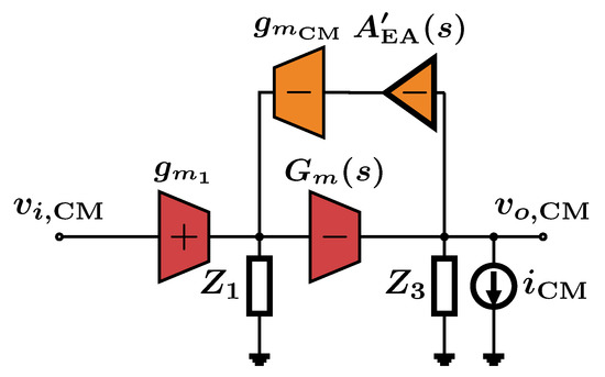
Figure 9.
CM equivalent small-signal model for CM disturbance rejection in the single-loop solution.
In this case, we can prove that
The above expressions show that CM disturbances at the output get rejected with the full loop gain but since this loop gain is compensated, it will have a very low bandwidth. So output common-mode disturbance rejection is possible only over a very narrow bandwidth compared to the bandwidth of the differential-mode loop. On the other hand, a CM input voltage disturbance will be rejected with only modest gain and very low bandwidth.
2.4.2. Multiple Loops
In this case, the disturbance model is shown in Figure 10 where and denote, respectively and .
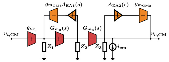
Figure 10.
CM equivalent small-signal model for CM disturbance rejection in the multi-loop solution.
In this case, we have
We immediately see that the output disturbance gets rejected with a lower gain than in the single-loop case but over a much wider bandwidth. In the case of an input voltage disturbance, the disturbance gets rejected with a higher-gain than the single-loop case over a comparable bandwidth. This assumes that the bandwidth of the second CM loop is high enough that the rejection bandwidth will be fixed by loop 1. We therefore conclude that the single-loop case is better at rejecting output CM disturbances at low-frequency while the multi-loop case is better at rejecting input CM disturbances.
3. Design Case Study
In this section, transistor-level simulation results (using Spectre ®) for a 3-stage OTA design will be used to corroborate the theoretical discussions of the previous section. First, some performance specifications are established, then a specific topology is selected and designed for both CMFB implementations. One of the main goals of the approach taken here is to design both solutions with equal gain and similar power consumption. It is important for both designs to have these similar metrics so that a fair comparison can be made between the two solutions.
All the design and simulation results reported here reference a TSMC nm CMOS process with a power supply of 1.8 V.
3.1. Performance Specifications
The design of the OTA will target a unity-gain frequency (UGF) of MHz, where the desired application in this case is an active-RC filter with a MHz corner frequency, commonly used in multiple receiver standards [15]. The capacitive load is assumed to be pF.
As stated in [16,17,18,19], the design of 3-stage OTAs is best approached in the time domain. With the target application in mind, we note that a MHz signal has a period of ns. As a good rule of thumb, therefore, we will specify that the OTA’s settling time should not exceed ns (i.e., 10% of the signal’s period).
3.2. Topology Choice and System-Level Design
Since the chosen capacitive load is not large, choosing a topology with a compensated inner amplifier will result in a more power-efficient design. In this case, the nested -C topology [20] is chosen. Figure 11 shows the half-circuit equivalent small-signal model of this topology.
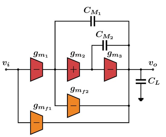
Figure 11.
Half-circuit equivalent small-signal model for the nested topology.
We denote the output conductance and parasitic capacitance of stage i by and , respectively. Assuming and , the transfer function of the nested OTA is given by [20]:
so that the non-dominant pole pair is defined by its natural frequency and quality factor Q given by
Defining , we can generate a contour plot for the normalized settling time in the space via numerical simulations. The result is shown in Figure 12. Note that the settling time definition used here is the time it takes for the amplifier’s output to reach, and stay, within 1% of its final steady-state value.
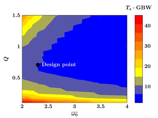
Figure 12.
Contour plots of the normalized settling time ( Gain-Bandwidth Product (GBW) to the right) as a function of non-dominant pole parameters ( and Q), final design point highlighted.
Assuming proper pole-zero cancellation and pole placement, the amplifier’s response can be approximated as a one-pole system with . Since the intended UGF is MHz, we need a normalized settling time of
Using Figure 12 as reference, we thus choose and as highlighted in the figure. From the expression for Q we have
Using this value and the equation for , we get mS. Assuming pF and pF, we get μS and μS, thus completing the design process.
To verify the accuracy of this system design, a macromodel was built with ideal voltage-controlled current sources and simulation results required to be adjusted to obtain the required UGF and settling time. The final value chosen was μS. Other parameters of the design remained as chosen above. Figure 13 shows the Bode plot of the gain of the simulated macromodel while Figure 14 shows its unit step response under unity-gain feedback. It can be seen that the target specifications were met by this choice of system parameter values.
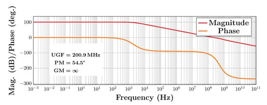
Figure 13.
Transfer function of the macromodel of the designed Operational Transconductance Amplifier (OTA).
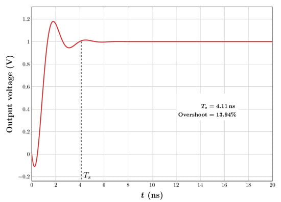
Figure 14.
Step response of the macromodel of the designed OTA.
3.3. Transistor-Level Amplifier
Figure 15 shows the transistor implementation of the fully-differential nested -C OTA with the transistors belonging to different sub-blocks highlighted. It should be noted that is set by the CMFB loop in both solutions while is set by static bias in the single-loop solution and by the second CMFB loop in the multi-loop solution. Both and are highlighted in red in the figure.
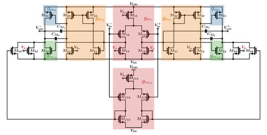
Figure 15.
Schematic of the fully differential nested OTA.
As can be seen in Figure 15, devices implement while devices implement exploiting current re-use to limit power consumption and, as noted above, leading the ratio to be the same in both solutions. Devices and form a current mirror that converts the polarity of to positive as required to make the feedback through the Miller capacitor negative. Devices supply extra current to the two output branches to ensure that has the required value.
The design of the amplifier core was approached as follows:
- Devices were sized to provide the required with a of mV.
- Devices were sized to sink the current of with a of mV.
- The stage was sized in an identical fashion to the stage to ensure .
- Devices were sized to have the same current density as with the ratio of their sizing being devices were matched to .
- Devices and were sized equally to provide current mirroring with a of mV.
- Devices were sized to have the same current density as and with the ratio of their sizing being .
- Devices were initially matched to to ensure but ended up being made larger to create a left-half-plane (LHP) zero and improve the phase margin in the presence of an additional parasitic pole (due to resistive feedback when the core amplifier is connected as a unity-gain inverting amplifier).
- Devices were matched to devices .
- Devices were matched to in current density. They were sized to provide a current equal to the current required by minus the currents supplied by and .
Table 1 shows the final device sizes in the core amplifier in accordance with the above design procedure. Table 2 shows the capacitor values used with denoting the capacitor used to compensate the CMFB loop in the single-loop solution.

Table 1.
Device sizes for the schematic in Figure 15.

Table 2.
Capacitor values for the schematic in Figure 15. denotes the capacitor used to compensate the Common-Mode Feedback (CMFB) loop in the single-loop solution.
3.4. Design of Auxiliary Amplifiers
There are three different types of auxiliary amplifiers used in the design:
- A low-gain CM error amplifier.
- A high-gain CM error amplifier (used to provide a high enough gain in the second loop of the multi-loop solution to ensure good CM output voltage accuracy)
- An amplifier configured in unity-gain feedback to act as a buffer for the compensation of the CMFB loop in the single-loop solution.
Figure 16 shows the error amplifiers used in the single-loop solution and the first loop of the multi-loop solution while Figure 17 shows the high-gain amplifier used in the second loop of the multi-loop solution as well as the unity-gain buffer used to compensate the CMFB loop of the single-loop solution. The basic underlying structure of all 4 amplifiers is the same but their wiring is different. It should be noted that CM error amplifiers deliberately use the differential-difference-amplifier-based CM voltage sensing (instead of using resistors to sense the CM voltage) because this makes the CM sensor more non-linear [21] and therefore emphasizes the effect of its non-linearity on the linearity of the amplifier.
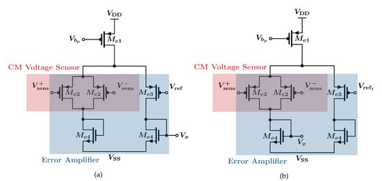
Figure 16.
Low-gain auxiliary amplifiers: (a) Error amplifier for the CMFB loop of the single-loop solution (b) Error amplifier for the CMFB loop 1 of the multi-loop solution.
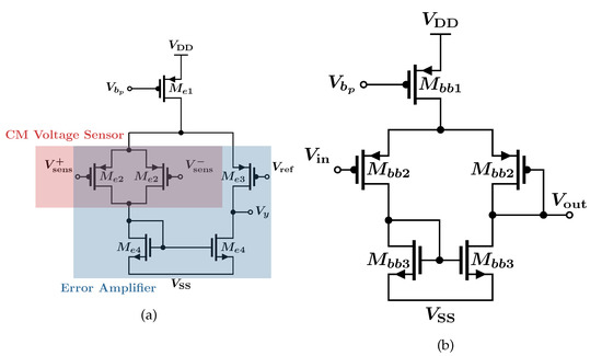
Figure 17.
High-gain auxiliary amplifiers: (a) Error amplifier for CMFB loop 2 of the multi-loop solution (b) Amplifier in unity-gain feedback acting as a buffer for the compensation of the CMFB loop in the single-loop solution.
The approach used to design these amplifiers was as follows:
- Start by assigning a portion of the current budget to the error amplifier with respect to the devices. For the case of the single-loop solution, the current through devices – was the same as the current in , for loop 1 of the multi-loop solution, the same devices were made to carry only half of the current of while in loop 2 they were made to carry of the current of so that the power consumption of the two solutions remains the same.
- Size the input devices – with the appropriate . A value of mV was sufficient for the single-loop case and loop 2 of the multi-loop case because the reference voltage is set at mid-supply. In the case of loop 1 of the multi-loop case, it was necessary to reduce the to mV because the reference voltage driving these devices () is higher than mid-supply (∼1.1 V). Each of the devices is half the size of the corresponding device.
- Finally, devices are matched in current density to the device they will be connected to and sized in accordance with the ratio of currents chosen in the first step.
- The buffer devices are sized identically to the single-loop error amplifier devices but connected differently as shown in Figure 17.
Table 3 shows the final sizes of the devices used in the auxiliary amplifiers in the single-loop solution while Table 4 shows those of the multi-loop solution.

3.5. Auxiliary Amplifier Responses
To make sure the auxiliary amplifiers work as expected, their transfer functions were simulated separately and are shown in Figure 18. In all cases, the single-pole approximation seems warranted except in the single-loop case where the amplifier has a RHP zero due to the drain-to-gate device capacitance of devices in Figure 16a. This does not affect the stability of the CMFB loop significantly and using a compensation capacitor to stabilize the CMFB loop is still possible.
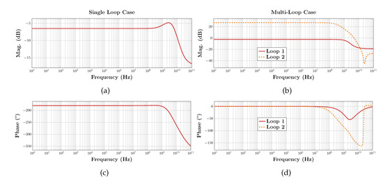
Figure 18.
Transfer function of the CMFB error amplifiers used in the different CMFB loops, (a) magnitude and (c) phase for the single-loop case and (b) magnitude and (d) phase for the multi-loop case.
3.6. Reference Voltage Generation
To generate the internal reference shown in Figure 16b, recall that the devices were matched in current density to the devices, so a good voltage level to set the gates of is the (common-mode) voltage at the gates of . In order to generate this CM voltage, a replica reference generator circuit (shown in Figure 19) was used. In the figure, the devices have the same size as the devices with the gate of each device connected to one of the two devices. The device, therefore, has twice the size of the two devices in the core amplifier.
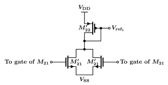
Figure 19.
Replica reference generator for the CM error amplifier of Figure 16b.
3.7. DC Simulation Results
Table 5 shows the DC simulation results for both solutions along with the specified values in the initial design. It is seen that both solutions have very similar power budgets and have achieved the specified values of all the transconductances (with the exception of ) as discussed above.

Table 5.
DC simulation results for the two solutions along with the target values specified in the initial design.
3.8. Differential Loop Response
For this test, the differential loop gain was simulated using two different methods—with the amplifier in open loop (using ac analysis) and with the OTA configured as a unity-gain inverting amplifier with kΩ feedback resistors (using stability analysis). In addition, the settling time performance is tested by injecting a differential step superimposed on top of the input common mode voltage to the OTA set in unity-gain inverting amplifier configuration.
Figure 20 shows the transfer function of the differential-mode loop of the single-loop solution. Along with measuring the loop gain in two ways as explained above, the macromodel used for system design was fed with the parameter values obtained from the DC simulation and the loop’s transfer function was plotted. It can be seen that the macromodel is fairly accurate and sufficient for initial design. The discrepancy between the macromodel results and the simulation results at high frequencies is due to parasitic capacitance and other second-order effects not accounted for in the macromodel. In addition, the closed-loop simulation takes into account the parasitic pole due to the interaction of the feedback resistors with the amplifier’s input capacitance, which accounts for the discrepancy between the two simulation methods.
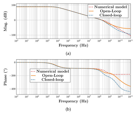
Figure 20.
Transfer function of the differential loop in the single-loop solution (a) magnitude and (b) phase.
Figure 21 shows the single-ended and differential output voltage in response to the input step pulse for the single-loop solution. This confirms the stability of the loop assessed from the frequency-domain results.
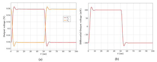
Figure 21.
Differential-mode step response of the single-loop solution: (a) single-ended output voltages and (b) differential output voltage.
Figure 22 and Figure 23 show the corresponding results for the multi-loop solution with similar conclusions. Note that the single-ended output response exhibits some CM ringing because the CMFB loop has lower phase margin than its single-loop counterpart as will be discussed in the next section.
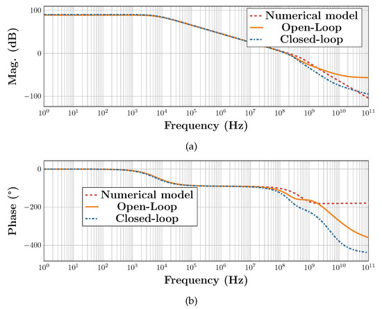
Figure 22.
Transfer function of the differential loop in the multi-loop solution (a) magnitude and (b) phase.
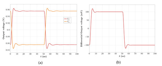
Figure 23.
Differential-mode step response of the multi-loop solution: (a) single-ended output voltages and (b) differential output voltage.
Table 6 summarizes the simulation results for both cases. It can be seen that the settling time specification was not met due to the parasitic pole not being accounted for in the macromodel.

Table 6.
Differential-mode results for both solutions.
3.9. CMFB Loop Responses
The frequency- and time-domain responses for the CMFB loops were tested for both solutions in an inverting amplifier configuration. The time-domain response was tested by injecting μA CM current step at the output nodes of the amplifier and measuring the CM output voltage.
Figure 24 shows the frequency-domain results for the single-loop case while Figure 25 shows the results for the multi-loop case.
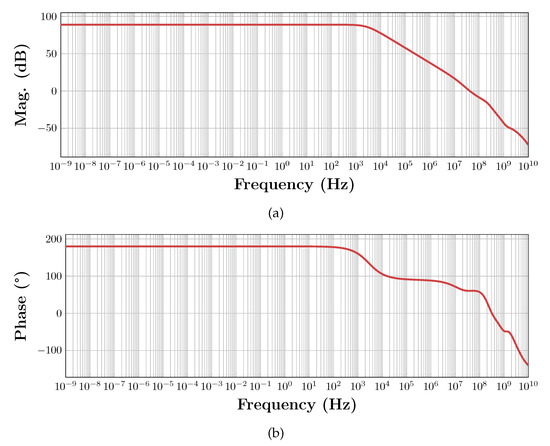
Figure 24.
Transfer function of the CMFB loop in the single-loop case (a) magnitude and (b) phase.
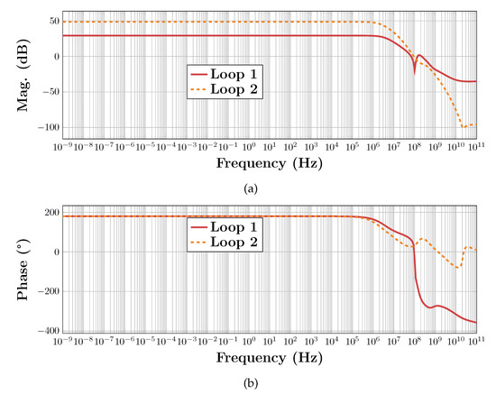
Figure 25.
Transfer functions of the CMFB loops in the multi-loop case: (a) magnitude and (b) phase.
The transient responses (in both cases) for the loop settling after a CM current disturbance injected at the output are shown in Figure 26. It should be noted that, due to the poorer PM of loop 2, the multi-loop case takes a slightly longer time to settle. In addition, because of its lower DC gain, there is a mV static error in the CM output voltage when the CM disturbance is injected compared to normal conditions.
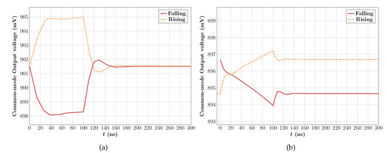
Figure 26.
CM step response (a) Single-loop and (b) Multi-loop.
Table 7 summarizes the results for all CMFB loops. It can be seen that the CMFB loop in the single-loop case is more stable than loop 2 in the multi-loop case. If more stability is needed in the multi-loop case, compensation capacitors can be added at the expense of area and power (since the capacitors will have to be buffered as well). The results, however, demonstrate that it is possible to design the multi-loop implementation for stability without requiring the use of compensation capacitors, thereby saving on area (and power, by avoiding the use of power-hungry voltage buffers).

Table 7.
Common-mode results for both solutions.
3.10. Linearity
To assess the linearity of the amplifiers, a differential sinusoidal signal with kHz frequency was applied at the input (superimposed on the input CM level) with the amplifier set in unity-gain feedback. The amplitude of the input signal was swept and the of the output differential voltage was obtained. The results are shown in Figure 27. The results clearly confirm the theoretical analysis where the linearity of the multi-loop solution is seen to be superior to the single-loop one. Given the fact that both amplifiers have identical differential-mode loops (particularly, identical overdrive voltages for the input stages), it stands to reason that the origin of the difference in performance lies in the CMFB implementation.
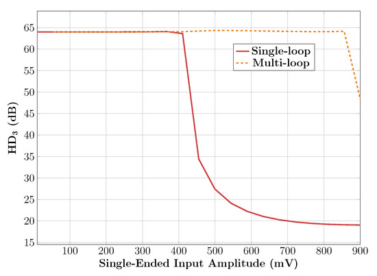
Figure 27.
Comparison of the linearity of the CMFB solutions.
3.11. Noise
To analyze noise performance, each OTA was put in inverting unity-gain feedback configuration, the noise analysis was used to obtain the spectrum of the input-referred noise. Figure 28 shows the noise spectra for both cases. The simulation results are in agreement with analysis since the two spectra are virtually identical as illustrated by the bottom curve of Figure 28 showing the difference between the single-loop spectrum and the multi-loop spectrum.
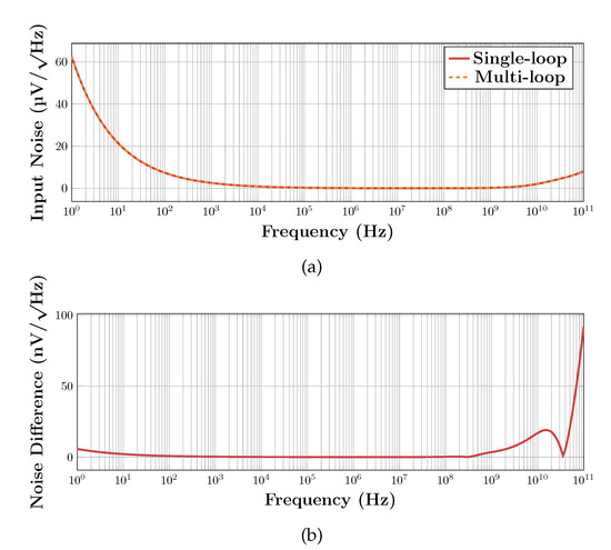
Figure 28.
Input-referred noise for both cases: (a) input-referred noise and (b) difference between the input-referred noise in the single-loop case and that in the multi-loop case.
3.12. CM Disturbance Rejection
To simulate the CM disturbance rejection, an AC input CM voltage disturbance is injected to the amplifiers in a unity-gain inverting configuration, measuring the spectrum of the output CM voltage. The result is shown in Figure 29 and confirms the theoretical results.
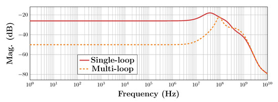
Figure 29.
Input common-mode disturbance rejection.
3.13. Filter Implementation
To demonstrate the impact of the CMFB loop implementation in a practical setting, each of the OTAs was used to implement an active-RC biquad implementing the second-order Butterworth low-pass function with a cut-off frequency of 20 MHz. Figure 30 shows the final design of the biquad filter. The OTAs used in the biquad are both using the same CMFB topology (i.e., 2 single-loop CMFB OTAs or 2 multi-loop CMFB OTAs).
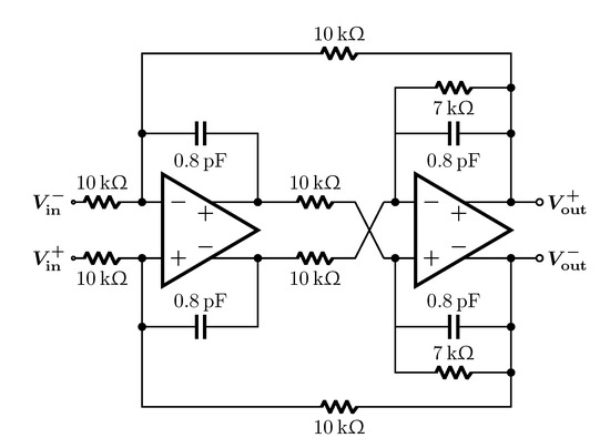
Figure 30.
Active-RC biquad implementing the Butterworth low-pass function with 20 MHz cut-off frequency.
The biquad filter was simulated twice—once with the single-CMFB-loop OTA and once with the multi-CMFB-loop OTA used for its implementation. Figure 31 shows the transfer function of the transistor-level biquad circuit in both cases (both OTA implementation cases exhibit the same biquad transfer function) compared to the ideal transfer function. It is noted that the transistor-level implementations succeed in implementing the required transfer function at low-to-moderate frequencies and the discrepancies present in high frequencies are due to parasitics and second order effects.
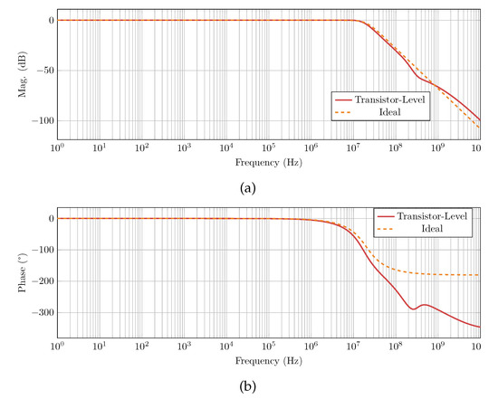
Figure 31.
Biquad response. Transistor-level data is the same for both OTA implementations: (a) magnitude and (b) phase.
As can be seen in Figure 27, the linearity improvement due to the use of multiple CMFB loops only becomes apparent at large input amplitudes (i.e., in the strong non-linearity regime). As such, the -dB compression point is used as a metric to emphasize the difference in the filter’s linearity performance in the region of strong non-linearity. Compression can be a significantly damaging effect on receiver chains (a common application of filters), either as a result of the type of modulation employed or due to the presence of large in-bandwidth blockers appearing from interference or transmitter leakage [22]. Figure 32 shows the compression point curves for both implementations.
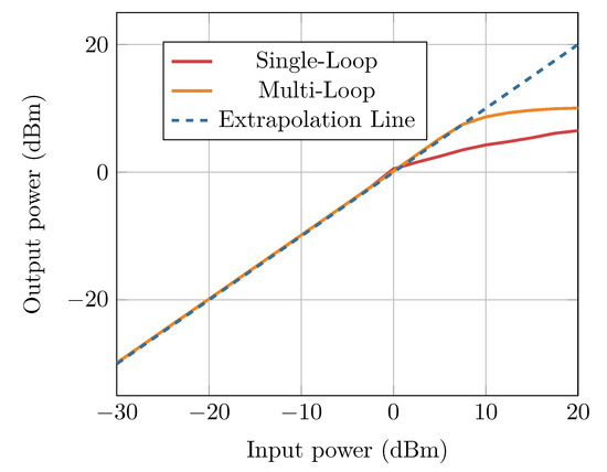
Figure 32.
1-dB compression point curves for both biquad implementations.
The curves were obtained by stimulating the input with the two-tone test frequencies of 4.5 MHz and 4.6 MHz [15]. The input amplitude was swept and the output amplitude at the fundamental tone was observed (4.5 MHz). This method was used because the multi-loop biquad implementation did not exhibit compression when the input was a single tone. Likely due to the drop in gain inside the loop at the higher frequency harmonics. From the curves, it can be seen that the input-referred -dB compression point () for the single-loop biquad is 2.34 dBm while that for the multi-loop biquad is 9.08 dBm. This demonstrates that the relative linearity merits of the multi-loop implementation still hold when the OTA is used in a relevant high-linearity application. Table 8 shows a comparison of the filter design with the state of the art. Although the results from this work are simulation-only, the values of give additional context to understand the significant performance advantage to be gained by choosing the proper CMFB implementation, while remaining competitive in regards to power per pole.

Table 8.
Comparison of filter metrics with state of the art.
4. Discussion
Table 9 summarizes the relative merits of the two CMFB implementations. Even though the initial intuition of a designer may be to use a single CMFB loop when implementing a fully differential 3-stage OTA, it turns out the single-loop solution is not necessarily less expensive or complex than the multi-loop one, because it necessitates the use of compensation capacitors and buffers for the CMFB loop to guarantee stability. While there is no significant difference between the two approaches regarding noise performance, the multi-loop implementation has a clear advantage in terms of input CM disturbance rejection and linearity. Thus, the multi-loop solution should be the preferred implementation for CMFB when the amplifier is intended for a high-linearity or high-frequency application. However, the higher rejection gain to output CM disturbances (albeit at a reduced bandwidth) may be a more critical specification in some applications, particularly if the design is not intended for high-frequency operation, which relaxes the stability constraints in the single-loop implementation. Furthermore, there may be other parameters to consider when deciding the type of CMFB implementation, such as power supply rejection, which depends heavily on the specific transistor implementation, and therefore is beyond the scope of this work’s topology agnostic analysis.

Table 9.
Qualitative comparison of the performance of the two CMFB implementations.
5. Conclusions
This paper explores two possible CMFB implementations for fully differential three-stage OTAs—using a single loop or two independent loops. The merits of each approach are evaluated in terms of their impact on stability, linearity, noise and CMR. We demonstrate the advantages of the multi-loop solution when targeting high-linearity or high-frequency applications and the single-loop superior output CM rejection.
The preceding conclusions are supported through a topology agnostic theoretical analysis and are verified through simulation of a design case example (Nested -C OTA in TSCM 180 nm process). A 2nd order Butterworth Low-Pass Filter was also simulated using both approaches to provide an application example and to demonstrate how the design choice of the CMFB implementation can impact system-level performance, showing that using a multi-loop CMFB can improve the 1-dB compression point of the filter by more than 6 dBs compared to a single loop implementation, without any changes in the differential path.
Author Contributions
Conceptualization, J.R.; formal analysis, J.R. and S.S.-A; investigation, J.R. and J.J.E.-L.; writing—original draft preparation, J.R.; writing—review and editing, S.S.-A., J.J.E.-L. and O.M.-T.; supervision, O.M.-T. and E.S.-S.; funding acquisition, E.S.-S. All authors have read and agreed to the published version of trhe manuscript.
Funding
This work was funded in part by Texas Instruments and in part by the National Science Foundation under Grant No. ECCS-2000851.
Conflicts of Interest
The authors declare no conflict of interest.
Abbreviations
The following abbreviations are used in this manuscript:
| CM | Common-Mode |
| CMR | Common-Mode Rejection |
| CMFB | Common-Mode Feedback |
| GBW | Gain-Bandwidth Product |
| GM | Gain Margin |
| LHP | Left-Half Plane |
| OTA | Operational Transconductance Amplifier |
| PM | Phase Margin |
| RHP | Right-Half Plane |
| ROC | Rate of Closure |
| SMC | Single-Miller Capacitor |
| UGF | Unity-Gain Frequency |
References
- Carusone, T.C.; Johns, D.A.; Martin, K. Analog Integrated Circuit Design; John Wiley & Sons: Hoboken, NJ, USA, 2011. [Google Scholar]
- Palumbo, G.; Pennisi, S. Design Methodology and Advances in Nested-Miller Compensation. IEEE Trans. Circuits Syst. Fundam. Theory Appl. 2002, 49, 893–903. [Google Scholar] [CrossRef]
- Cheng, Q.; Li, W.; Tang, X.; Guo, J. Design and Analysis of Three-Stage Amplifier for Driving pF-To-nF Capacitive Load Based on Local Q-Factor Control and Cascode Miller Compensation Techniques. Electronics 2019, 8, 572. [Google Scholar] [CrossRef]
- Xu, G.; Embabi, S.H.K. A systematic approach in constructing fully differential amplifiers. IEEE Trans. Circuits Syst. II Analog. Digit. Signal Process. 2000, 47, 1547–1550. [Google Scholar] [CrossRef]
- Saxena, V.; Baker, R.J. Indirect Compensation Techniques for Three-Stage Fully-Differential Op-Amps. In Proceedings of the 2010 53rd IEEE International Midwest Symposium on Circuits and Systems; IEEE: New York, NY, USA, 2010; pp. 588–591. [Google Scholar] [CrossRef]
- Saxena, V.; Balagopal, S.; Baker, R.J. Systematic Design of Three-Stage Op-Amps using Split-Length Compensation. In Proceedings of the 2011 IEEE 54th International Midwest Symposium on Circuits and Systems (MWSCAS), Seoul, Korea, 7–10 August 2011; IEEE: New York, NY, USA, 2011; pp. 1–4. [Google Scholar] [CrossRef]
- Golabi, S.; Yavari, M. Design of CMOS three-stage amplifiers for fast-settling switched-capacitor circuits. Analog. Integr. Circuits Signal Process. 2014, 80, 195–208. [Google Scholar] [CrossRef]
- Pernici, S.; Nicollini, G.; Castello, R. A CMOS low-distortion fully differential power amplifier with double nested Miller compensation. IEEE J. Solid-State Circuits 1993, 28, 758–763. [Google Scholar] [CrossRef]
- Wait, J.; Huelsman, L.; Korn, G. Introduction to Operational Amplifier Theory and Applications; McGraw-Hill: New York, NY, USA, 1975. [Google Scholar]
- Yan, Z.; Mak, P.I.; Law, M.; Martins, R. A 0.016-mm2 144-W Three-Stage Amplifier Capable of Driving 1-To-15 nF Capacitive Load With > 0.95-MHz GBW. IEEE J. Solid-State Circuits 2013, 48, 527–540. [Google Scholar] [CrossRef]
- Grasso, A.D.; Marano, D.; Palumbo, G.; Pennisi, S. High-Performance Three-Stage Single-Miller CMOS OTA With No Upper Limit of CL. IEEE Trans. Circuits Syst. II Express Briefs 2018, 65, 1529–1533. [Google Scholar] [CrossRef]
- Fan, X.; Mishra, C.; Sanchez-Sinencio, E. Single Miller Capacitor Frequency Compensation Technique for Low-Power Multistage Amplifiers. IEEE J. Solid-State Circuits 2005, 40, 584–592. [Google Scholar]
- Mohieldin, A.N. High Performance Continuous-Time Filters for Information Transfer Systems. Ph.D. Thesis, Texas A&M University, College Station, TX, USA, 2003. [Google Scholar]
- Behzad, R. Design of Analog CMOS Integrated Circuits, 3rd ed.; McGraw-Hill: New York, NY, USA, 2001. [Google Scholar]
- Amir-Aslanzadeh, H.; Pankratz, E.; Sanchez-Sinencio, E. A 1-V +31 dBm IIP3, Reconfigurable, Continuously Tunable, Power-Adjustable Active-RC LPF. IEEE J. Solid-State Circuits 2009, 44, 495–508. [Google Scholar] [CrossRef]
- Pugliese, A.; Amoroso, F.; Cappuccino, G.; Cocorullo, G. Settling Time Optimization for Three-Stage CMOS Amplifier Topologies. IEEE Trans. Circuits Syst. I Regul. Pap. 2009, 56, 2569–2582. [Google Scholar] [CrossRef]
- Seth, S.; Murmann, B. Settling Time and Noise Optimization of a Three-Stage Operational Transconductance Amplifier. IEEE Trans. Circuits Syst. I Regul. Pap. 2013, 60, 1168–1174. [Google Scholar] [CrossRef]
- Riad, J.; Estrada-López, J.J.; Sánchez-Sinencio, E. Classification and Design Space Exploration of Low-Power Three-Stage Operational Transconductance Amplifier Architectures for Wide Load Ranges. Electronics 2019, 8, 1268. [Google Scholar] [CrossRef]
- Giustolisi, G.; Palumbo, G. Efficient Design Strategy for Optimizing the Settling Time in Three-Stage Amplifiers Including Small- and Large-Signal Behavior. Electronics 2021, 10, 612. [Google Scholar] [CrossRef]
- You, F.; Embabi, S.H.K.; Sanchez-Sinencio, E. Multistage Amplifier Topologies With Nested Gm-C Compensation. IEEE J. Solid-State Circuits 1997, 32, 2000–2011. [Google Scholar] [CrossRef]
- Duque-Carrillo, J.F. Control of the Common-Mode Component in CMOS Continuous-Time Fully Differential Signal Processing. Analog. Integr. Circuits Signal Process. 1993, 4, 131–140. [Google Scholar] [CrossRef]
- Razavi, B. RF Microelectronics, 2nd ed.; Pearson Education: London, UK, 2011. [Google Scholar]
- Lim, J.; Kim, J. A 20-kHz 16-MHz Programmable-Bandwidth 4th Order Active Filter Using Gain-Boosted Opamp With Negative Resistance in 65-nm CMOS. IEEE Trans. Circuits Syst. II Express Briefs 2019, 66, 182–186. [Google Scholar] [CrossRef]
- Xu, Y.; Venkatachala, P.K.; Leuenberger, S.; Moon, U.K. A 7.5mW 35–70MHz 4th-order semi-passive charge-sharing band-pass filter with programmable bandwidth and 72 dB stop-band rejection in 65 nm CMOS. In Proceedings of the 2016 IEEE Radio Frequency Integrated Circuits Symposium (RFIC), San Francisco, CA, USA, 22–24 May 2016; IEEE: New York, NY, USA, 2016; pp. 162–165. [Google Scholar] [CrossRef]
- Lavalle-Aviles, F.; Sánchez-Sinencio, E. A 0.6-V Power-Efficient Active-RC Analog Low-Pass Filter With Cutoff Frequency Selection. IEEE Trans. Very Large Scale Integr. (Vlsi) Syst. 2020, 28, 1757–1769. [Google Scholar] [CrossRef]
- Park, C.; Tavares, Y.A.; Lee, J.; Wo, J.; Lee, M. 5th-Order Continuous-Time Low-Pass Filter Achieving 56 MHz Bandwidth 30.5 dBm IIP3 with a Novel Low-Distortion Amplifier. IEEE Trans. Circuits Syst. II Express Briefs 2020. [Google Scholar] [CrossRef]
Publisher’s Note: MDPI stays neutral with regard to jurisdictional claims in published maps and institutional affiliations. |
© 2021 by the authors. Licensee MDPI, Basel, Switzerland. This article is an open access article distributed under the terms and conditions of the Creative Commons Attribution (CC BY) license (https://creativecommons.org/licenses/by/4.0/).