
A 17.8–34.8 GHz (64.6%) Locking Range Current-Reuse Injection-Locked Frequency Multiplier with Dual Injection Technique


Abstract
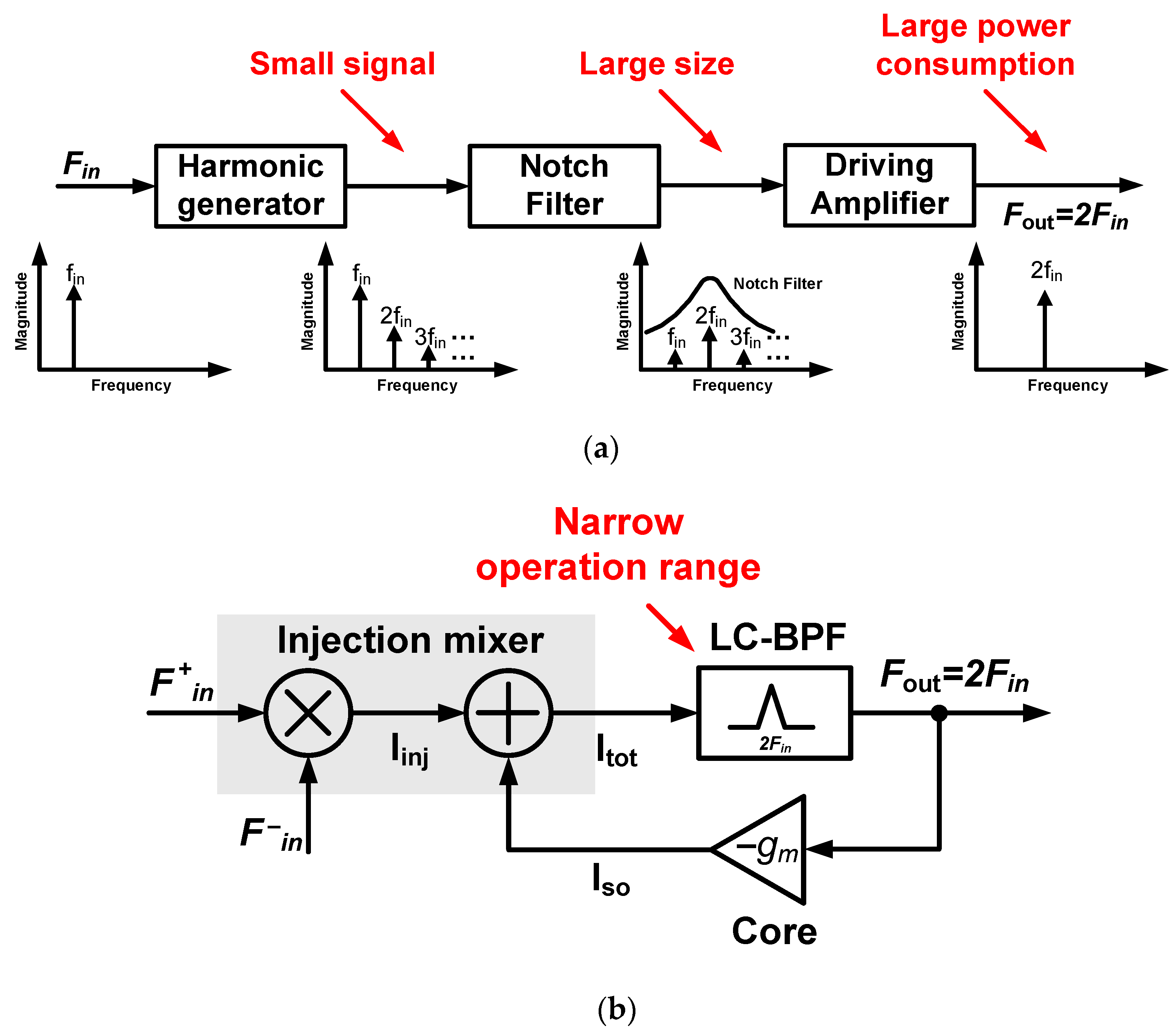
:1. Introduction
2. Proposed CR-ILFM
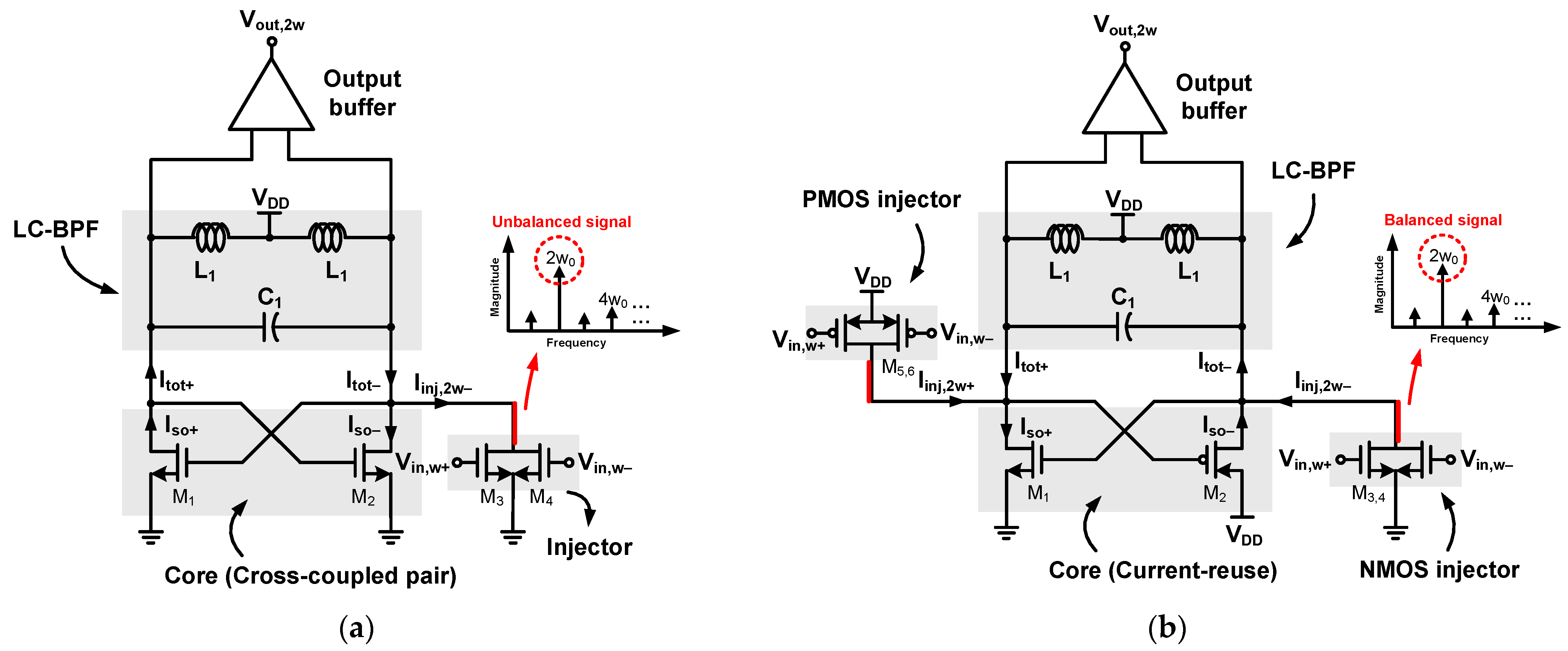
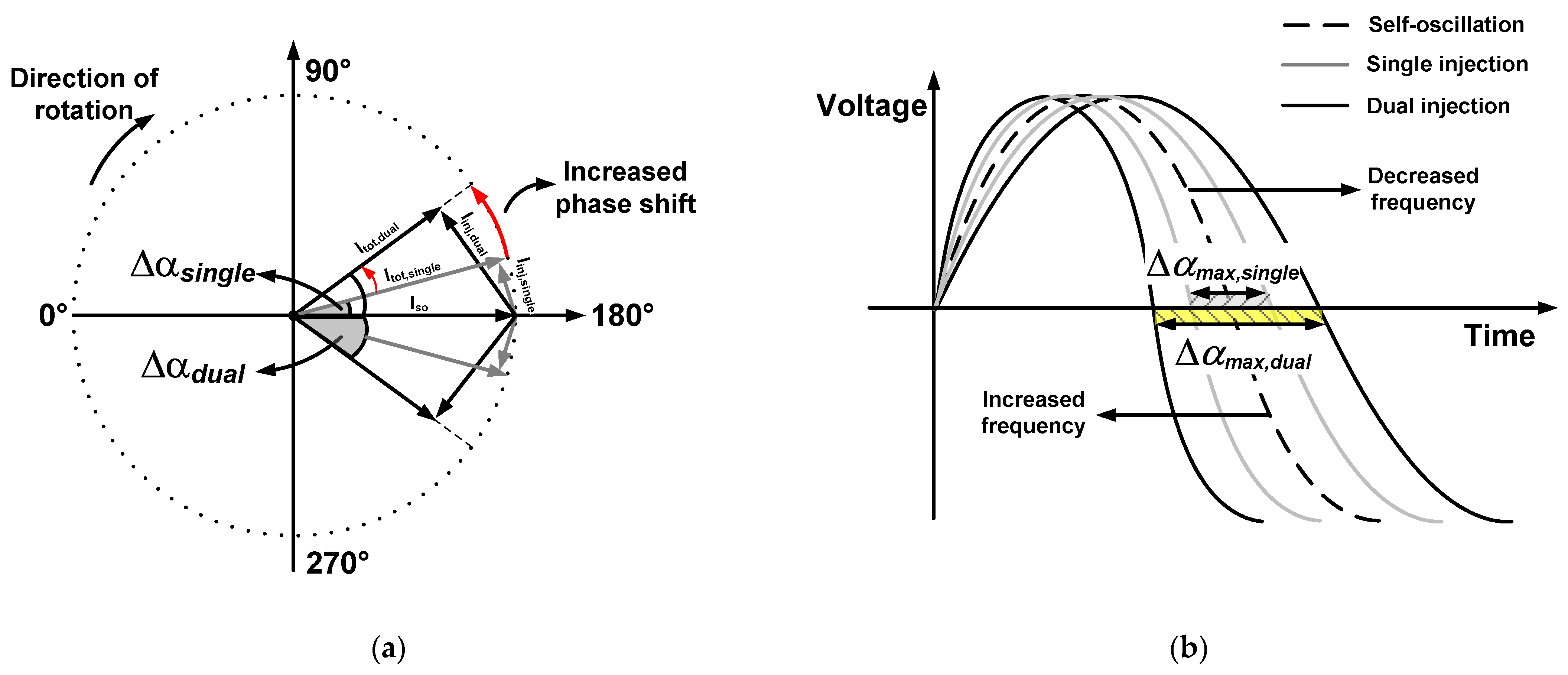
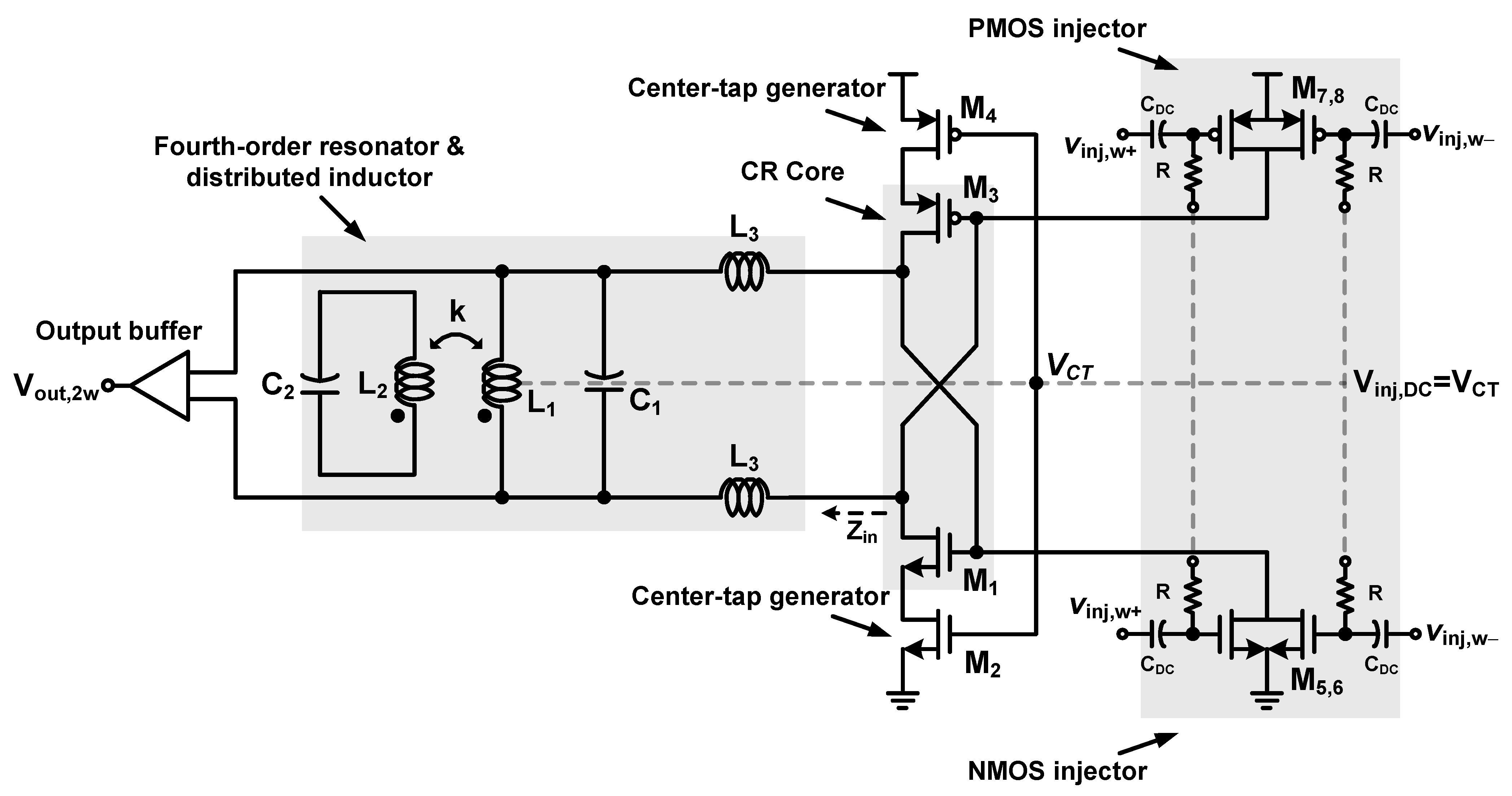
2.1. Dual Injection and Current-Reuse Core
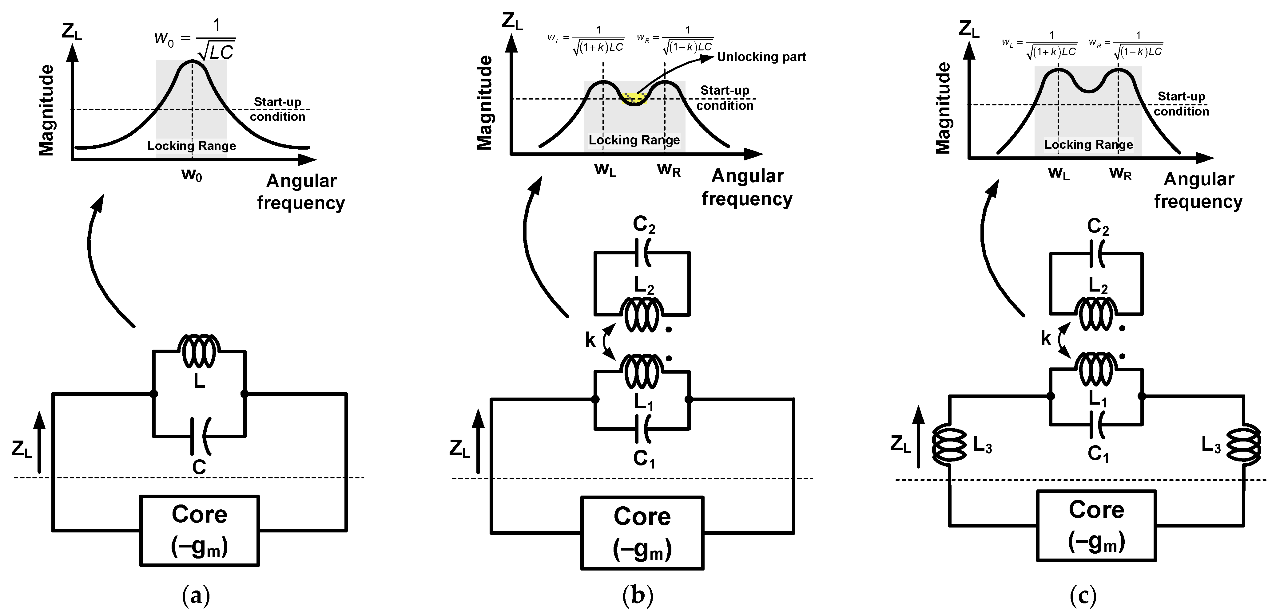
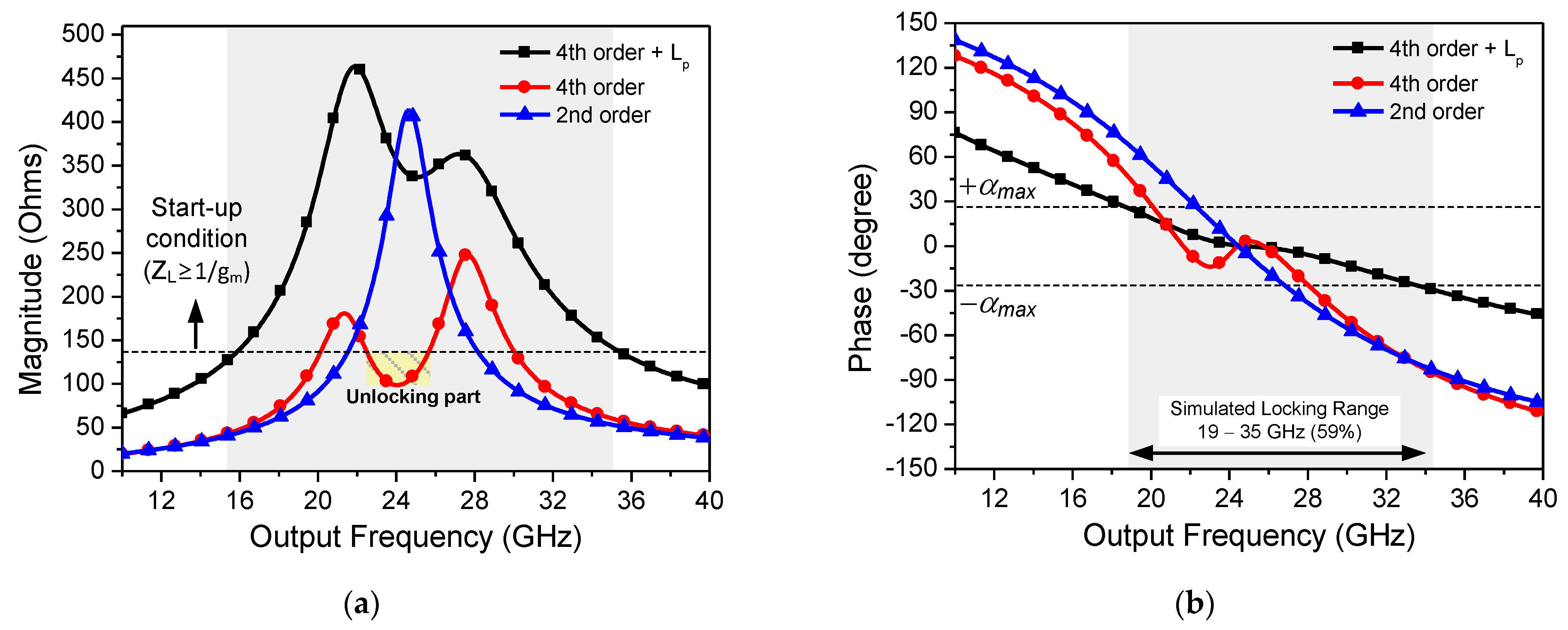
2.2. Fourth-Order Resonator
2.3. Proposed CR-ILFM
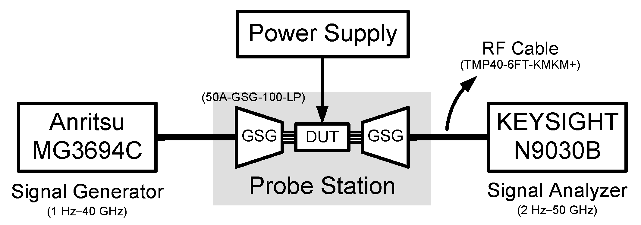
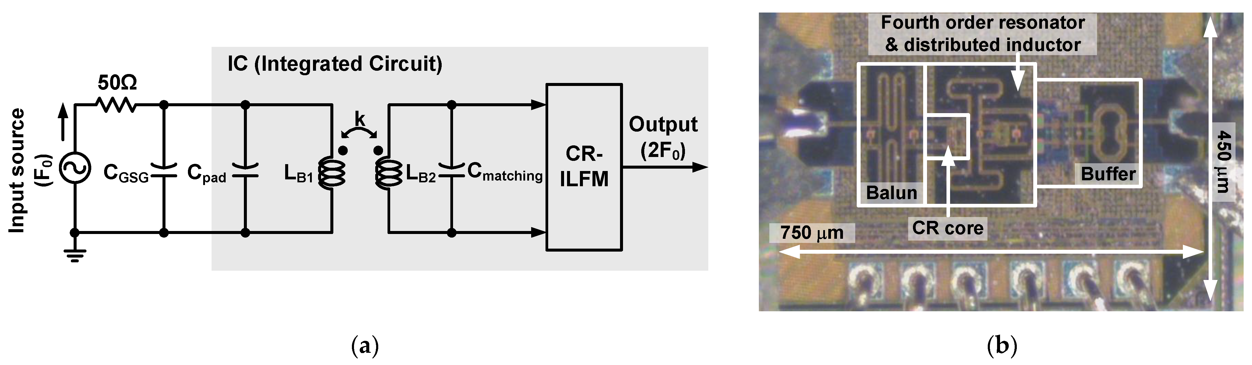
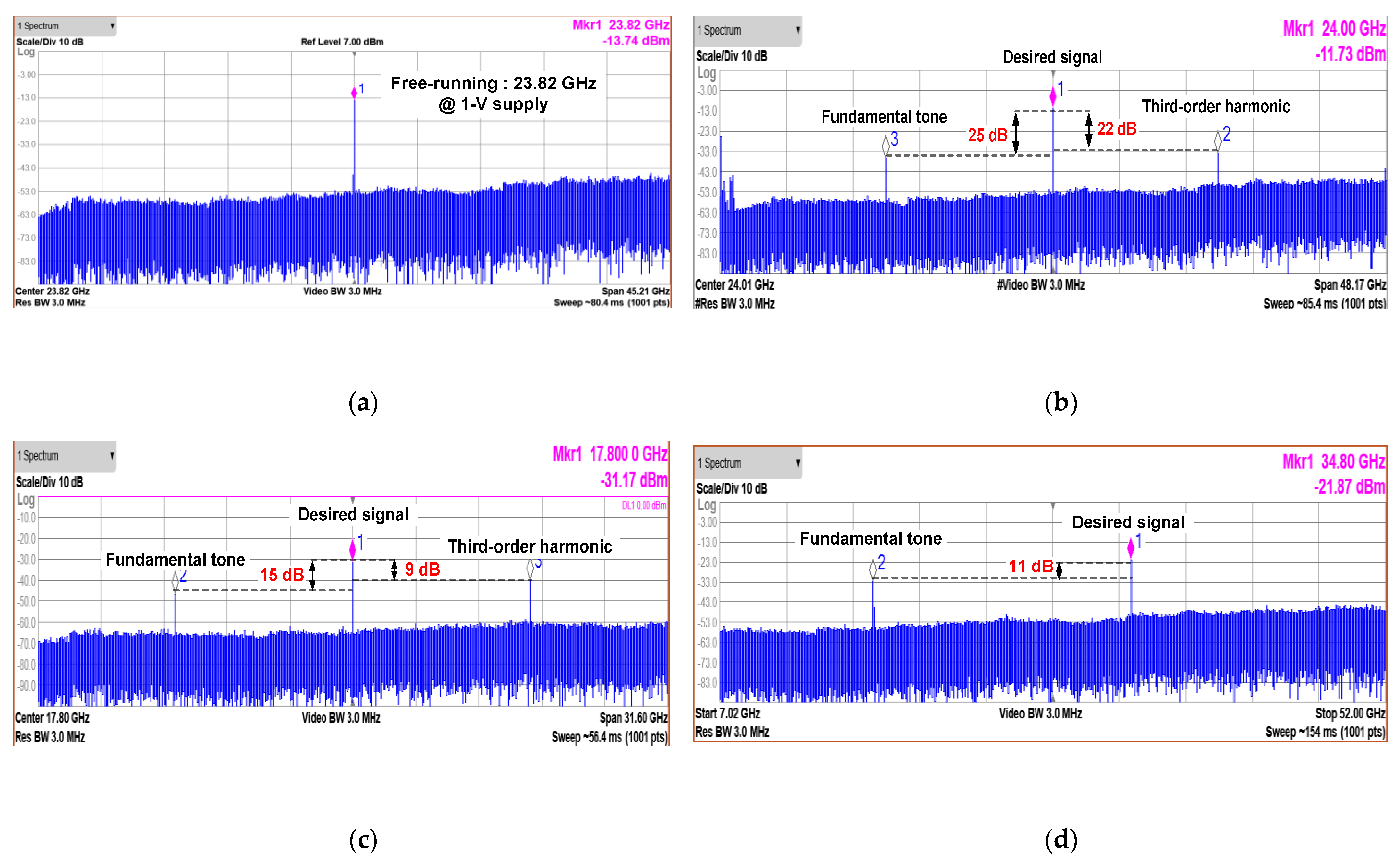
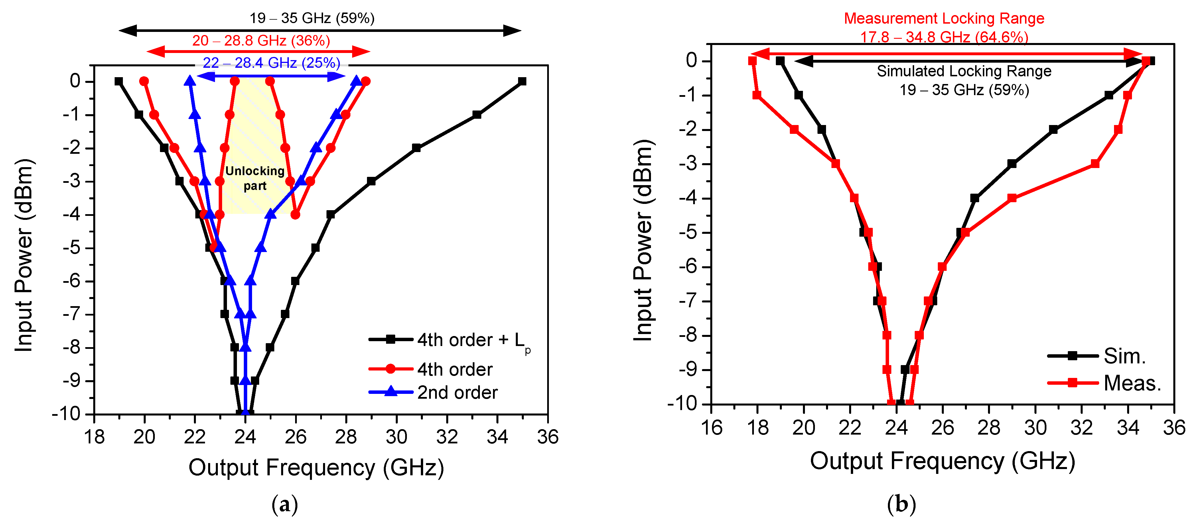
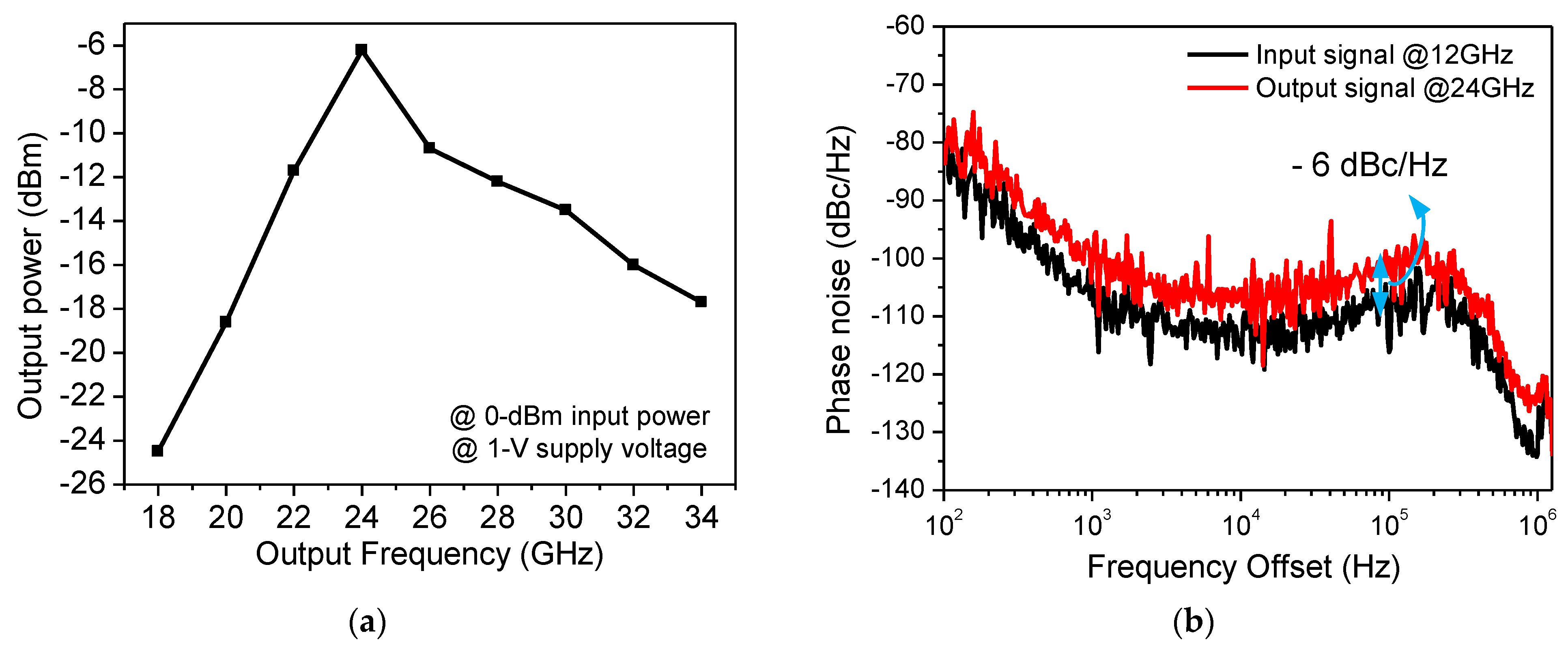
3. Measurement Results
4. Conclusions
Author Contributions
Funding
Acknowledgments
Conflicts of Interest
References
- Zhou, L.; Wang, C.-C.; Chen, Z.; Heydari, P. A W-band CMOS receiver chipset for millimeter-wave radiometer systems. IEEE J. Solid-State Circuits 2011, 46, 378–391. [Google Scholar] [CrossRef]
- Monaco, E.; Pozzoni, M.; Svelto, F.; Mazzanti, A. Injection-locked CMOS frequency doublers for μ-wave and mm-wave applications. IEEE J. Solid-State Circuits 2010, 45, 1565–1574. [Google Scholar] [CrossRef]
- Kim, H.-T.; Park, B.-S.; Song, S.-S.; Moon, T.-S.; Kim, S.-H.; Kim, J.-M.; Chang, J.-Y.; Ho, Y.-C. A 28-GHz CMOS Direct Conversion Transceiver with Packaged 2 × 4 Antenna Array for 5G Cellular System. IEEE J. Solid-State Circuits 2018, 53, 1245–1259. [Google Scholar] [CrossRef]
- Park, K.; Kim, D.; Lee, I.; Jeon, S. W-Band Injection-Locked Frequency Octupler Using a Push–Push Output Structure. IEEE Trans. Microw. Theory Tech. 2019, 29, 822–825. [Google Scholar] [CrossRef]
- Park, J.; Ryu, H.; Ha, K.-W.; Kim, J.-G.; Baek, D. 76–81-GHz CMOS Transmitter with a Phase-Locked-Loop-Based Multichirp Modulator for Automotive Radar. IEEE Trans. Microw. Theory Tech. 2015, 63, 1399–1408. [Google Scholar] [CrossRef]
- Mitomo, T.; Ono, N.; Hoshino, H.; Yoshihara, Y.; Watanabe, O.; Seto, I. A 77 GHz 90 nm CMOS Transceiver for FMCW Radar Applications. IEEE J. Solid-State Circuits 2010, 45, 928–937. [Google Scholar] [CrossRef]
- Lee, J.-Y.; Kim, G.S.; Ko, G.-H.; Oh, K.-I.; Park, J.G.; Baek, D. Low Phase Noise and Wide-Range Class-C VCO Using Auto-Adaptive Bias Technique. Electronics 2020, 9, 1290. [Google Scholar] [CrossRef]
- Yoo, S.; Choi, S.; Kim, J.; Yoon, H.; Lee, Y.; Choi, J. A Low-Integrated-Phase-Noise 27–30-GHz Injection-Locked Frequency Multiplier with an Ultra-Low-Power Frequency-Tracking Loop for mm-Wave-Band 5G Transceivers. IEEE J. Solid-State Circuits 2018, 53, 375–388. [Google Scholar] [CrossRef]
- Kang, C.-W.; Moon, H.; Yang, J.-R. Switched-Biasing Techniques for CMOS Voltage-Controlled Oscillator. Sensors 2021, 21, 316. [Google Scholar] [CrossRef]
- Li, S.; Chi, T.; Huang, T.-Y.; Huang, M.-Y.; Jung, D.; Wang, H. A Buffer-Less Wideband Frequency Doubler in 45-nm CMOS-SOI with Transistor Multiport Waveform Shaping Achieving 25% Drain Efficiency and 46–89 GHz Instantaneous Bandwidth. IEEE J. Solid-State Circuits Lett. 2019, 2, 25–28. [Google Scholar] [CrossRef]
- Shin, D.; Koh, K.-J. 24-GHz Injection-Locked Frequency Tripler with Third-Harmonic Quadrature Phase Generator. IEEE Trans. Circuits Syst. Ireg. Pap. 2019, 66, 2898–2906. [Google Scholar] [CrossRef]
- Shin, S.; Utomo, D.R.; Jung, H.; Han, S.-K.; Kim, J.; Lee, S.-G. Wide Locking-Range Frequency Multiplier by 1.5 Employing Quadrature Injection-Locked Frequency Tripler with Embedded Notch Filtering. IEEE Trans. Microw. Theory Tech. 2019, 67, 4791–4802. [Google Scholar] [CrossRef]
- Megawer, K.M.; Elkholy, A.; Coombs, D.; Ahmed, M.G.; Elmallah, A.; Hanumolu, P.K. A 5 GHz 370 fsrms 6.5 mW Clock Multiplier Using a Crystal-Oscillator Frequency Quadrupler in 65 nm CMOS. In Proceedings of the 2018 IEEE International Solid-State Circuits Conference (ISSCC) Digest of Technical Papers, San Francisco, CA, USA, 11–15 February 2018; pp. 392–394. [Google Scholar]
- Choi, S.; Yoo, S.; Choi, J. A 185 fsrms-Integrated-Jitter and −245 dB FOM PVT-Robust Ring-VCO-Based Injection-Locked Clock Multiplier with a Continuous Frequency-Tracking Loop Using a Replica-Delay Cell and a Dual-Edge Phase Detector. In Proceedings of the 2016 IEEE International Solid-State Circuits Conference (ISSCC) Digest of Technical Papers, San Francisco, CA, USA, 31 January–4 February 2016; pp. 194–196. [Google Scholar]
- Mazor, N.; Socher, E. Analysis and Design of an X-Band-to-W-Band CMOS Active Multiplier with Improved Harmonic Rejection. IEEE Trans. Microw. Theory Tech. 2013, 61, 1924–1933. [Google Scholar] [CrossRef]
- Jameson, S.; Socher, E. A 0.3 THz Radiating Active 27 Frequency Multiplier Chain with 1 mW Radiated Power in CMOS 65-nm. IEEE Trans. Terahertz Sci. Technol. 2015, 5, 645–648. [Google Scholar] [CrossRef]
- Lai, W.-C.; Jhuang, J.-W.; Jang, S.-L.; Lin, G.-Y.; Hsue, C.W. Wide-Band Injection-Locked Frequency Doubler. In Proceedings of the IEEE Asia Pacific Conference on Circuits and Systems, JEJU, Jeju Island, Korea, 25–28 October 2016; pp. 265–268. [Google Scholar]
- Zhang, J.; Liu, H.; Wu, Y.; Zhao, C.; Kang, K. An Injection-Current-Boosting Locking-Range Enhancement Technique for Ultra-Wideband mm-Wave Injection-Locked Frequency Triplers. IEEE Trans. Microw. Theory Tech. 2019, 67, 3174–3186. [Google Scholar] [CrossRef]
- Ha, K.-W.; Ryu, H.; Lee, J.-H.; Kim, J.-G.; Baek, D. Gm-Boosted Complementary Current-Reuse Colpitts VCO with Low Power and Low Phase Noise. IEEE Microw. Wirel. Compon. Lett. 2014, 24, 418–420. [Google Scholar] [CrossRef]
- Ha, K.-W.; Ryu, H.; Park, J.; Kim, J.-G.; Baek, D. Transformer-Based Current-Reuse Armstrong and Armstrong–Colpitts VCOs. IEEE Trans. Circuits Syst. Express Briefs 2014, 61, 676–680. [Google Scholar] [CrossRef]
- Ryu, H.; Ha, K.W.; Baek, D. Low-power quadrature voltage-controlled oscillator using current-reuse and transformer-based Armstrong topologies. Electron. Lett. 2016, 52, 462–464. [Google Scholar] [CrossRef]
- Yun, S.J.; Shin, S.-B.; Choi, H.-C.; Lee, S.-G. A 1 mW Current-Reuse CMOS Differential LC-VCO with Low Phase Noise. In Proceedings of the 2005 IEEE International Solid-State Circuits Conference (ISSCC) Digest of Technical Papers, San Francisco, CA, USA, 10 February 2005; pp. 540–541. [Google Scholar]
- Ha, K.-W.; Sung, E.-T.; Baek, D. Low-power transformer-based current-reuse injection-locked frequency divider. Electron. Lett. 2015, 51, 161–162. [Google Scholar] [CrossRef]
- Oh, K.-I.; Ko, G.-H.; Kim, J.-G.; Baek, D. An 18.8–33.9-GHz, 2.26-mW Current-Reuse Injection-Locked Frequency Divider for Radar Sensor Applications. Sensors 2021, 21, 2551. [Google Scholar] [CrossRef]
- Zhang, J.; Cheng, Y.; Zhao, C.; Wu, Y.; Kang, K. Analysis and Design of Ultra-Wideband mm-Wave Injection-Locked Frequency Dividers Using Transformer-Based High-Order Resonators. IEEE J. Solid-State Circuits 2018, 53, 2177–2189. [Google Scholar] [CrossRef]
- Li, A.; Zheng, S.; Yin, J.; Luo, X.; Luong, H.C. A 21–48 GHz Subharmonic Injection-Locked Fractional-N Frequency Synthesizer for Multiband Point-to-Point Backhaul Communications. IEEE J. Solid-State Circuits 2014, 49, 1785–1799. [Google Scholar] [CrossRef]
- Feng, P.-H.; Liu, S.-I. A Current-Reused Injection-Locked Frequency Multiplication/Division Circuit in 40-nm CMOS. IEEE Trans. Microw. Theory Tech. 2013, 61, 1523–1532. [Google Scholar] [CrossRef]
- Shin, D.; Koh, K.-J. An Injection Frequency-Locked Loop Autonomous Injection Frequency Tracking Loop with Phase Noise Self-Calibration for Power-Efficient mm-Wave Signal Sources. IEEE J. Solid-State Circuits 2018, 53, 825–838. [Google Scholar] [CrossRef]
- Chen, M.-C.; Wu, C.-Y. Design and Analysis of CMOS Subharmonic Injection-Locked Frequency Triplers. IEEE Trans. Microw. Theory Tech. 2008, 56, 1869–1878. [Google Scholar] [CrossRef]
- Bassi, M.; Boi, G.; Padovan, F.; Fritzin, J.; Martino, S.D.; Knauder, D.; Bevilacaqua, A. A 39-GHz Frequency Tripler with >40-dBc Harmonic Rejection for 5G Communication Systems in 28-nm Bulk CMOS. IEEE J. Solid-State Circuits Lett. 2019, 2, 107–110. [Google Scholar] [CrossRef]


| Design Parameter | Value |
|---|---|
| NMOS unit size (W/L) | 2 mm/0.06 mm |
| PMOS unit size (W/L) | 5 mm/0.06 mm |
| Finger of M1, M3 | 15 |
| Finger of M2, M4 | 50 |
| Finger of M5–M8 | 12 |
| L1 | 72 pH |
| L2 | 151 pH |
| L3 | 160 pH |
| k | 0.3 |
| C1 | 79 fF |
| C2 | 190 fF |
| This Work | [18] 19′MTT | [26] 14′JSSC | [8] 18′JSSC | [11] 19′TCAS1 | [27] 13′MTT | [28] 18′JSSC | [29] 08′MTT | [30] 19′JSSCL | ||
|---|---|---|---|---|---|---|---|---|---|---|
| Technology | 65-nm CMOS | 65-nm CMOS | 65-nm CMOS | 65-nm CMOS | 130-nm CMOS | 40-nm CMOS | 130-nm CMOS | 180-nm CMOS | 28-nm CMOS | |
| Core topology | CR-ILFM | ICB-ILFM | Sixth-order resonator- based ILFM | ILFM with frequency-tracking loop | HPS-ILFM | CR-ILFM | ILFM with frequency-tracking loop | Subharmonic ILFM | ILRO | |
| Self-oscillation frequency (GHz) | 23.82 | - | 28.1 | 29.25 | 24.44 | 50 | 30.1 | 26.49 | - | |
| Input signal power (dBm) | 0 | 0 | - ** | - | 0 | –5 | - ** | 4 | –6 | |
| Output freq. locking range | GHz | 17.8–34.8 | 22.8–43.2 ^ | 20.6–35.5 | 26.5–29.7 | 22.5–26.5 | 22.8–24.4 | 26.5–29.7 | 33.9–48.6 | 49.25–50.33 |
| % | 64.6 | 61.8 | 53.1 | 11.4 | 14.8 | 12.7 | 11.4 | 35 | 6.1 | |
| Output signal power (dBm) | −6.23 | −20 | −14.49 *** | - | −17 | −14.36 *** | −23.3 *** | −6.85 | 1 | |
| Phase noise (dBc/Hz) | At 100 kHz | −99.9@24 G | −94.7@28 G | −84.0@25.5 G | −92.6@29.3 G | −130@26.5 G | −110@24.45 G | −86.8@26.5 G | −122.5@39.6 G | - |
| At 1 MHz | −123.5@24 G | −114.0@28 G | −112.4@25.5 G | −115.6@29.3 G | −132@26.5 G | −115@24.45 G | −106.8@26.5 G | −126.5@39.6 G | −117.7@49.8 G | |
| Output phase type | Diff. | Diff. | Diff. | Quad. | Quad. | Diff. | Quad. | Diff. | Diff. | |
| Supply voltage (V) | 1 | 1.2 | 2.5 | 0.9–1.35 | 1.3 | 1.1 | 1.3 | 1.5 | 0.9 | |
| Total power consumption (mW) | 10.38 (7.48 *) | 14.8 (5.0 *) | 21.8 | 24.3 | 10.4 | (2.53 *) | 49.7 | 2.95 | 34 (25 *) | |
| FoM (%/mW) | 6.22 | 4.18 | 2.44 | 0.47 | 1.22 | 2.41 | 0.23 | 5.02 | 1.4 | |
| Chip size (mm2) | 0.75 × 0.45 | 0.67 × 0.70 | 1.85 × 1.13 ^^ | 0.85 × 0.55 | 0.5 × 0.25 † | 0.55 × 0.36 | 0.28 × 0.55 † | 0.66 × 0.69 | 0.1 mm2 | |
Publisher’s Note: MDPI stays neutral with regard to jurisdictional claims in published maps and institutional affiliations. |
© 2021 by the authors. Licensee MDPI, Basel, Switzerland. This article is an open access article distributed under the terms and conditions of the Creative Commons Attribution (CC BY) license (https://creativecommons.org/licenses/by/4.0/).
Share and Cite
Oh, K.-I.; Ko, G.-H.; Kim, G.-S.; Kim, J.-G.; Baek, D. A 17.8–34.8 GHz (64.6%) Locking Range Current-Reuse Injection-Locked Frequency Multiplier with Dual Injection Technique. Electronics 2021, 10, 1122. https://doi.org/10.3390/electronics10091122
Oh K-I, Ko G-H, Kim G-S, Kim J-G, Baek D. A 17.8–34.8 GHz (64.6%) Locking Range Current-Reuse Injection-Locked Frequency Multiplier with Dual Injection Technique. Electronics. 2021; 10(9):1122. https://doi.org/10.3390/electronics10091122
Chicago/Turabian StyleOh, Kwang-Il, Goo-Han Ko, Gwang-Sub Kim, Jeong-Geun Kim, and Donghyun Baek. 2021. "A 17.8–34.8 GHz (64.6%) Locking Range Current-Reuse Injection-Locked Frequency Multiplier with Dual Injection Technique" Electronics 10, no. 9: 1122. https://doi.org/10.3390/electronics10091122
APA StyleOh, K.-I., Ko, G.-H., Kim, G.-S., Kim, J.-G., & Baek, D. (2021). A 17.8–34.8 GHz (64.6%) Locking Range Current-Reuse Injection-Locked Frequency Multiplier with Dual Injection Technique. Electronics, 10(9), 1122. https://doi.org/10.3390/electronics10091122