1. Introduction
Technological advances in CMOS image sensors (CIS) have boosted their utilization in a variety of applications. In particular, CIS are widely employed in battery powered devices, such as smartphones or surveillance cameras, which have boosted interest in the design of low-power circuits to reduce battery consumption [
1,
2,
3,
4,
5]. At a system level, the effort to reduce power consumption has been conducted in various directions. For example, research has been focused on harvesting energy from the environment [
6,
7]; however, energy harvesting systems still require low-power CIS. Furthermore, readout circuits, including analog-to-digital converters (ADC) are usually power hungry, and a significant effort has been undertaken to reduce ADC consumption [
1,
3,
8]. Alternative readout schemes have been proposed to reduce power consumption [
9], while other analog encoding voltage techniques have been introduced to boost dynamic range (DR) [
10]. The need for high DR (HDR) imaging is mostly driven by automotive applications, where the light conditions can vary significantly [
11]. Alternative applications, such as scientific imaging, may benefit from an HDR sensor. Several approaches have been proposed to increase the DR [
12,
13,
14]. However, most of these solutions require a high number of samples, several transistors per pixel and/or computationally demanding post-processing. One candidate pixel architecture that combines HDR and low power is the logarithmic pixel, which exploits transistor subthreshold operation [
15,
16,
17]. Unfortunately, in low light conditions, their sensitivity to light is limited [
18] as in other CMOS pixels. The inherent high leakage current linked with CMOS processes is one of the principal causes of this degradation. This leakage current is also referred to as the “dark current” for its presence in the absence of light. The dark current is due to defects in the photodiode and at the boundaries and is mainly related to the manufacturing process. Therefore, the techniques to reduce the dark current also usually involve process modifications, generally by introducing either barriers to avoid the interaction with the source of the defects or by curing the defects, for example, with annealing [
19,
20,
21]. Unfortunately, any technique that involves process modification is costly to implement and is generally of limited availability to circuit designers. Other techniques based on circuit implementations have been presented. The dark current has been proven to be reduced by applying a negative offset operation on the gate of the transfer gate transistor [
22] or by clever layout techniques, which also improve the light response [
23,
24]. Furthermore, integrating CMOS Active Pixel Sensors have a limited dynamic range of 2–3 decades. This means that any significant improvement at the dark end of the response may lead to poor performance in the brighter regions. Therefore, an HDR sensor is required to fully utilize the advantages offered by reducing the dark current. A low dark current logarithmic pixel was previously reported [
25] where a theoretical analysis and simulation mismatch were conducted; however, no experimental evidence was provided. Experimental methods have been proposed to correct the mismatch in logarithmic pixels by modeling and calibration [
26]. In this paper, we report definitive proof of operation of a single, low, dark current pixel, which is manufactured in a CMOS technology and compared to a standard logarithmic pixel. The subthreshold logarithmic pixel architecture is intended for large formats and meets the needs of scientific imaging where low power, low dark current and wide dynamic range may be employed and where the demand of speed or pixel scaling is limited.
This paper is organized as follows. In
Section 2, we first present the physical foundation of our approach and the classic 3T logarithmic pixel. We also present the proposed approach with low voltage bias and enhanced low light operation.
Section 3 presents the experimental results, while
Section 4 concludes the paper.
2. Methodology
In CMOS image sensors, the dark current is mainly attributed to two different sources, in addition to any leakage due to surface or periphery defects. The first is the current injection–diffusion that originates from the random movement of carriers and depends on their concentration. The second is the thermal carrier generation–recombination described by the Shockley–Read–Hall equation for generation–recombination and directly depends on the applied voltage across the photodiode depletion layer. In CMOS pixels, the photodiode is usually operated in a reverse bias.
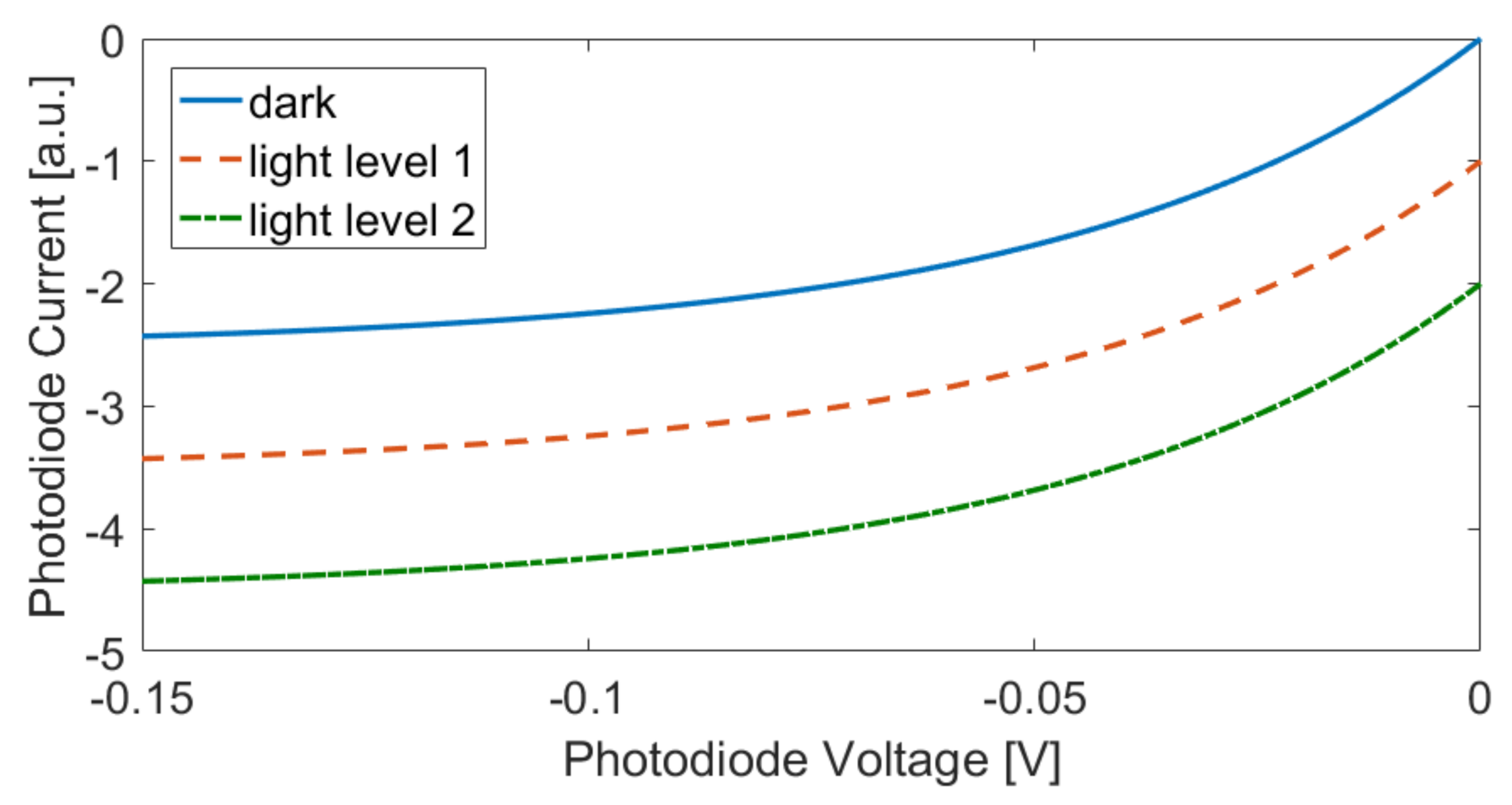
Figure 1 shows a simulated I-V characteristic of the photodiode at different light intensities and different bias voltages in a typical CMOS process. As can be observed in the figure, the photodiode leakage current is at its minimum value at a zero-voltage bias. When biased with a negative voltage, the dark current increases from this minimal value. Due to this, one may imagine that the dark current can be reduced if the photodiode operates as close as possible to zero volts. In this paper, we show that the logarithmic pixel can exploit a zero-volt operation, trading off against the use of additional transistors.
The strategy used to reduce the dark current is to keep the photodiode voltage close to zero. This is not possible using the standard Active Pixel Sensor, as it has limited dynamic range (DR). Hence, improving the dark current without enhancing the dynamic range will not fully exploit the high light region performance. A logarithmic pixel which converts the input photocurrent to an output logarithmic voltage is the optimum for single-frame recording, with the minimum number of transistors and limited post-processing required. Unfortunately, this pixel is worst affected by the dark current.
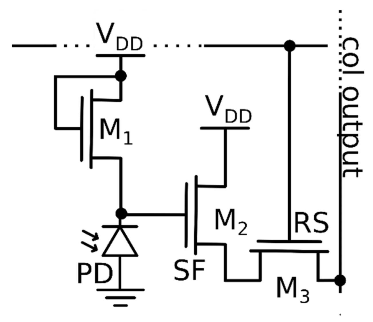
Figure 2 shows a typical logarithmic pixel where the nMOS load transistor
M1 is operating in the subthreshold region.
M2 and
M3 are the source follower (SF) and the row selector (RS), respectively, PD is the photodiode,
VDD is the supply voltage and col output is the column output node. The drain current of transistor
M1 is logarithmically related to the drain to source voltage as shown in Equation (1).
In Equation (1), VDD = VGM1 is the supply voltage, VTH is the threshold voltage, VT is the thermal voltage, IDS,M1 is the drain current flowing in M1, I0 is a characteristic current that defines the current that leaks through the transistor M1 and n is the subthreshold slope factor. Ideally, the output voltage is logarithmically proportional to the photogenerated current due to the incoming light. Unfortunately, the dark current produced in the photodiode gets added to the photogenerated current, limiting the sensitivity at the darker end of the pixel response. This effect also limits the gain sensitivity of the pixel. A possible solution to enhance the pixel response is to reduce the dark current. A circuit that implements this technique is presented in the next section.
It is worth noting that the main contribution of a photodiode dark current is related to the voltage applied across the photodiode as presented in
Figure 1. The typical bias voltage applied to the diode in a logarithmic pixel is similar to the pixel output. For example, the analogue supply voltage can be 3.3 V and hence, the output voltage is often comprised between 2.5 and 1.8 V, which generates a significant leakage contribution. A possible solution to reduce the dark current is to force a zero-potential difference across the photodiode. Such an approach is proposed in the pixel shown in
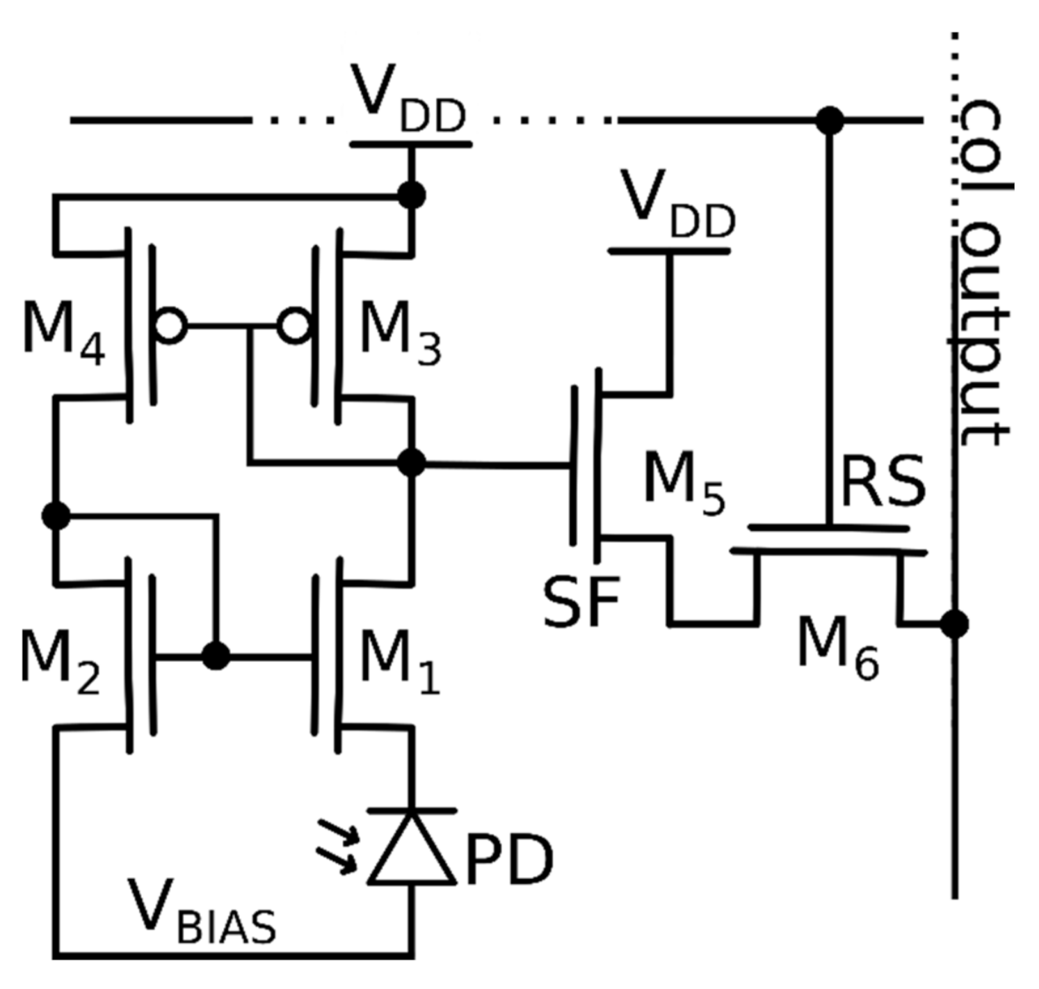
Figure 3. While in a standard logarithmic pixel, the output node is connected to the node biasing the photodiode; in the proposed circuit, this is split into two different nodes. In fact, this circuit is able to maintain a nearly zero potential across the photodiode, resulting in minimal leakage current, as the generation-recombination contribution to the dark current is close to zero. In this pixel, transistors
M3 and
M4 form a pMOS current mirror, and transistors
M2 and
M1 form a nMOS current mirror.
The output to the SF
M5 and to the readout circuitry is taken from the drain of the nMOS
M1, while the photodiode is connected to its source. In this pixel, the transistors are usually operating in subthreshold due to the low photocurrent produced in typical lighting conditions and the diode size used. The idea of the circuit is to copy the photogenerated current in the two branches of the circuit consisting of
M1,
M3 and
M2,
M4, respectively. When the same current flows in transistors
M1 and
M2, these will have the same gate-source voltage, in turn. The voltage drop on the photodiode can be expressed as the difference between the gate-source voltages of the nMOS couple
M2 and
M1 when considering the loop formed by the gate-source of the nMOS mirror pair and the photodiode, and can be written as follows:
where
VPD is the cathode-to-anode photodiode voltage and
VGS,M1 and
VGS,M2 are the gate-source voltages or the transistors
M1 and
M2, respectively. In turn, the source voltages depend on the biasing current of each pair and, for a subthreshold operating region, is expressed as follows:
where
VGS,Mx is the gate-source voltage of the transistors,
VTH is the threshold voltage,
VT is the thermal voltage,
IDS,Mx is the drain current flowing in either
M1 or
M2 and
IMx0 is a characteristic current that defines the current that leaks through transistors
M1 and
M2 and n is the subthreshold slope factor.
The top part of the circuit consists of a pMOS pair formed by identically sized transistors,
M3 and
M4, that replicate the current flowing in the right branch of the circuit into the left one, thereby achieving almost identical currents in both branches. The currents are almost identical, as we are not considering the mismatch of the devices in this analysis as it has been previously reported by the authors [
25]. In this case, if the drain-source currents are identical, the gate-source voltages should also be identical, thereby achieving a zero voltage drop across the photodiode. The current flowing in the branch is the sum of the photogenerated current and the dark current. When the photodiode is not exposed to light, only the dark current flows in the pixel. In this case, the output voltage is high; however, in the proposed pixel, this is the source of M
3, which is not directly connected to the photodiode as opposed to the logarithmic pixel. Thanks to this feature, the advantage of the proposed pixel compared to the typical logarithmic pixel is that the photodiode voltage is enforced to zero, thereby reducing the dark current. A lower dark current directly translates to a higher sensitivity at the darker end of the response, with a significant increase in the dynamic range in this portion of the pixel response.
The logarithmic response of the pixel is granted, thanks to the load transistor
M3, which is a diode-connected pMOS transistor. Equation (1) similarly applies and describes the output of the pixel, apart from the well-known differences between nMOS and pMOS transistors. The transistors
M5 and
M6 are the SF and the RS transistor, respectively. V
BIAS is the anode voltage of the photodiode. Depending on the process technology and the size of the transistors, this can either be connected to the ground or the bias voltage V
BIAS. In fact, let us consider the expression of the threshold voltage [
27]:
where
VFB is the flat-band voltage,
Na is the doping density in the substrate,
Cox is the gate oxide capacitance,
is the dielectric constant of the silicon,
q is the electron charge and ψ
B = (KT/q) log(Na/
ni) is the difference between the Fermi potential and the intrinsic potential in the substrate. A change of the body-source voltage will result in a variation of the threshold voltage. In the considered Equations (1)–(3), second-order effects have been ignored, and the change of V
TH should not affect the behavior of the current mirror. However, considering a more advanced expression of the subthreshold leakage [
28]:
where
IS is a factor that depends on the aspect ratio,
VTH0 is the zero bias threshold voltage, and
η is the Drain-Induced Barrier Lowering (DIBL) coefficient. For small values of
VBS, the body effect is linear and it is represented by the term
γ’
VS, where
γ’ is the linearized body effect coefficient. The subthreshold current is dependent on the
VDS voltage. In the double current mirror circuit, transistors
M1 and
M2 have different
VDS voltages. This difference causes a mismatch between the two I
DS currents. In turn, the mismatch between the currents causes the
VGS of the current mirror pair to be different, as well. This causes a voltage drop across the photodiode. However, increasing the
VBS voltage increases the effect of the first term in the exponential, compared to the second term where the
VDS is present. If sufficiently increased, the mismatch between the two currents will be reduced, and the photodiode voltage drop will be reduced as well. Alternatively, it is possible to increase the length of the transistor channels to minimize the DIBL effect. For the purpose of this paper, the transistor channel length was increased to 5 μm and the
VBIAS voltage was set to ground.
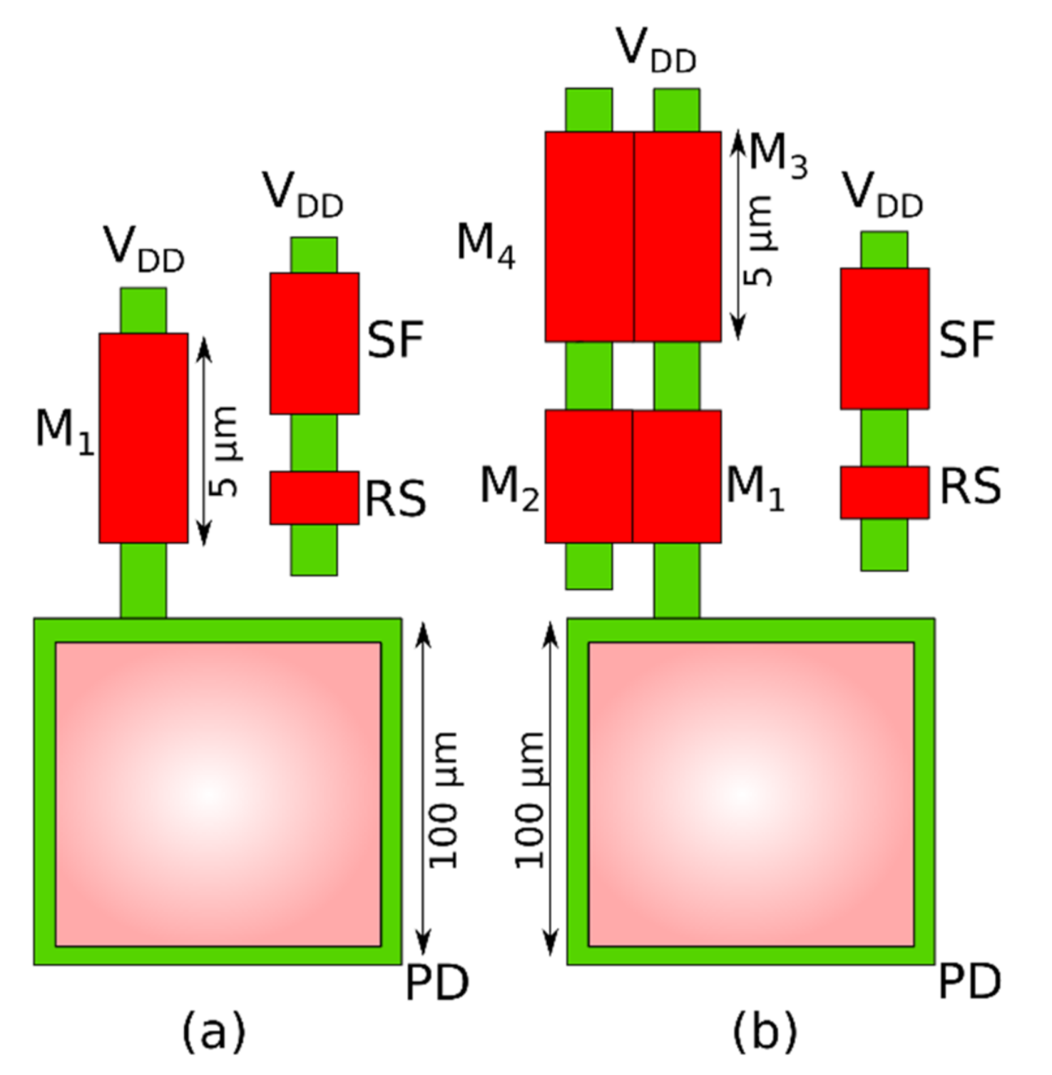
Figure 4 presents the pixel layout of the pixels that are compared in this study.
Figure 4a presents the layout of the logarithmic pixel, while
Figure 4b shows the layout of the proposed low dark current pixel. The load transistors,
M1 and
M3, have been designed with the same sizes, W = 5 μm, while their length is the minimum length allowed by the technology. The transistors are standard from the LFoundry CIS 110 nm PDK: low Vt 3.3 V MOS.
The chosen size of the photodiode (100 μm) does not allow a representation in-scale of the pixel. However, while in X-ray applications, large pixels are often utilized, in other applications, smaller pixels may be of interest. For this reason, we introduce a scaling model to estimate the fill factor achievable with the proposed design. Let us define p as the pixel pitch. The total area of the pixel can be then written as
Apix =
p2. To evaluate the fill factor, we need to evaluate the area of the photodiode. This can be estimated as the difference between the pixel area and the area occupied by the transistors
APD =
Apix −
Atr. The estimation of the area occupied by the transistors depends on the specific design considered and the design choices; however, for the case in this example, we can consider that the area of the SF and RS transistors is the same in both the logarithmic pixel and the proposed low dark current pixel. If the diffusion-to-diffusion minimum distance is also accounted for, it is possible to estimate the SF and RS area as 0.75 μm
2 (1.5 μm × 0.5 μm). In the logarithmic pixel, the load transistor
M1 area can be estimated as 2.75 μm
2 (5.5 μm × 0.5 μm), while in the proposed low dark current pixel, the core transistor area can be estimated as 11 μm
2 (5.5 μm × 0.5 μm × 4 transistors). Recalling the expression of the fill factor as the percent ratio between the photodiode area and the pixel area, it is possible to formalize the following:
where
APDlog and
APDldc are the areas of the logarithmic pixel photodiode and the low dark current pixel photodiode, respectively.
AM1 =
AM is the area of the load transistors and
ASF,RS is the area of the SF and RS transistors.
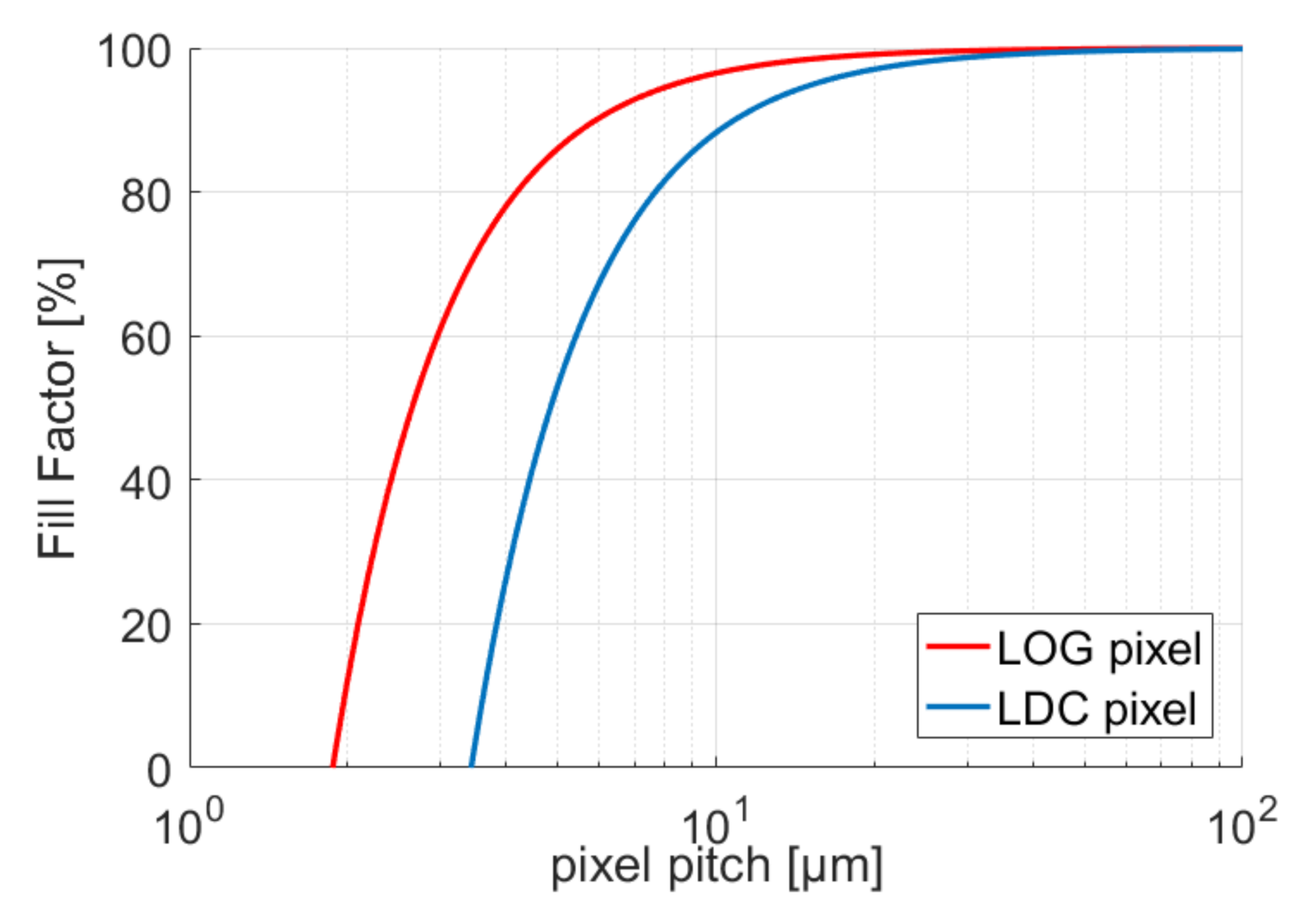
Figure 5 shows the calculated fill factor of Equations (6) and (7) for the logarithmic pixel and the proposed low dark current pixel, respectively. While for the pixel pitch of choice the difference is negligible, for smaller pixel pitches, the difference in fill factor increases. With LFoundry technology and the chosen transistor parameters, the achievable pixel pitch for the logarithmic pixel is smaller than the proposed low dark current pixel in front side illuminated technologies. However, for scientific applications, the typical pixel pitch is significatively larger, and for pitches above 20 μm, the difference can be neglected.
3. Experimental Results
This pixel was manufactured with LFoundry 110 nm Image Sensor process technology. It was implemented as a single device structure to prove functionality. In order to compare the proposed pixel with the standard logarithmic pixel, both versions have been designed and fabricated. Recalling
Figure 3, the load of the proposed pixel consists of a pMOS device. Therefore, the logarithmic pixel designed for this experiment also employs a pMOS as a load. In order to ensure a reliable comparison, both the standard and the proposed logarithmic pixels were connected to a photodiode of the same size (100 × 100 μm). Both were designed close in the die and exposed to the same light generated by a calibrated source during the measurements. The choice of a large pixel of 100 μm pitch also helps with the characterization. In fact, the typical dark current values nowadays in CIS are in the range of the pA/cm
2 and may be particularly difficult to measure. A larger photodiode provides a higher current, enabling measurements with common laboratory equipment.
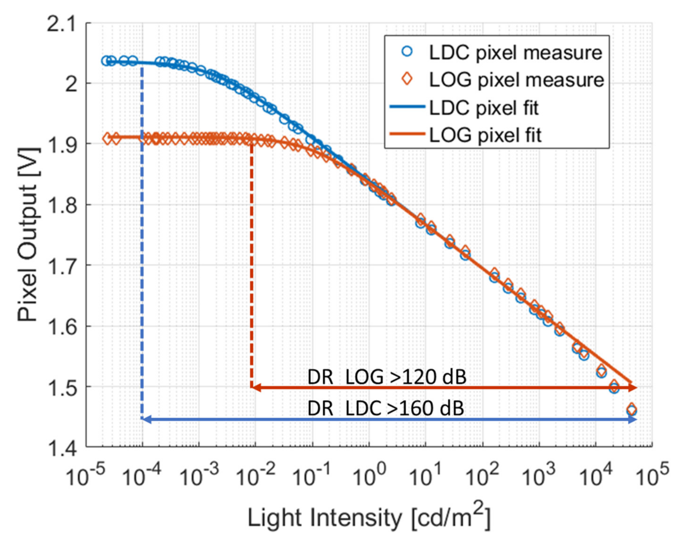
The pixels were measured in a laboratory environment where a calibrated light source was used to shine the light through an integrating sphere to guarantee uniformity. The measurement setup was equipped with a high sensitivity photodiode. The measurement results are shown in
Figure 6, where the pixel output voltages are plotted against the measured incoming light intensity. The red diamonds represent the response of the standard logarithmic pixel, while the blue circles represent the response of the proposed low dark current pixel. In addition, the data were fitted with the model presented in Equation (8) in order to estimate the dark current levels. Equation (8) is a model for Equation (1), where the dark current has been made explicit and the parameters simplified, resulting in the following [
10]:
where
a is the offset,
b is the gain and
c is the dark current contribution of each pixel. The terms
a and
b are characteristic parameters, depending on the process, temperature and to the readout circuitry. In this experiment, the measurements were conducted at the same temperature and with the same process technology. Therefore, the aforementioned parameters are expected to be similar for both pixels. However, the c-terms are different, as they represent the different levels of the dark current, which, in turn, depend on the bias voltage of the photodiode. Let us define c
log and c
ldc, the dark current terms for the logarithmic and low dark current pixel, respectively. The ratio between the c terms represents the dark current reduction rate. The measured ratio is c
ldc/c
log = −34.54 dB, which corresponds to a reduction in the dark current by a factor higher than 50. In addition, we can analyze the slope of the pixel responses to determine their sensitivity.
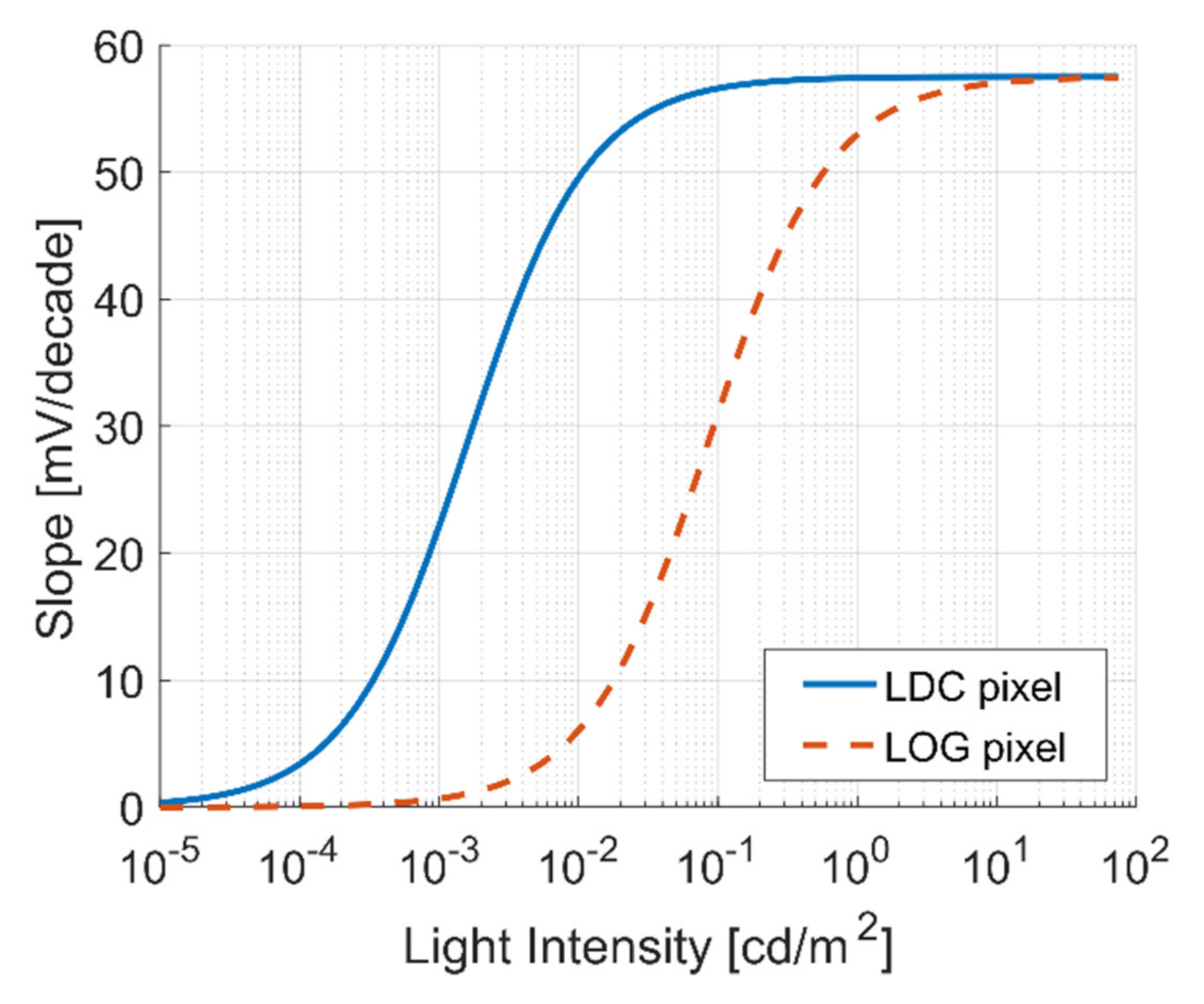
Figure 7 shows the slopes of both the logarithmic and low dark current pixels.
The slope represents the sensitivity of the pixel as a function of the input light intensity. From this figure, the low dark current pixel exhibits a higher sensitivity for lower values of incoming light compared to the logarithmic pixel. In their normal region of operation, both pixels have a slope of 58 mV/decade. Furthermore, this is guaranteed for a higher range in the proposed pixel. From the analysis conducted in this paper, it is possible to conclude that the proposed low dark current pixel circuit has a wider dynamic range of ~35 dB at the darker end of the response compared to a logarithmic pixel. The results are summarized in
Table 1.
