Article

Hybrid Memristor–CMOS Implementation of Combinational Logic Based on X-MRL †

1
IMT Atlantique, Lab-STICC CNRS, UMR, 29238 Brest, France
2
Lebanese International University, School of Engineering, Block F 146404 Mazraa, Beirut 146404, Lebanon
3
Faculty of Sciences, Lebanese University, Beirut 6573, Lebanon
4
IRL CROSSING CNRS, Adelaide 5005, Australia
*
Author to whom correspondence should be addressed.
This paper is an extended version of our paper published in IEEE International Conference on Electronics, Circuits and Systems (ICECS), 27–29 November 2019, as Ali, K.A.; Rizk, M.; Baghdadi, A.; Diguet, J.P.; Jomaah, J. “MRL Crossbar-Based Full Adder Design”.
Electronics 2021, 10(9), 1018; https://doi.org/10.3390/electronics10091018
Submission received: 22 February 2021 / Revised: 15 April 2021 / Accepted: 18 April 2021 / Published: 24 April 2021
(This article belongs to the Section Circuit and Signal Processing)

Abstract

:
A great deal of effort has recently been devoted to extending the usage of memristor technology from memory to computing. Memristor-based logic design is an emerging concept that targets efficient computing systems. Several logic families have evolved, each with different attributes. Memristor Ratioed Logic (MRL) has been recently introduced as a hybrid memristor–CMOS logic family. MRL requires an efficient design strategy that takes into consideration the implementation phase. This paper presents a novel MRL-based crossbar design: X-MRL. The proposed structure combines the density and scalability attributes of memristive crossbar arrays and the opportunity of their implementation at the top of CMOS layer. The evaluation of the proposed approach is performed through the design of an X-MRL-based full adder. The design is presented with its layout and corresponding simulation results using the Cadence Virtuoso toolset and CMOS 65 nm process. The comparison with a pure CMOS implementation is promising in terms of the area, as our approach exhibits a 44.79% area reduction. Moreover, the combined Energy.Delay metric demonstrates a significant improvement (between × 5.7 and × 31 ) with respect to the available literature.

1. Introduction

The memristor is the fourth fundamental circuit element, which relates charge and magnetic flux linkage. It was originally predicted by Professor Leon Chua in 1971 [1]. The memristor was realized later by members of HP Labs in 2008 [2]. This successful realization opened a wide area of research on the memristor and its possible applications. The HP memristor is a solid state device formed of a nanometer scale TiO 2 thin film, containing a doped and an undoped region sandwiched between two platinum electrodes. The obtained two-terminal device exhibits a dynamic resistance that is bounded between a minimum value ( R O N ) and a maximum value ( R O F F ). Its resistance depends on the magnitude, direction and duration of the applied voltage across its terminals. The last attained resistance value of the memristor before withdrawing the applied voltage is naturally retained. Memristors are promising in the field of non-volatile memories (NVM) because of their capability for data retention [3] with zero standby power and compatibility with a conventional CMOS in terms of fabrication and operating voltages. Due to their versatile nature, the use of memristors has been extended from memory to computing [4]. Several memristive logic design families have emerged in the literature, each with its own characteristics, capabilities and usage. Memristor Aided Logic (MAGIC) [5] and the Material Implication (IMPLY) [6] are considered as memristive stateful logic families [7]. They were introduced to allow logic computations inside memristive memory systems and are being explored to overcome the memory wall problem. Memristor-Ratioed Logic (MRL) [8] is another memristor-based logic design style. MRL is a hybrid memristor–CMOS logic family. Its goal is to implement conventional combinational logic circuits, which are the building block of digital systems [8,9,10,11]. The main idea behind MRL is to replace as many transistors with nano-scale size memristors as possible while keeping the role of the intended digital architecture the same.
Of the above-mentioned logic design styles, MRL is the only approach that matches the conventional CMOS in terms of the adopted state variable. Both MRL and the CMOS use voltage as the only state variable to represent inputs and outputs throughout all intermediate stages. Thus, MRL is the most qualified for integration in current CMOS designs. However, this integration should be performed in a way that efficiently exploits the promising characteristics of memristive devices, such as density and scalability. This can be achieved through the use of the crossbar structure, which is a highly adapted topology for arranging memristors at the top of the CMOS layer.
In this paper, we propose an MRL-based crossbar design: X-MRL. X-MRL is intended for implementing combinational logic. The conventional CMOS logic gates are implemented using MRL, and an original mapping into a crossbar structure is proposed. The proposed methodology efficiently combines the density and scalability attributes of crossbar arrays and the ability to implement memristors at the top of the CMOS layer. The proposed approach is evaluated by designing an X-MRL-based full adder circuit [12]. The designed architecture is implemented and simulated with the Cadence Virtuoso toolset.
The rest of the paper is organized as follows. Section 2 describes the behavior of the memristor and the corresponding available models. Section 3 presents a brief review of the MRL design style. Section 4 presents the proposed X-MRL design for realizing Boolean computation. Section 5 provides and discusses the simulation results and performance analysis. A comparison with previous published designs is presented in Section 6. Finally, Section 7 concludes the paper.

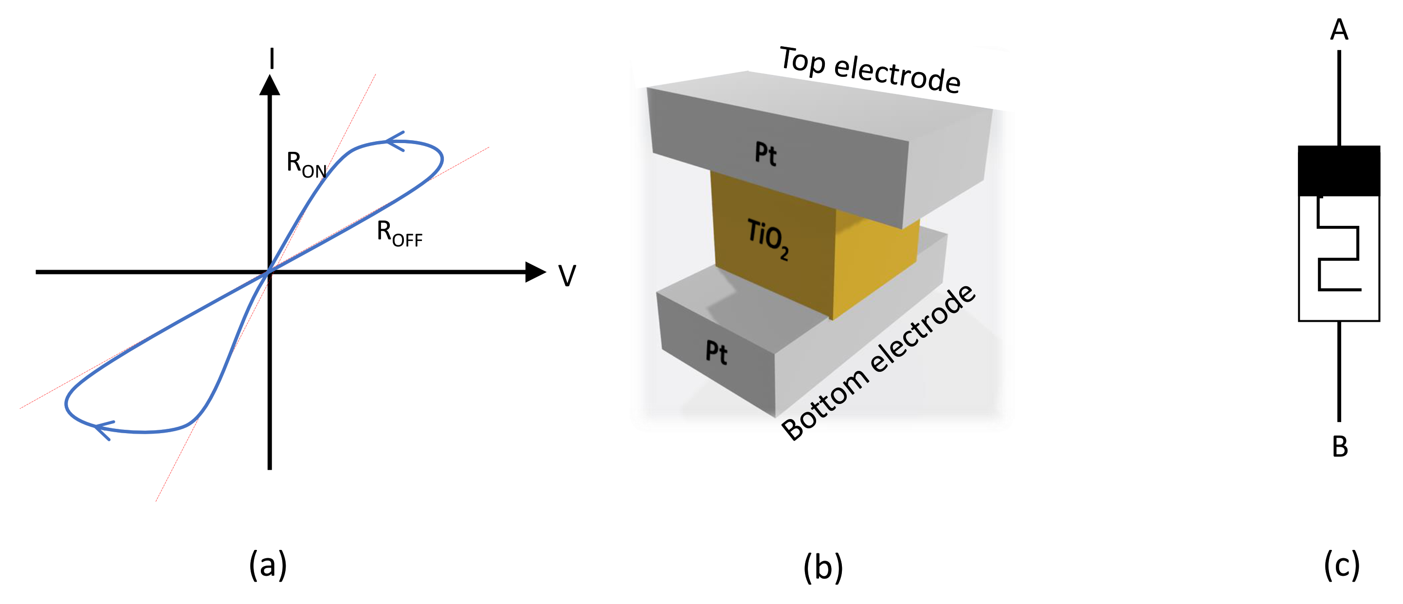
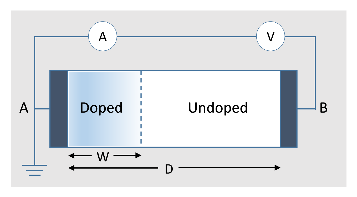
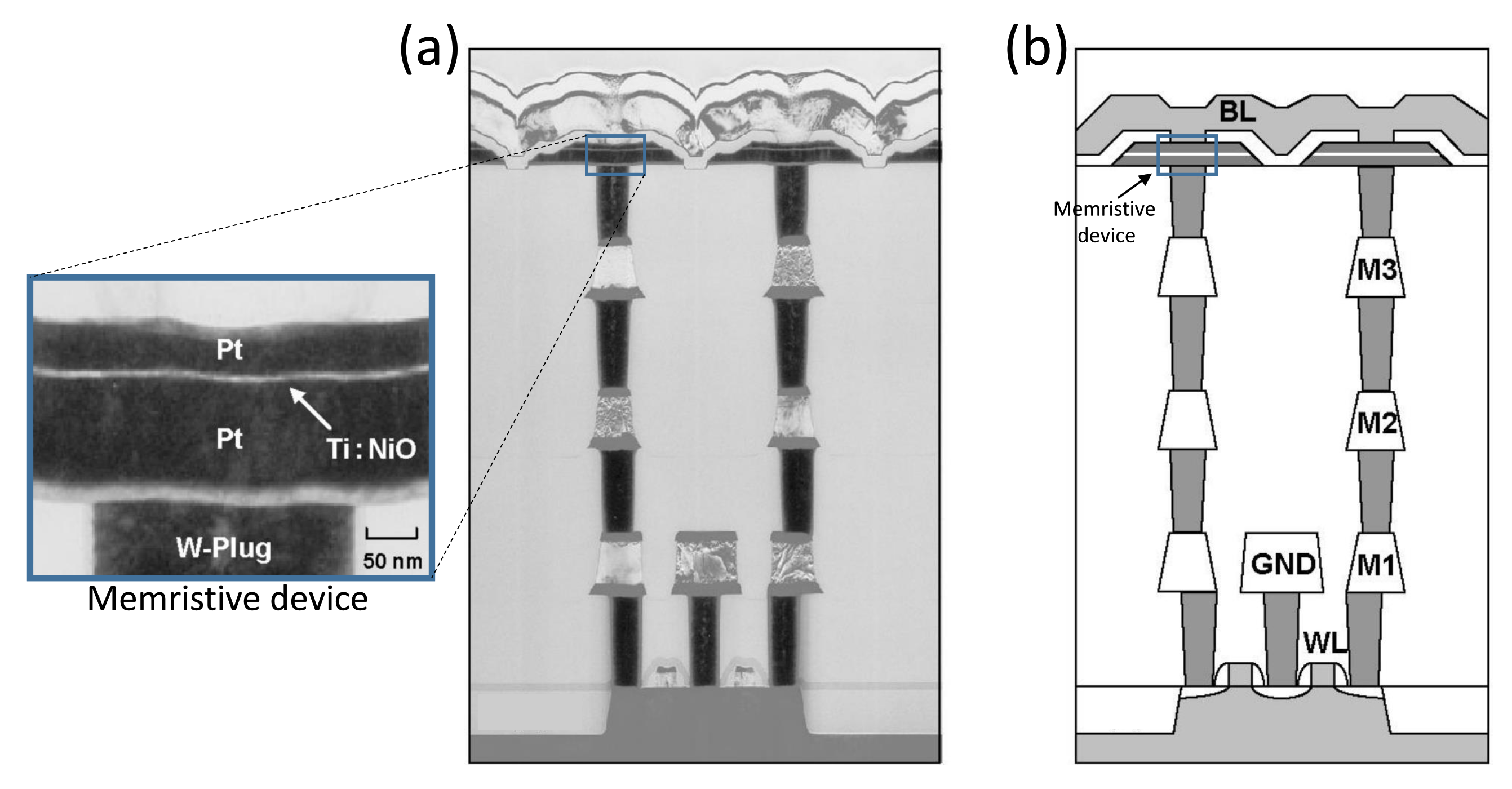
2. Memristor Behavior and Modeling

Chua [1] has defined the memristor as a previously missing relation between the flux ϕ and the charge q, yielding the defining relation
M ( q ) = d Φ / d q
The current–voltage (I-V) characteristic of a memristor has the form of a pinched hysteresis loop, as illustrated in Figure 1a. The hysteresis phenomenon indicates that memristor resistance could be modulated between two resistance states R O N and R O F F . Figure 1b schematizes the 3D structure of the memristor device, and Figure 1c depicts the typically used symbol to represent a single memristor. HP Labs has described the physical model of a memristor as shown in Figure 2; it consists of two layers of TiO 2 sandwiched between platinum contacts [2]. One of the TiO 2 layers is doped with oxygen vacancies, while the other is left undoped. As a result, the doped region behaves as a semiconductor while the undoped region behaves as an insulator.
The width of the doped region w ( t ) varies between zero and a memristor length of D according to the amount and direction of the electric charges q ( t ) moving across the memristor. Thus, applying a certain bias to the memristor leads to the flow of current, which in turn changes the value of w ( t ) . Therefore, the virtual boundary separating the doped and undoped regions moves, leading to a variation in the memristor’s total resistance R M E M as expressed in Equation (2) [2].
R M E M ( x ) = R O N ( x ) + R O F F ( 1 x )
where x = w D [ 0 , 1 ] and R O N and R O F F are the limiting values of memristor resistance when w = D and w = 0 , respectively. The speed of the boundary movement between the two ends is called the drift velocity and is represented by the state equation [2]
d x d t = k i ( t ) f o r k = μ v R O N D 2
where μ v is the dopant mobility. Equation (3) considers that the drift velocity is constant, resulting in a linear drift model of the memristor. However, the experiments presented in [13,14] proved that the behavior of the implemented memristor is non-linear. To manage the issue of nonlinearity, several models have been proposed in the literature. In [14], the authors proposed a non-linear dopant drift model as a relation between the current and voltage (I-V) of the memristor. In [15], the drift velocity was expressed using a window function f ( w ) in order to model the non-linearity, as expressed in Equation (4).
d w d t = a f ( w ) V ( t ) m
where a and m are constants, f ( w ) is the window function and m is an odd integer. The previous presented models are based on the HP physical representation of a memristor. In [13], Pickett et al. proposed a more accurate physical model of a memristor. A resistor is connected in series with an electron Simmons tunnel barrier [16] instead of connecting two resistors in series, as demonstrated in HP’s model. This model exhibits non-linear and asymmetric switching characteristics. Its state equation is expressed in Equation (5):
d x d t = C o f f sinh i i o f f exp exp x a o f f w c | i | b x w c C o n s i n h i i o n exp exp x a o n w c | i | b x w c
where the state variable x represents the width of the Simmons tunnel barrier, C o f f , C o n , a o f f , a o n , w c and b are the fitting parameters, and i o f f and i o n are the current thresholds of the memristor. Obviously, Equation (5) shows that the Simmons tunnel barrier model is more complicated; thus, it is computationally inefficient. In order to attain a simplified and general model, Kvatinsky et al. [17] presented the TEAM model, which represents in simpler expressions the same physical model as the Simmons tunnel barrier model. Equation (6) expresses the state equation representing the TEAM model:
d x d t = K o f f i ( t ) i o f f 1 α o f f f o f f ( x ) , 0 < i o f f < i K o n i ( t ) i o n 1 α o n f o n ( x ) , i < i o n < 0 0 otherwise
where i o n and i o f f are the current thresholds of the memristor. K o n , K o f f , α o n and α o f f are fitting parameters, and f o n ( x ) and f o f f ( x ) are the corresponding window functions of the memristor. However, experimental data acquired from several memristive devices reveal the existence of a voltage threshold rather than a current threshold [18]. In [18], the TEAM model was extended to the VTEAM model. Equation (7) describes the VTEAM model. It is similar to the expression in Equation (6), except for the voltage dependence v ( t ) and the respective SET and RESET voltage thresholds v o n and v o f f . Moreover, the VTEAM model is considered as a general model since it can be fitted to any other memristor model [18].
d x d t = K o f f v ( t ) v o f f 1 α o f f f o f f ( x ) , 0 < v o f f < v K o n v ( t ) v o n 1 α o n f o n ( x ) , v < v o n < 0 0 otherwise
Normally, the window function f ( x ) is added for a memristor model in order to decelerate the moving boundary of the memristor before reaching its extremities and to guarantee a zero speed exactly when it reaches either one of them. In this study, we have adopted the VTEAM model to describe the simulated memristor as it provides simple and realistic modeling.

3. Memristor-Based Logic Design Styles

In the literature, three main design styles for using memristors in logic design can be found. The first two design styles, which are IMPLY [6,19] and MAGIC [5], exploit only memristors for logic implementations. The third design style, known as MRL [8], adopts a combination of CMOS and memristor devices. This section presents a brief overview of these design styles.

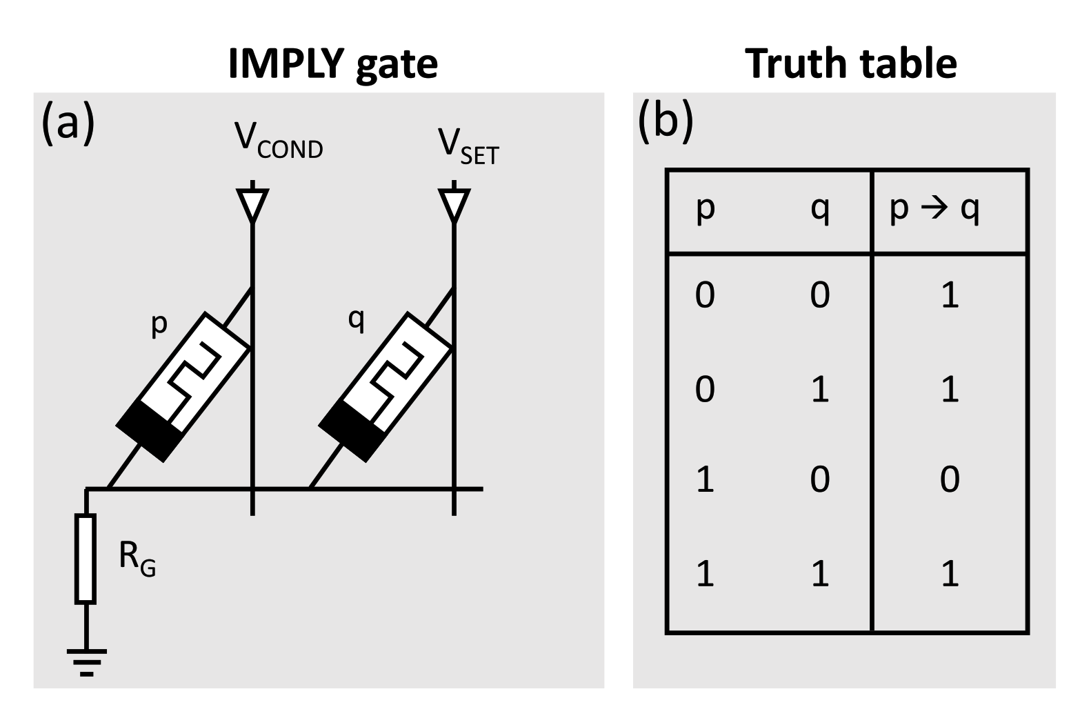
3.1. Material Implication IMPLY Gates

In IMPLY, the memristor states ( R O F F , R O N ) represent the logical state variables (0, 1), respectively. As shown in Figure 3a, the gate consists of the two memristors p and q and the resistor R G . The initial memristances of p and q represent the input to the gate, while the output is written into memristor q after applying V C O N D and V S E T simultaneously. The truth table of the IMPLY gate is shown in Figure 3b, where p q = p + q can be used as a basis for any logic function. As a result, the same memristors are used to store the logical state and/or perform a logical operation. Consequently, the computation requires several sequential operations. Several approaches have been proposed in the literature that adopt IMPLY for the execution of combinational logic [6,20,21]. All available designs require several time steps to accomplish the target computations. This fact leads to an overhead in terms of time delay compared to other logic implementation techniques.

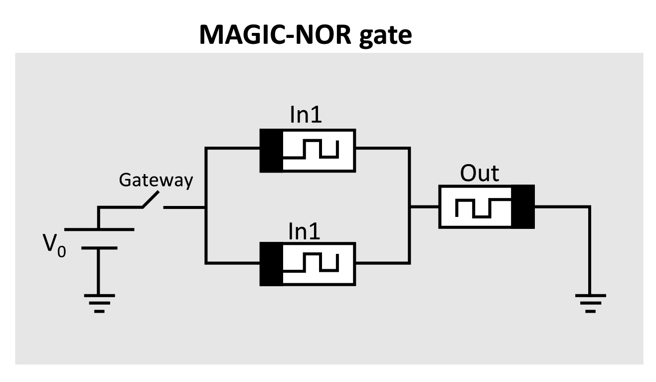
3.2. Memristor Aided Logic (MAGIC)

MAGIC is a memristor-only logic design style that supports Boolean functions [5]. Unlike IMPLY, this logic family makes use of separate memristors to store the input bits, and an additional memristor is used to store the output bit. Figure 4 illustrates the 2NOR1 MAGIC gate where i n 1 and i n 2 serve as the input memristor and o u t serves as the output memristor. The logic state in MAGIC implementation is represented by the resistance stored in the utilized memristors, where R O F F and R O N represent logic “0” and logic “1”, respectively. Thus, when driving the gate with voltage V 0 , the result of the NOR operation of i n 1 and i n 2 is written simultaneously into o u t .
Applications of MAGIC in memristor-based crossbars are straightforward when using MAGIC NOR, while an additional resistor is required in case of other gates. The authors of [22,23,24] used the MAGIC NOR as the basis to perform logic computation inside the memory, thus adding processing capabilities. In other words, each processing task is divided into a sequence of MAGIC NOR operations, which are executed one after the other using the memory cells as computation elements.

3.3. Memristor Ratioed Logic (MRL)

The third design style of memristor-based logic is Memristor Ratioed Logic (MRL) [8]. It is a typical hybrid CMOS–memristor logic design where the programmable resistance of memristors is exploited in the computation of the Boolean AND and OR functions. MRL opts for voltage as the state variable, in a similar manner to CMOS-based devices; thus, the computation is accomplished in a single step. This criterion eliminates the drawbacks of the sequential process of IMPLY logic devices. Figure 5 depicts the structures of the MRL AND, NAND, OR and NOR gates. Both OR and AND gates consist of two anti-serial memristors (i.e., connected serially with opposite polarities), whereas for NOR and NAND, a CMOS inverter is added at the output.
Both MRL AND and OR gates react similarly when identical values are set to their input ports (when both inputs are set either to logic “1” or “0”). In this case, no current flows through the anti-serial memristors, leading to the transfer of the input voltage to the output. In the case where different values are set to the input ports (i.e., the first port is set to “0” and the second port is set to “1”, or vice versa), a current flows from the port with higher potential (logic “1”) to the port with lower potential (logic “0”). The resulting potential difference changes the internal state of both memristors in an opposite manner. One memristor tends to attain the R O N state while the other tends to attain the R O F F state. In addition, the connected memristors form the well-known voltage divider circuit. Assuming R O F F > > R O N , Equations (8) and (9) present the obtained output values V o u t of MRL OR and AND gates, respectively [8].
V o u t , O R = ( R O F F R O F F + R O N ) × V C C V C C
V o u t , A N D = ( R O N R O N + R O F F ) × V C C 0
Note that the output voltage V o u t converges to the higher potential (logic “1”) in the MRL AND gate and to the lower potential (logic “0”) in the MRL OR gate. Figure 6 illustrates the logical operations of the MRL AND gate corresponding to all input combinations.
However, cascading several MRL gates leads to a floating output (between logic “0” and logic “1”) due to voltage degradation [8]. Since memristors are passive devices, they cannot amplify signals. Therefore, CMOS inverters can be used as buffers after several stages to restore the attained logical state [8].
Several recent research works presented in the literature exploit the use of MRL to design basic building blocks. In [8], a design dedicated to a universal full adder circuit was proposed using MRL gates with the aid of CMOS inverters instead of pure CMOS-based gates. In [25], the authors demonstrated a simple circuit based on MRL which is capable of executing AND, OR and XOR in parallel. The design is considered to be hybrid. However, cascading several stages of this circuit degrades its performance due to the voltage drop at the output. In [11], the authors presented an implementation strategy for a memristor-based Programmable Logic Array (PLA). The memristor-based circuit transformation of PLA is based on MRL gates. However, the arrangement of memristors at the top of the CMOS layer and the corresponding layout were not investigated by the authors.

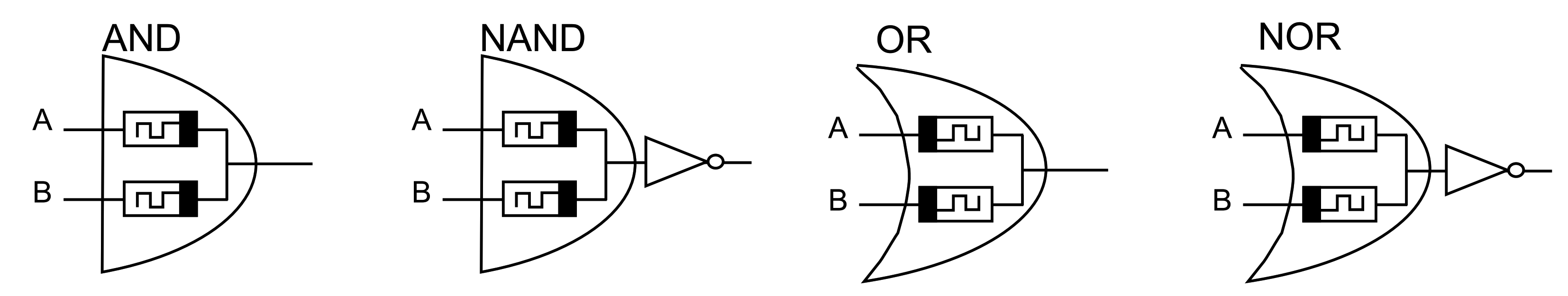
4. Proposed X-MRL Design for Logic Computation

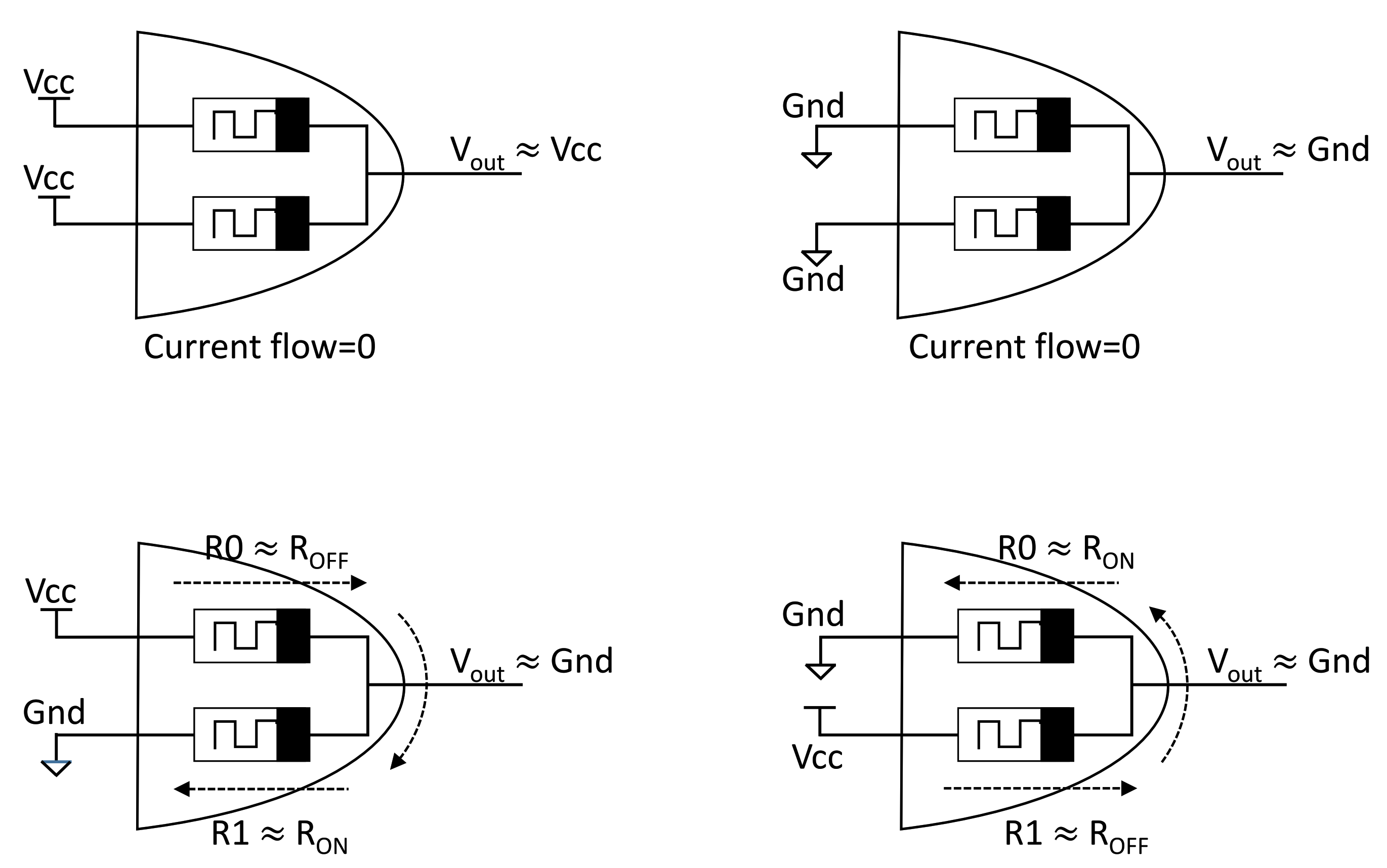
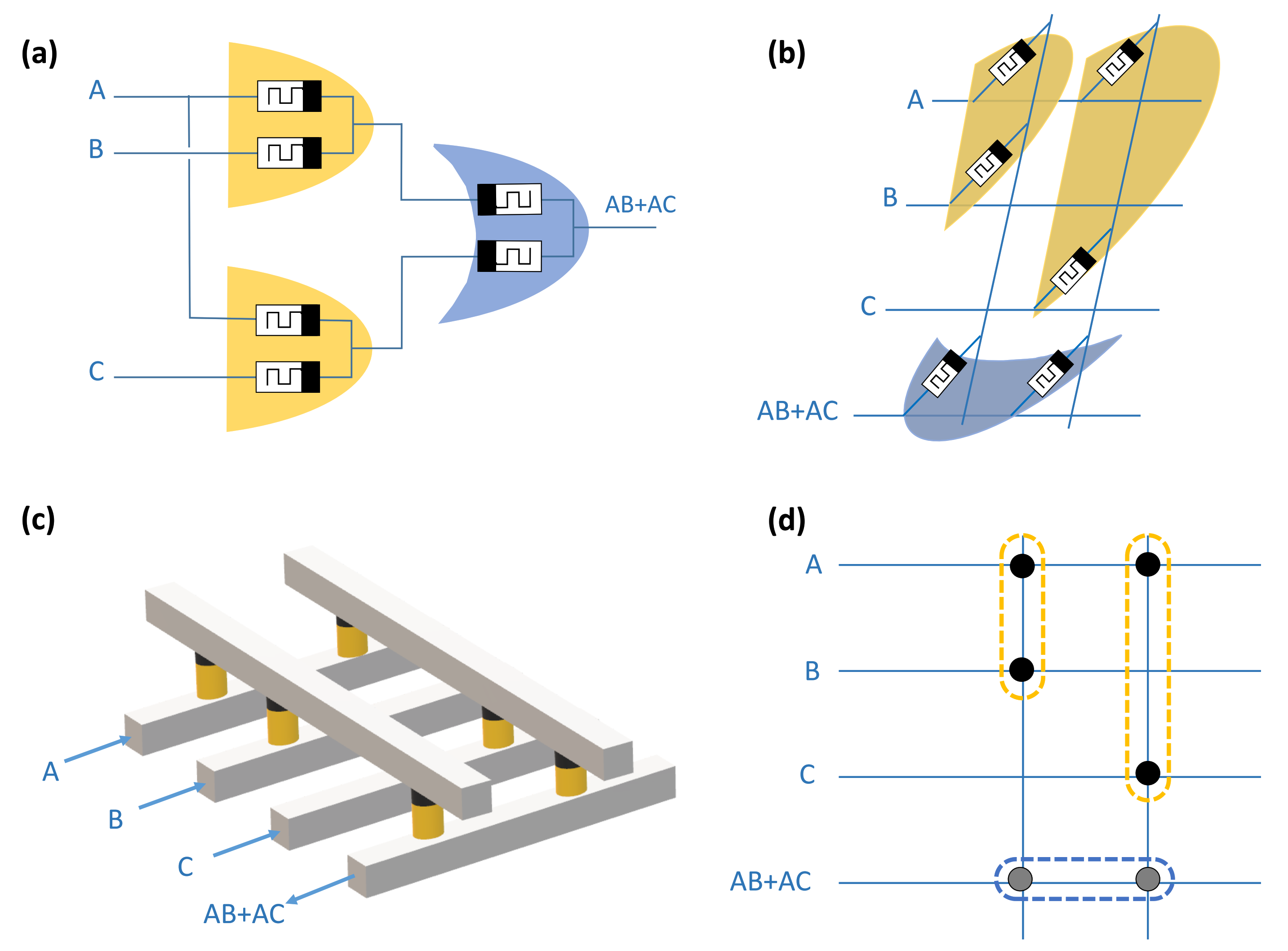
4.1. X-MRL Structure

A memristive crossbar is a two-dimensional grid of memristors distributed along vertical and horizontal nanowires. A memristor is allocated between every vertical nanowire (called a column) and horizontal nanowire (called a row). A memristive crossbar is characterized by its simple and dense structure [26] and could be fabricated on the top of a CMOS layer [27]. The potential applications of memristive crossbars range from memory to logic and from digital circuits to analog circuits. On the other hand, MRL is the only memristor-based logic design style that adopts voltage as a state variable. Thus, our proposed design considers the implementation of a combinational Boolean function in a crossbar topology.
It is well known that any Boolean function could be written in the form of the sum of products (SoP). Accordingly, it can be implemented using MRL-AND and MRL-OR with the aid of CMOS inverters. In order to clarify the proposed method, Figure 7 illustrates the design and implementation of the simple function F = A B + A C . Figure 7a shows that the function F is implemented using two MRL-AND gates and one MRL-OR gate. Figure 7b depicts the schematic layout, which illustrates the equivalent mapping of the function onto a crossbar structure. The vertical pairs of memristors corresponding to MRL-AND generate an output which drives the input of the horizontal pair that represents MRL-OR. Figure 7c presents a 3D view of the resulting crossbar structure. Figure 7d is another simplified representation of the obtained crossbar. The same procedure could be performed to implement other Boolean functions. Although the obtained array is a combination of AND and OR gates, the positive poles of the allocated memristors rely on the same planar side, which is considered to be an advantage at the level of their fabrication.

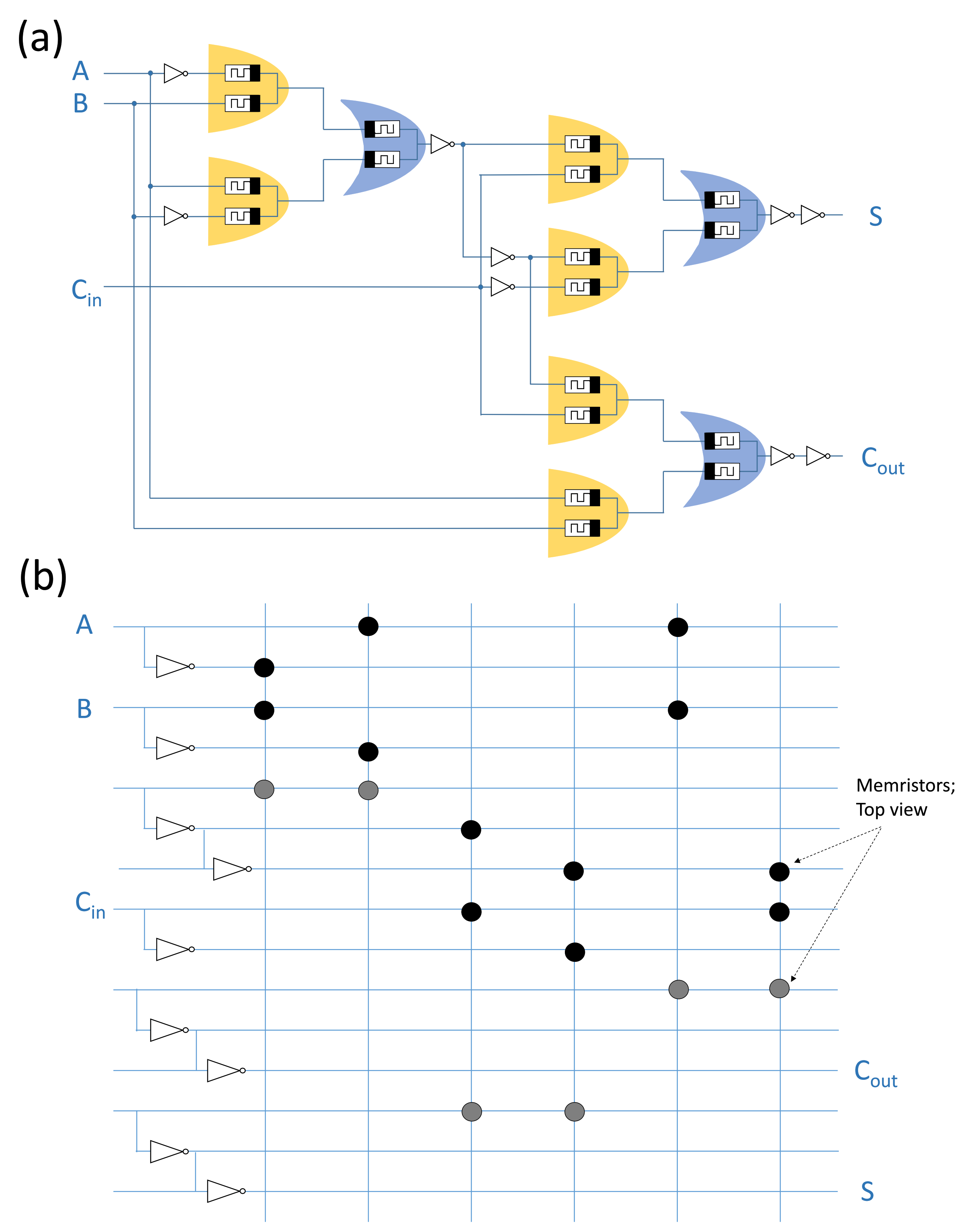
4.2. X-MRL Full Adder
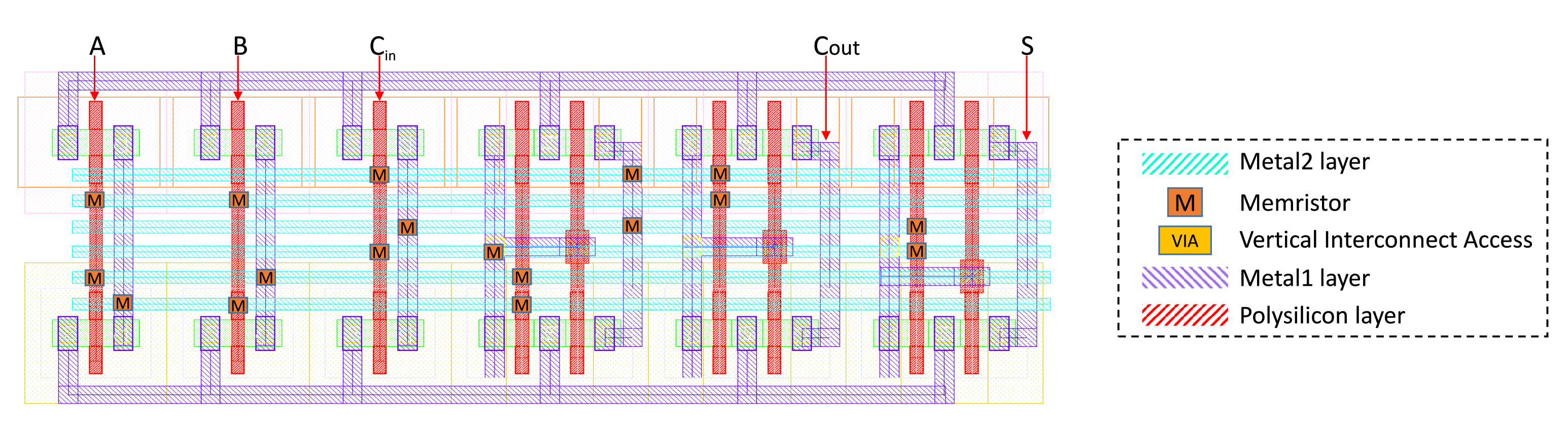
This subsection presents, as an example, the design of the 1 bit full adder using the X-MRL design technique. Equations (10) and (11) present the expressions of the 1-bit full adder in the SoP format.
S = A B C i n = C i n ( A ¯ B + A B ¯ ¯ ) + C i n ¯ ( A ¯ B + A B ¯ )
C o u t = A B + B C i n + A C i n
where A and B are the inputs, C i n is the input carry, S is the 1-bit adder output and C o u t is the output carry. Figure 8a presents the direct form of an MRL based 1-bit full adder. Figure 8b presents the proposed circuit design of the 1-bit full adder using an MRL-based crossbar structure. The design requires 18 memristors, which are distributed among vertical and horizontal wires, in addition to nine CMOS inverters. In the figure, the black vertical pairs of memristors represent the AND gates while the gray horizontal pairs represent the OR gates (as illustrated in Figure 7). The CMOS inverters are responsible for either inverting (NOT operation) and/or performing signal restoration for the logical state of the signal after several cascading stages.
It is worth noting that the designed X-MRL array is different from conventional crossbar arrays as a certain number of crosspoints are vacant. In this array, all memristors are accessed simultaneously, leading to deterministic current paths. Thus, there are no unexpected current paths, and consequently it is sneak-path free.

4.3. Layout

The circuit of the full adder is composed of a memristor crossbar layer in addition to a few inverters. Figure 9 presents the layout of the circuit using the Cadence Virtuoso tool. In this layout, the positions of the allocated memristors are assigned virtually due to the lack of their definition in the Cadence library. The layout is mainly composed of three layers. The first layer is the polysilicon layer, which is dedicated to the connection of the gates of NMOS and PMOS transistors. This layer is presented in red in the figure. The second and third layers, which are called Metal1 and Metal2 and presented in the figure in violet and blue, respectively, are dedicated to the wiring. In order to achieve the desired crossbar structure, horizontal wires are constructed in the Metal2 layer, while for the vertical wires, the connections that are already utilized for the implementation of the required CMOS inverters are reused to complete the crossbar structure. However, the height of the utilized memristors is too short (around 10 nm [28]) to allow the linkage of horizontal and vertical wires through two different layers. Therefore, these links are achieved through vertical interconnect accesses (VIAs) as demonstrated in [29]. Figure 10 is a schematic view and cross-sectional transmission electron microscopy (TEM) image of a memristor integrated with a CMOS in the same die [29].
The allocated memristors in our proposed layout are implemented at the top of the VIAs immediately under the Metal2 layer. Accordingly, the CMOS inverters occupy most of the utilized area, and the additional Metal2 layer is reserved for memristors. In fact, the designed crossbar causes N-wells and P-wells to be slightly too far from each other. The obtained layout design could be made more compact if the memristors were implemented immediately above the CMOS devices. However, this prevents the realization of an X-MRL approach, as more routing signals would be then added, leading to more wiring in Metal1 and Metal2 layers. This would again cause N-wells and P-wells to be distant from each other, increasing the area overhead.

5. Simulation and Performance Analysis

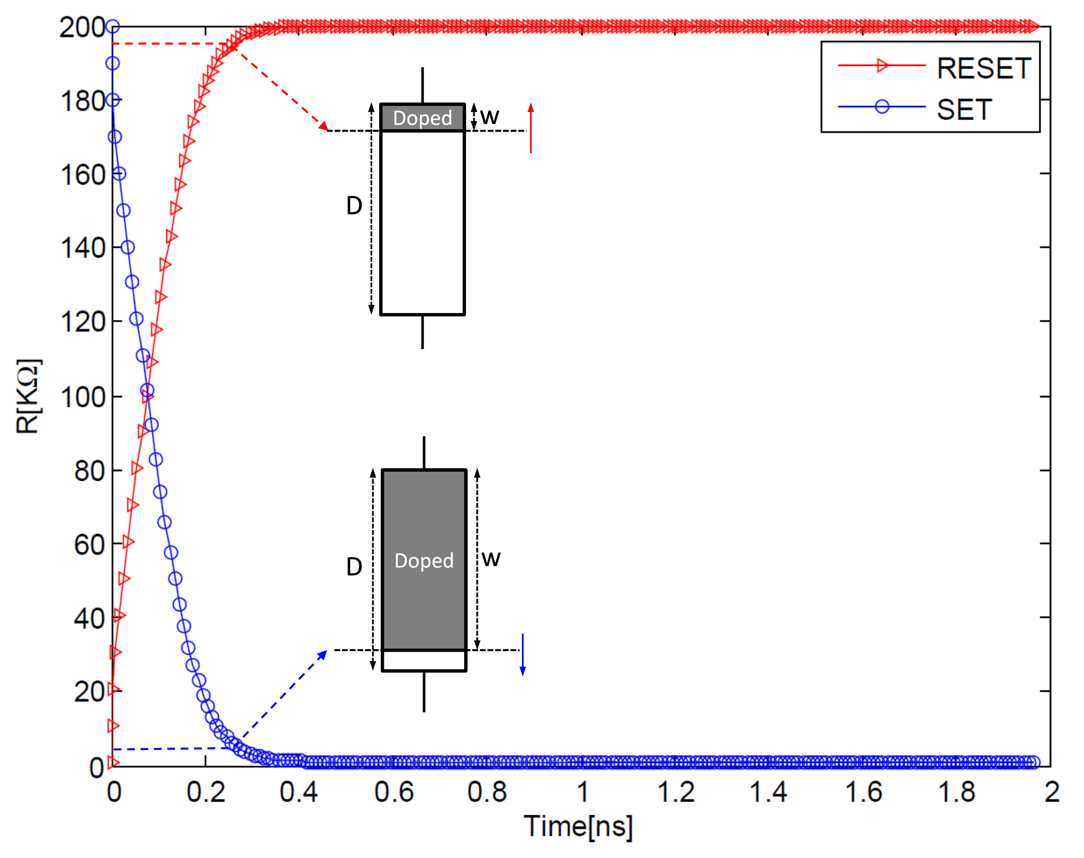
5.1. Memristor Model Fitting

Physical models of memristors, which are based on filament formation and rupture [30,31] rather than a simplified moving boundary (as described by HP), are more realistic. However, compared to physical models, a compact model (e.g., VTEAM) provides the possibility of rapidly reproducing the phenomenological electrical behavior of memristors with a low computational cost. Accordingly, the VTEAM model has been adopted in this paper for simulation. The VTEAM model can mathematically fit the measured electrical behaviors of a memristor and can be easily extended to different types of memristors. In contrast, other models (e.g., the Stanford model [32]) focus on a specific type of memristors or even a single memristor device. Table 1 provides the experimental data of various available memristors with their respective properties. Other memristive devices that belong to the STT-MTJ family [33,34] are excluded from the table. This is due to the fact that MTJ devices usually exhibit a low R O F F / R O N ratio that does not suit the operation of MRL. Of the memristors listed in Table 1, the HfO x memristor which has been reported in [35] has properties which suit the MRL gates. The device is characterized by a low switching delay 300 ps at a low operating voltage of 1.4 V.
These characteristics mean that this memristor is eligible to be implemented in the same die with the current CMOS devices. Important work regarding the implementation of the VTEAM model parameters that fit with the physical parameters of HfO x is described in [35]. Table 2 shows the determined VTEAM model parameters. The model parameters are chosen to produce a switching delay of 300 ps for a voltage pulse of 1.4 V, as reported in [35].
Figure 11 shows the switching behavior of the memristor corresponding to SET and RESET pulses. The device is assumed to be completely switched when the boundary position w reaches either 1% or 99% of the total length D of the memristor, corresponding to SET ( V s e t = 1.4 V) and RESET ( V r e s e t = 1.4 V) operations, respectively. The boundary conditions of the memristor are managed by a Biolek window function. The mathematical function of the Biolek window [41], which is described in Equation (12), provides a continuous and smooth transition of the boundary when reaching one of the extremities of the memristor.
f ( x ) = 1 ( x s t p ( i ( t ) ) ) 2 p
where s t p ( . ) represents a unit step function and p is a positive integer. Low values of p lead to a smooth transition of the boundary of the memristor when reaching its extremities, whereas high values lead to sharp transitions.

5.2. Performance Analysis

A transient simulation was conducted for the proposed design of the X-MRL-based full adder in the Cadence Virtuoso environment. CMOS 65 nm technology at the standard 1.2 V was adopted. Figure 12 shows all the possible combinations at the inputs A, B and C i n in addition to the corresponding outputs S and C o u t . The performance is analyzed below for the proposed design.

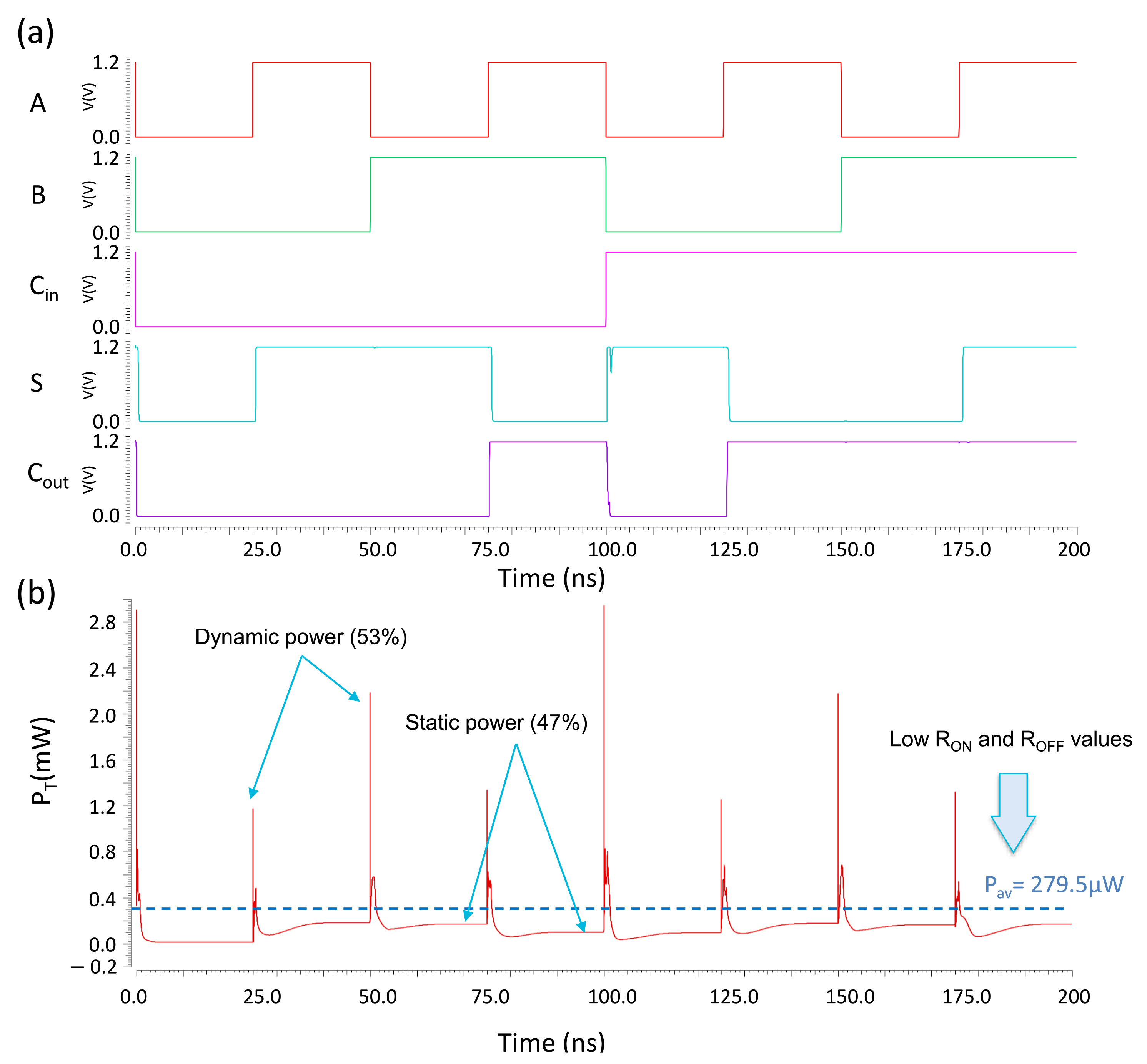
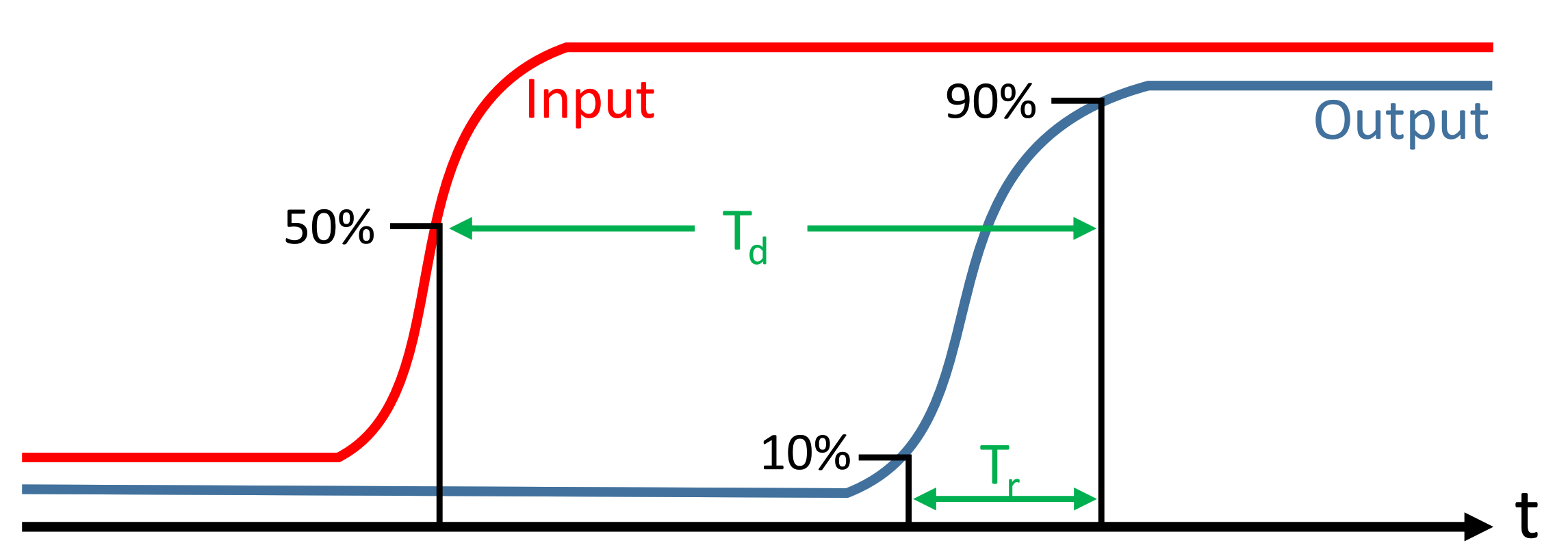
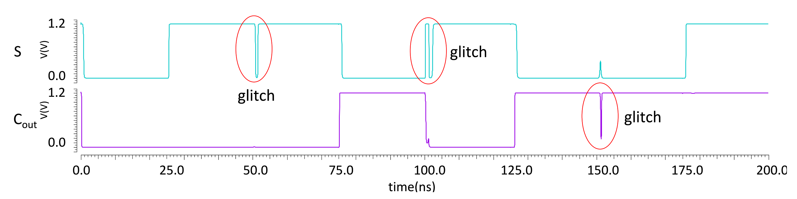
5.2.1. Timing Analysis

Figure 13 presents the definition of the rising time ( T r ) and the time delay ( T d ). Accordingly, the conducted simulation of the proposed design shows that these extracted parameters ( T r and T d ) change among different value combinations of A, B and C i n . The maximum recorded values are as follows: T r = 82 ps, T d = 1.2 ns, and T f = 586 ps, where T f is the falling time. These values are considered for the worst-case performance. The conducted simulation shows that the values T r , T f and T d are affected by the switching speed of the memristor, which in turn can be controlled by K o n and K o f f . On the other hand, slowing down the switching speed of the memristors increases the glitches. Figure 14 shows the appearance of glitches when reducing K o n and K o f f levels to 0.01 m/s and 0.01 m/s, respectively. Particularly, the high-resistance state ( R O F F ) of the memristors has a direct effect on the value of T d , which decreases when increasing the value of R O F F . Therefore, the total delay is directly affected by the memristor’s physical properties. Moreover, it is observed that increasing R O F F acts as a filter for the glitches. This is due to the fact that a larger R O F F value minimizes the voltage drop at the output ports of MRL gates. Reducing the voltage drop speeds up the switching of the next cascaded MRLs, resulting in a smaller number of glitches.

5.2.2. Energy Consumption

Figure 12b shows the total instantaneous power p T ( t ) consumed by the proposed design of the full adder. The peak values in p T ( t ) refer to the dynamic power consumption. The lower bound in p T ( t ) , which is formed after the end of each transition, corresponds to the static power. A slight difference appears between the levels of the static power recorded after each transition. This difference is due to the change in the equivalent resistance state of the cascaded memristors for a new combination of the input signals A, B and C i n , which in turn leads to a different level of current leakage. The average power consumed in the proposed design of the full adder is P a v = 279.5 μ W. This value is of P a v is evaluated at a frequency f of 200 MHz, which is near to the maximum possible frequency at the inputs of the full adder with a hybrid structure.
The value of the average power consumption is relatively high for a full adder circuit. This is due to the low values of R O N and R O F F of the adopted memristor device compared to the source-to-drain dynamic resistance in MOSFETs, which minimizes the leakage in current. Memristive devices are still being actively explored and developed using a variety of materials and deposition techniques. Thus, there is the potential for the device characteristics to be improved. Memristors with high values of R O N and R O F F have to be developed in order to achieve hybrid architectures with low power consumption.

5.2.3. Utilized Area

A single memristor has an area in the order of 4 F 2 [28], where F is the minimum feature size. Thus, memristors are implemented at the top of the CMOS due to their nano-scale and compatibility at the level of fabrication. Thus, the allocated memristors in the proposed X-MRL design do not add any overhead in terms of the implementation area. The total required area refers to that occupied by CMOS devices only, which depends on the number of inverters, as discussed in Section 4.3. Figure 9 presents the proposed layout. The total area of the X-MRL design is 8.16 μ m 2 compared to the area of 14.78 μ m 2 utilized in the case of a pure CMOS implementation, leading to a 44.79% area saving.

6. Comparison

The proposed hybrid memristor–CMOS-based full adder was compared with previous published designs dedicated to the 1-bit full adder. Note that related works in the literature lack an estimation of the utilized area of their proposed designs. Moreover, in order to achieve a fair comparison in terms of energy consumption, the energy was evaluated for each additional operation. The time period for an addition operation in our proposed full adder design was set to be the minimum possible time (i.e., the maximum frequency). This subsection presents the comparison summary, which is also shown in Table 3.
In [9], an optimized implementation of an MRL based 1-bit full adder is proposed. The authors developed an algorithm to search for the best form of the Boolean functions of the sum (S) and carry (C). The desired form should lead to an implementation with the minimum possible number of CMOS inverters. The inverter positions are allocated in such a way that removes signal degradation. The proposed circuit design of the full adder in [9] has a smaller number of memristors as well as CMOS transistors, with reductions of 11.1 % and 33.3 % , respectively, compared to our proposed design. However, the obtained logic function in [9] is not in the form of SoP. Thus, it is not possible to allocate memristors in a crossbar structure. This leads to more wiring at the fabrication stage, which in turn increases the implementation area dramatically. As regards energy consumption, the values reported in [9] are in the normalized form; thus, they cannot be used for comparison.
In [42], the authors presented a hybrid memristor–CMOS-based full adder circuit based on MRL. The adder is comprised of 18 memristors and 8 MOSFETs, which corresponds to a 66.6 % reduction in the number of MOSFETs compared to our proposed design. However, the energy and the step delay in [42] are much higher compared to our presented X-MRL design. The layout is not considered by the authors.
In [43], a design for a 1 bit full adder was proposed based on memristor MAGIC-NOR and NOT gates. A crossbar structure was adopted and several optimization techniques were used to minimize the number of rows and columns of the crossbar as well as the number of computational steps. It has been shown that a compromise exists between the size of the crossbar and the necessary number of steps to perform a full addition. A minimum size of 3 × 3 crossbars (i.e., nine memristors) with a total latency of 35 computational steps is achieved. In contrast, our proposed design uses 18 memristors distributed in a crossbar structure in addition to nine CMOS inverters. The output is evaluated in one computational step. Concerning energy consumption, the proposed design in [43] consumes 0.3 pJ to achieve a 1 bit full addition process, whereas our proposed design consumes 0.69 pJ.
In [23], an N-bit addition was performed using MAGIC operations (i.e., NOR and NOT gates). Several approaches were presented by the authors for realizing logic within crossbars. The best of these approaches in terms of latency corresponded to 10 N + 3 computational steps, which leads to 13 clock cycle for the case of a 1 bit full adder. However, 13 N 3 memristors are reserved (i.e., 10 memristors for N = 1 ) to accomplish the 1 bit addition process. For the purpose of minimizing the number of reserved memristors inside the crossbar, an area optimized crossbar structure was also proposed in [23]. Only five memristors were utilized; however, 15 N (i.e., 15 for N = 1 ) computational steps were required to achieve 1-bit full addition. As a result, our proposed design, which requires one computational step, outperforms the designs presented in [23] in terms of latency. Regarding the energy consumption, all the proposed approaches in [23] have almost the same energy dissipation, which is about 3.16 pJ for the case of N = 1 . Thus, the proposed design in [23] consumes 4.5 times more energy than our proposed design.
In [44], an N-bit ripple carry adder (RCA) circuit in a memristor crossbar structure was presented. The MAGIC design style was used to implement the logic gates. By considering N = 1 , which is the case of 1 bit addition, the proposed crossbar MAGIC-based design requires 15 memristors and can perform the addition operation in 13 clock cycles. Compared to our proposed design, the adder design in [44] needs 13 times more clock cycles to perform addition operation, while it requires three fewer memristors to be implemented. On the other hand, our design consumes 1.01 times more energy than the proposed design in [44].
In [24], logic operations were realized by two methods using MAGIC. The first method corresponds to a naive mapping: it maps the NOR/NOT netlist into a single row of the crossbar. For the case of 1 bit full addition, 12 NOT/NOR sequential operations were required for a total number of 15 memristors. The overall energy consumption is estimated as 0.68 pJ. The second method corresponds to the compact mapping: in this method, NOR/NOT MAGIC operations are performed on rows and columns of a crossbar to realize logic functions. A 1 bit full addition process is performed on an 8 × 3 crossbar structure (i.e., 24 memristors) and requires 16 computational steps. The overall energy consumption is evaluated as 0.89 pJ. Compared to our design, the naive mapping and the compact mapping consume 1.01 times less and 1.28 times more energy, respectively.
In [45], the authors proposed a 1 bit full adder that was designed using IMPLY logic. The proposed design needs 23 computational steps to perform the addition. The 1 bit full adder proposed in [45] requires six memristors, which is 33.3 % of the memristors utilized in our design. However, the IMPLY logic design approach adopts three different voltage levels ( V C O N D , V S E T and V C L E A R ). Thus, additional circuitry such as analog multiplexers should be added to drive the allocated memristors. This induces an overhead in terms of the total utilized area when compared to our proposed design. Note that the energy consumption was not considered by the authors.
In [46], the authors proposed an IMPLY-based semi-serial adder with a respective addition algorithm. The N-bit full adder is implemented using 2 N + 6 memristors, which correspond to eight memristors for a 1 bit full adder. Compared to our proposed X-MRL design, the authors use 55.5 % fewer memristors. The N-bit addition in [46] is completed within 10 N + 2 steps, which correspond to 12 steps for 1 bit addition. Each step requires 30 μ s to be completed. Thus, our proposed X-MRL full adder design, which requires one computational step ( 2.5 ns in total), outperforms that in [46] in terms of latency.
The authors of [47] presented the design of a semi-parallel adder based on IMPLY. As compared to the semi-serial adder mentioned above, the semi-parallel adder reduces the number of memristors to five, but this comes at the cost of an increased number of computational steps and step delay. The full adder design in [47] uses a smaller number of memristors compared to our proposed design. However, it requires a higher number of steps and larger step delay.
Table 3 summarizes the comparison results presented above. The table illustrates the key advantage of the proposed approach regarding the reduced number of computational steps with respect to other existing designs. The energy consumption remains comparable. The Energy.Delay metric is used for a global direct evaluation. This metric combines both delay and energy consumption. As shown in the table, our proposed design outperforms all existing related ones. The improvement in Energy.Delay is between × 5.7 and × 31 .
On the other hand, for the works that have adopted MAGIC and IMPLY in [23,24,43,44,45], the initialization and the evaluation of the rows and columns of the memristive crossbar require a separate CMOS controller. Moreover, a conversion mechanism is required in these designs. This mechanism includes a sensing amplifier to convert the resulting stored bits from the resistance state to the voltage state [8]. These additional peripheral drivers result in additional overheads in area and power consumption.

7. Conclusions

In this paper, an MRL-based crossbar design—namely, X-MRL—is proposed. The X-MRL approach is dedicated to the implementation of combinational logic. The design methodology of X-MRL efficiently integrates memristors with CMOS devices to improve density and scalability. Using X-MRL, a Boolean function is represented using pairs of memristors mapped efficiently into a crossbar structure. The obtained memristive crossbar is stacked at the top of the CMOS layer. For evaluation purposes, we designed a hybrid memristor–CMOS full adder based on the X-MRL approach. Based on a realistic memristor parameter model and CMOS 65 nm process, the design was simulated in the Cadence Virtuoso environment. The obtained layout of the full adder showed a 44.79% area reduction compared to that implemented with pure CMOS technology. Moreover, the Energy.Delay metric was used for comparison. This revealed a significant improvement (between × 5.7 and × 31 ) with respect to the available literature. As future work, the proposed X-MRL design may be considered for the implementation of flexible logic blocks.

Author Contributions

Conceptualization, K.A.A.; methodology, K.A.A. and A.B.; design, K.A.A.; software, K.A.A.; validation, K.A.A. and A.B.; investigation, A.B., M.R., J.-P.D. and J.J.; writing—original draft preparation, K.A.A.; writing—review and editing, M.R., A.B. and J.-P.D.; supervision, M.R., A.B., J.-P.D. and J.J.; All authors have read and agreed to the published version of the manuscript.

Funding

This research was partially funded by Carnot TSN—IMT Atlantique through the FLEXDEM project.

Conflicts of Interest

The authors declare no conflict of interest.

References

  1. Chua, L. Memristor-The missing circuit element. IEEE Trans. Circuit Theory 1971, 18, 507–519. [Google Scholar] [CrossRef]
  2. Strukov, D.B.; Snider, G.S.; Stewart, D.R.; Williams, R.S. The missing memristor found. Nature 2008, 453, 80–83. [Google Scholar] [CrossRef] [PubMed]
  3. Mladenov, V. Analysis of memory matrices with HfO2 memristors in a PSpice environment. Electronics 2019, 8, 383. [Google Scholar] [CrossRef] [Green Version]
  4. Hamdioui, S.; Du Nguyen, H.A.; Taouil, M.; Sebastian, A.; Le Gallo, M.; Pande, S.; Schaafsma, S.; Catthoor, F.; Das, S.; Redondo, F.G.; et al. Applications of computation-in-memory architectures based on memristive devices. In Proceedings of the Design, Automation & Test in Europe Conference & Exhibition (DATE), Florence, Italy, 25–29 March 2019; pp. 486–491. [Google Scholar]
  5. Kvatinsky, S.; Belousov, D.; Liman, S.; Satat, G.; Wald, N.; Friedman, E.G.; Kolodny, A.; Weiser, U.C. MAGIC—Memristor-aided logic. IEEE Trans. Circuits Syst. II Express Briefs 2014, 61, 895–899. [Google Scholar] [CrossRef]
  6. Kvatinsky, S.; Satat, G.; Wald, N.; Friedman, E.G.; Kolodny, A.; Weiser, U.C. Memristor-based material implication (IMPLY) logic: Design principles and methodologies. IEEE Trans. VLSI Syst. 2014, 22, 2054–2066. [Google Scholar] [CrossRef]
  7. Reuben, J.; Ben-Hur, R.; Wald, N.; Talati, N.; Ali, A.H.; Gaillardon, P.E.; Kvatinsky, S. Memristive logic: A framework for evaluation and comparison. In Proceedings of the 27th International Symposium on Power and Timing Modeling, Optimization and Simulation (PATMOS), Thessaloniki, Greece, 25–27 September 2017. [Google Scholar]
  8. Kvatinsky, S.; Wald, N.; Satat, G.; Kolodny, A.; Weiser, U.C.; Friedman, E.G. MRL—Memristor ratioed logic. In Proceedings of the International Workshop on Cellular Nanoscale Networks and their Applications, Turin, Italy, 29–31 August 2012. [Google Scholar]
  9. Liu, B.; Wang, Y.; You, Z.; Han, Y.; Li, X. A signal degradation reduction method for memristor ratioed logic (MRL) gates. IEICE Electron. Express 2015, 12, 20150062. [Google Scholar] [CrossRef] [Green Version]
  10. Chowdhury, J.; Das, K.; Rout, K. Implementation Of 24T Memristor Based Adder Architecture With Improved Performance. Int. J. Electr. Electron. Data Commun. 2015, 3, 91–94. [Google Scholar]
  11. Cho, K.; Lee, S.J.; Eshraghian, K. Memristor-CMOS logic and digital computational components. Microelectron. J. 2015, 46, 214–220. [Google Scholar] [CrossRef]
  12. Ali, K.A.; Rizk, M.; Baghdadi, A.; Diguet, J.P.; Jomaah, J. MRL Crossbar-Based Full Adder Design. In Proceedings of the 26th IEEE International Conference on Electronics, Circuits and Systems (ICECS), Genoa, Italy, 27–29 November 2019; pp. 674–677. [Google Scholar]
  13. Pickett, M.D.; Strukov, D.B.; Borghetti, J.L.; Yang, J.J.; Snider, G.S.; Stewart, D.R.; Williams, R.S. Switching dynamics in titanium dioxide memristive devices. J. Appl. Phys. 2009, 106, 074508. [Google Scholar] [CrossRef]
  14. Yang, J.J.; Pickett, M.D.; Li, X.; Ohlberg, D.A.; Stewart, D.R.; Williams, R.S. Memristive switching mechanism for metal/oxide/metal nanodevices. Nat. Nanotechnol. 2008, 3, 429–433. [Google Scholar] [CrossRef]
  15. Lehtonen, E.; Laiho, M. CNN using memristors for neighborhood connections. In Proceedings of the International Workshop on Cellular Nanoscale Networks and their Applications (CNNA), Berkeley, CA, USA, 3–5 February 2010. [Google Scholar]
  16. Simmons, J.G. Generalized Formula for the Electric Tunnel Effect between Similar Electrodes Separated by a Thin Insulating Film. J. Appl. Phys. 1963, 34. [Google Scholar] [CrossRef] [Green Version]
  17. Kvatinsky, S.; Friedman, E.G.; Kolodny, A.; Weiser, U.C. TEAM: Threshold adaptive memristor model. IEEE Trans. Circuits Syst. I Regul. Pap. 2013, 60, 211–221. [Google Scholar] [CrossRef]
  18. Kvatinsky, S.; Ramadan, M.; Friedman, E.G.; Kolodny, A. VTEAM: A general model for voltage-controlled memristors. IEEE Trans. Circuits Syst. II Express Briefs 2015, 62, 786–790. [Google Scholar] [CrossRef]
  19. Kvatinsky, S.; Kolodny, A.; Weiser, U.C.; Friedman, E.G. Memristor-based IMPLY logic design procedure. In Proceedings of the IEEE International Conference on Computer Design (ICCD), Amherst, MA, USA, 9–12 October 2011. [Google Scholar]
  20. Bickerstaff, K.; Swartzlander, E.E. Memristor-based arithmetic. In Proceedings of the Conference Record of the Asilomar Conference on Signals, Systems and Computers, Pacific Grove, CA, USA, 7–10 November 2010. [Google Scholar]
  21. Rahman, K.C.; Hammerstrom, D.; Li, Y.; Castagnaro, H.; Perkowski, M.A. Methodology and design of a massively parallel memristive stateful IMPLY logic-based reconfigurable architecture. IEEE Trans. Nanotechnol. 2016, 15, 675–686. [Google Scholar] [CrossRef]
  22. Hur, R.B.; Kvatinsky, S. Memristive memory processing unit (MPU) controller for in-memory processing. In Proceedings of the IEEE International Conference on the Science of Electrical Engineering (ICSEE), Eilat, Israel, 16–18 November 2016. [Google Scholar]
  23. Talati, N.; Gupta, S.; Mane, P.; Kvatinsky, S. Logic design within memristive memories using memristor-aided loGIC (MAGIC). IEEE Trans. Nanotechnol. 2016, 15, 635–650. [Google Scholar] [CrossRef]
  24. Gharpinde, R.; Thangkhiew, P.L.; Datta, K.; Sengupta, I. A Scalable In-Memory Logic Synthesis Approach Using Memristor Crossbar. IEEE Trans. VLSI Syst. 2018, 26, 355–366. [Google Scholar] [CrossRef]
  25. Teimoori, M.; Ahmadi, A.; Alirezaee, S.; Ahmadi, M. A novel hybrid CMOS-memristor logic circuit using Memristor Ratioed Logic. In Proceedings of the IEEE Canadian Conference on Electrical and Computer Engineering (CCECE), Vancouver, BC, Canada, 15–18 May 2016. [Google Scholar]
  26. Williams, R.S. Finding the missing memristor. Keynote Talk at UC San Diego CNS Winter, California, 2010. [Google Scholar]
  27. Xia, Q.; Robinett, W.; Cumbie, M.W.; Banerjee, N.; Cardinali, T.J.; Yang, J.J.; Wu, W.; Li, X.; Tong, W.M.; Strukov, D.B.; et al. Memristor- CMOS hybrid integrated circuits for reconfigurable logic. Nano Lett. 2009, 9, 3640–3645. [Google Scholar] [CrossRef]
  28. Yang, J.J.; Strukov, D.B.; Stewart, D.R. Memristive devices for computing. Nat. Nanotechnol. 2013, 8, 13–24. [Google Scholar] [CrossRef]
  29. Tsunoda, K.; Kinoshita, K.; Noshiro, H.; Yamazaki, Y.; Iizuka, T.; Ito, Y.; Takahashi, A.; Okano, A.; Sato, Y.; Fukano, T.; et al. Low power and high speed switching of Ti-doped NiO ReRAM under the unipolar voltage source of less than 3V. In Proceedings of the IEEE International Electron Devices Meeting (IEDM), Washington, DC, USA, 10–12 December 2007. [Google Scholar]
  30. Kwon, D.H.; Kim, K.M.; Jang, J.H.; Jeon, J.M.; Lee, M.H.; Kim, G.H.; Li, X.S.; Park, G.S.; Lee, B.; Han, S.; et al. Atomic structure of conducting nanofilaments in TiO 2 resistive switching memory. Nat. Nanotechnol. 2010, 5, 148–153. [Google Scholar] [CrossRef]
  31. Wang, Z.; Joshi, S.; Savel’ev, S.E.; Jiang, H.; Midya, R.; Lin, P.; Hu, M.; Ge, N.; Strachan, J.P.; Li, Z.; et al. Memristors with diffusive dynamics as synaptic emulators for neuromorphic computing. Nat. Mater. 2017, 16, 101–108. [Google Scholar] [CrossRef] [Green Version]
  32. Guan, X.; Yu, S.; Wong, H.S.P. A SPICE compact model of metal oxide resistive switching memory with variations. IEEE Electron Device Lett. 2012, 33, 1405–1407. [Google Scholar] [CrossRef]
  33. Wang, Y.; Zhang, Y.; Deng, E.; Klein, J.O.; Naviner, L.A.; Zhao, W. Compact model of magnetic tunnel junction with stochastic spin transfer torque switching for reliability analyses. Microelectron. Reliab. 2014, 54, 1774–1778. [Google Scholar] [CrossRef]
  34. Wang, Y.; Cai, H.; Naviner, L.A.; Zhang, Y.; Klein, J.O. Compact thermal modeling of spin transfer torque magnetic tunnel junction. Microelectron. Reliab. 2015, 55, 1649–1653. [Google Scholar] [CrossRef]
  35. Lee, H.; Chen, Y.; Chen, P.; Gu, P.; Hsu, Y.; Wang, S.; Liu, W.; Tsai, C.; Sheu, S.; Chiang, P.; et al. Evidence and solution of over-RESET problem for HfOx based resistive memory with Sub-ns switching speed and high endurance. In Proceedings of the IEEE International Electron Devices Meeting, San Francisco, CA, USA, 2 March 2010. [Google Scholar]
  36. Chanthbouala, A.; Garcia, V.; Cherifi, R.O.; Bouzehouane, K.; Fusil, S.; Moya, X.; Xavier, S.; Yamada, H.; Deranlot, C.; Mathur, N.D.; et al. A ferroelectric memristor. Nat. Mater. 2012, 11, 860–864. [Google Scholar] [CrossRef]
  37. Kang, J.; Huang, P.; Gao, B.; Li, H.; Chen, Z.; Zhao, Y.; Liu, C.; Liu, L.; Liu, X. Design and application of oxide-based resistive switching devices for novel computing architectures. IEEE J. Electron Devices Soc. 2016, 4, 307–313. [Google Scholar] [CrossRef]
  38. Baek, I.; Lee, M.; Seo, S.; Lee, M.; Seo, D.; Suh, D.S.; Park, J.; Park, S.; Kim, H.; Yoo, I.; et al. Highly scalable nonvolatile resistive memory using simple binary oxide driven by asymmetric unipolar voltage pulses. In Proceedings of the IEEE International Electron Devices Meeting (IEDM), San Francisco, CA, USA, 13–15 December 2004. [Google Scholar]
  39. Diokh, T.; Le-Roux, E.; Jeannot, S.; Gros-Jean, M.; Candelier, P.; Nodin, J.; Jousseaume, V.; Perniola, L.; Grampeix, H.; Cabout, T.; et al. Investigation of the impact of the oxide thickness and RESET conditions on disturb in HfO2-RRAM integrated in a 65 nm CMOS technology. In Proceedings of the IEEE International Reliability Physics Symposium (IRPS), Monterey, CA, USA, 14–18 April 2013. [Google Scholar]
  40. Lee, H.; Chen, P.; Wu, T.; Chen, Y.; Wang, C.; Tzeng, P.; Lin, C.; Chen, F.; Lien, C.; Tsai, M.J. Low power and high speed bipolar switching with a thin reactive Ti buffer layer in robust HfO2 based RRAM. In Proceedings of the IEEE International Electron Devices Meeting (IEDM), San Francisco, CA, USA, 15–17 December 2008. [Google Scholar]
  41. Biolek, Z.; Biolek, D.; Biolkova, V. SPICE Model of Memristor with Nonlinear Dopant Drift. Radioengineering 2009, 18, 210–214. [Google Scholar]
  42. Mandal, S.; Sinha, J.; Chakraborty, A. Design of Memristor—CMOS based logic gates and logic circuits. In Proceedings of the 2nd International Conference on Innovations in Electronics, Signal Processing and Communication (IESC), Shillong, India, 1–2 March 2019; pp. 215–220. [Google Scholar]
  43. Thangkhiew, P.L.; Gharpinde, R.; Chowdhary, P.V.; Datta, K.; Sengupta, I. Area efficient implementation of ripple carry adder using memristor crossbar arrays. In Proceedings of the International Design & Test Symposium (IDT), Hammamet, Tunisia, 18–20 December 2016. [Google Scholar]
  44. Thangkhiew, P.; Gharpinde, R.; Yadav, D.N.; Datta, K.; Sengupta, I. Efficient implementation of adder circuits in memristive crossbar array. In Proceedings of the IEEE Region 10 Conference (TENCON), Penang, Malaysia, 5–8 November 2017. [Google Scholar]
  45. Teimoory, M.; Amirsoleimani, A.; Shamsi, J.; Ahmadi, A.; Alirezaee, S.; Ahmadi, M. Optimized implementation of memristor-based full adder by material implication logic. In Proceedings of the IEEE International Conference on Electronics, Circuits and Systems (ICECS), Marseille, France, 7–10 December 2014. [Google Scholar]
  46. TaheriNejad, N.; Delaroche, T.; Radakovits, D.; Mirabbasi, S. A semi-serial topology for compact and fast IMPLY-based memristive full adders. In Proceedings of the 17th IEEE International New Circuits and Systems Conference (NEWCAS), Munich, Germany, 23–26 June 2019; pp. 1–4. [Google Scholar]
  47. Rohani, S.G.; Taherinejad, N.; Radakovits, D. A Semiparallel Full-Adder in IMPLY Logic. IEEE Trans. Very Large Scale Integr. Syst. 2019, 28, 297–301. [Google Scholar] [CrossRef]
Figure 1. Memristor: (a) Pinched hysteresis loop, (b) structure: metallic electrodes sandwiching a thin dielectric insulating layer, (c) symbol.
Electronics 10 01018 g001
Figure 2. TiO 2 memristor model according to [2].
Electronics 10 01018 g002
Figure 3. IMPLY gate: (a) schematic of a memristor-based IMPLY gate, (b) truth table of the IMPLY function.
Electronics 10 01018 g003
Figure 4. Structure of MAGIC NOR gate.
Electronics 10 01018 g004
Figure 5. Schematic layout of MRL AND, NAND, OR and NOR gates.
Electronics 10 01018 g005
Figure 6. Logical operations performed with MRL AND gate.
Electronics 10 01018 g006
Figure 7. Example of an MRL logic function performed using X-MRL. Reproduced with permission from [12], Copyright 2019, IEEE.
Electronics 10 01018 g007
Figure 8. One-Bit Full Adder based on the proposed X-MRL structure. Reproduced with permission from [12], Copyright 2019, IEEE.
Electronics 10 01018 g008
Figure 9. Proposed layout for the hybrid memristor–CMOS 1-bit full adder based on the X-MRL design technique.
Electronics 10 01018 g009
Figure 10. Memristor layer at the top of VIAs [29]: (a) a TEM image; (b) a schematic view. Reproduced with permission from [29], Copyright 2019, IEEE.
Electronics 10 01018 g010
Figure 11. Memristor switching time for V s e t = 1.4 V and V r e s e t = 1.4 V according to the device in [35].
Electronics 10 01018 g011
Figure 12. Transient response of the proposed full adder for the input signals A, B and C i n .
Electronics 10 01018 g012
Figure 13. Definition of the rise time T r and delay T d .
Electronics 10 01018 g013
Figure 14. Appearance of glitches when slowing down the switching speed of the memristor. The parameters in Table 2 are adopted except for K o n = 0.01 m/s and K o f f = 0.01 m/s.
Electronics 10 01018 g014
Table 1. Practical memristor devices.
Material R ON (ohm) R OFF (ohm) R OFF / R ON Switching SpeedVoltage RangeReference
TiO 2 - x -->3001 ns−1.5 V to +1.5 V[28]
FTJ 1.6 × 10 5 4.6 × 10 7 >20010 ns−5.6 V to +4.2 V[36]
HfO 2 1.2 × 10 2 10 5 10 3 <1 ns<1.5 V[37]
HfO x <10 k>100 k>100300 ps<1.4 V[35]
TMO-100 k-10 ns to 100 ns3 V[38]
HfO 2 2 × 10 3 2 × 10 5 100-−1.5 V to +1 V[39]
TiN/ TiO x / HfO x /TiN1 k>1 M>10005 ns−1.5 V to +1.5 V[40]
Table 2. VTEAM fitting parameters for the device in [35].
ParameterValueParameterValue
R O N 1 k Ω p2
R O F F 200 k Ω α o n 3
D 3 nm α o f f 3
K o n 0.0162 m/s V o n 0.16 V
K o f f 0.0162 m/s V o f f 0.16 V
x o n 0 nm x o f f 3 nm
Table 3. Comparison with previous approaches.
ReferenceMemristorsCMOS TransistorsEnergyStepsStep DelayEnergy.Delay
(This work)1818 0.69 pJ1 2.5 ns 1.72 pJ.ns
MRL [9]1612-1--
MRL [42]188 93.7 pJ1 44.4 ns 4161 pJ.ns
MAGIC [43]9Peripheral drivers 0.3 pJ35 1.89 ns 19.84 pJ.ns
MAGIC (Optimized no. of steps) [23]10Peripheral drivers 3.16 pJ13 1.3 ns 53.40 pJ.ns
MAGIC (Area optimized) [23]5Peripheral drivers 3.16 pJ15 1.3 ns 61.62 pJ.ns
MAGIC [44]15Peripheral drivers 0.68 pJ13 1.12 ns 9.94 pJ.ns
MAGIC (Naive mapping) [24]15Peripheral drivers 0.68 pJ12 1.43 ns 11.66 pJ.ns
MAGIC (Compact mapping)[24]24Peripheral drivers 0.89 pJ16 1.43 ns 20.36 pJ.ns
IMPLY [45]6Peripheral drivers-23 5 ns-
IMPLY (Semi-serial) [46]8Peripheral drivers-12 30 μ s-
IMPLY (Semi-parallel) [47]5Peripheral drivers-17 50 μ s-
Publisher’s Note: MDPI stays neutral with regard to jurisdictional claims in published maps and institutional affiliations.

