Article

Improving Emission Uniformity of InGaN/GaN-Based Vertical LEDs by Using Reflective ITO/Ag n-Contact

1
LED Division, LG Innotek Co., Paju, Gyeonggi 10842, Korea
2
Department of Materials Science and Engineering, Korea University, Seoul 02841, Korea
*
Author to whom correspondence should be addressed.
Electronics 2021, 10(8), 975; https://doi.org/10.3390/electronics10080975
Submission received: 2 April 2021 / Revised: 14 April 2021 / Accepted: 15 April 2021 / Published: 19 April 2021

Abstract

:
We investigated the effect of Ti/Al and ITO/Ag n-type contacts on the emission uniformity and light output of different chip-size vertical-geometry light-emitting diodes (VLEDs) for vehicle headlamp application. The forward voltage of the Ti/Al-based reference VLEDs decreased from 3.38 to 3.20 V at 1500 mA with increasing chip size from (1280 × 1000 µm2) to (1700 × 1700 µm2), whereas that of the ITO/Ag-based samples changed from 3.37 to 3.15 V. Regardless of chip size, the ITO/Ag-based samples revealed higher light output power than the reference samples. For example, the ITO/Ag-based samples (chip size of 1700 × 1700 µm2) exhibited 3.4% higher light output power at 1500 mA than the reference samples. The ITO/Ag samples underwent less degradation in the Wall-plug efficiency (WPE) than the reference sample. For instance, the ITO/Ag-based samples (1700 × 1700 µm2) gave 4.8% higher WPE at 1500 mA than the reference samples. The ITO/Ag-based samples illustrated more uniform emission than the Ti/Al-based sample. Both the reference and ITO/Ag-based samples underwent no degradation when operated at 1500 mA for 1000 h.

1. Introduction

Light-emitting diodes (LEDs) have been widely applied in a variety of fields, such as solid-state lighting, outdoor display, and vehicle lamp, and biomedical treatments [1,2,3,4,5,6,7,8] because of high luminance efficiency, long lifetime, and low power consumption. In particular, it was shown that vertical-geometry LEDs (VLEDs) demonstrate better current spreading characteristic, heat dissipation efficiency and reliability as compared with lateral and flip-chip geometry LEDs [9,10,11,12,13]. For conventional VLEDs, the n-type contact (and pad) is formed on the top surface and so it blocks the extraction of photons emitted from the active region, resulting in a reduction in the light extraction efficiency (LEE) and emission uniformity [9,10,11,12,13]. Thus, to solve such a problem, buried n-metal contacts have been employed. In other words, n-contact is formed underneath the p-electrode through via holes. The buried n-contact was found to improve LEE and current spreading characteristic [13,14,15,16]. For buried n-contacts, Ti-based metal schemes were typically used to form ohmic contacts [17,18,19]. However, Ti-based contacts have poor reflectance across the visible wavelength range and so they block and absorb photons emitted from the active region. Thus, the region beneath and surrounding the n-contact becomes dimmer than the areas away from the contact. This emission non-uniformity can act as a serious technological issue in micro-LED display and vehicle headlamp applications, where absence of dark space between LED pixels is essentially required [20,21]. For instance, Kim et al. [20] investigated the light output performance of 16 × 16 pixelated micro-LEDs for headlights by enhancing the reflectivity and coverage of the p-electrode. The array was fabricated by multi-level metallization using a photosensitive polyimide inter-metal dielectric (IMD) layer. The variation of dark spaces in emission images was examined as a function of the pixel pitch for the controlled micro-LED array at 20 mA. It was shown that the dark space between pixels almost disappeared at a pixel pitch of 125 μm [20]. Thus, in this study, in order to improve the emission uniformity and light output of LEDs for vertical LED-based vehicle headlamp application, via-hole-type thin film vertical-geometry LEDs with buried reflective ITO/Ag n-contact were fabricated and their electrical and optical properties and reliability were characterized.

2. Materials and Methods

MOCVD was employed to grow vertical-geometry blue (445 nm) InGaN-based LED structures on 6 inch (0001) sapphire substrate. The device epilayer structure is composed of a 30 nm-thick GaN nucleation layer, a 1.5 μm-thick undoped GaN layer, a 5 μm-thick Si-doped n-GaN layer, four pairs of InGaN/GaN multi-quantum wells, a 50 nm-thick Mg-doped AlGaN layer, a 70 nm-thick Mg-doped p-GaN layer. For LED fabrication, the wafers were dipped in a H2SO4: H2O2 (2: 1) solution for 10 min and then rinsed with deionized (DI) water, after which they were cleaned again with acetone, methanol, and DI water in an ultrasonic bath, and blown dry with N2 gas. Then, mesa structure with via hole was defined by ICP-RIE to expose n-GaN. Plasma-enhanced chemical vapor deposition was used to deposit 700 nm-thick SiO2 for passivation (Supplementary Figure S1). As illustrated in Supplementary Figure S1a, for conventional samples, ITO (3 nm) as a p-contact and Ti/Al (10 nm/300 nm) as an n-contact were deposited, where the former was annealed at 650 °C for 40 s in N2 gas, while latter was annealed at 550 °C for 3 min in N2 gas. Finally, Ag/Ni p-reflector (200 nm/50 nm) was deposited. On the other hand, for ITO/Ag (3 nm/200 nm) contact samples, after the deposition of a 700 nm-thick SiO2 passivation layer, n- and p contact regions were exposed by etching. After that, an ITO layer (3 nm) was sputter-deposited and annealed at 650 °C for 40 s, followed by the e-beam deposition of Ag/Ni (200 nm/50 nm), that serve as n- and p-type contacts. It should be stressed that the use of ITO/Ag contact reduces the fabrication process of conventional samples by two steps (Supplementary Figure S1b). Next, Ni-Sn wafer bonding metal alloy was e-beam deposited and bonded to a 6-inch metal support at 300 °C, after which the laser lift-off (LLO) process using KrF excimer laser was performed to separate LED structure from the sapphire substrate. The undoped GaN was etched away by ICP-etching to expose n-GaN, whose surface was textured with a heated KOH solution. Schematic diagrams of vertical-geometry LEDs are illustrated in Supplementary Figure S1a–c and Supplementary Figure S2. It should be stressed that use of ITO/Ag reflector reduce the fabrication process by two steps, resulting in cost reduction, as demonstrated in Supplementary Figure S1a–c. For headlamp application, square-shape active area and bar-like p-electrode were used in order to minimize dark space and to enhance the uniformity (Supplementary Figure S3). To characterize the electrical and optical properties, all LED chips were packaged. The electrical and optical properties of the packaged samples were assessed with integrating sphere (Instrument systems GmbH. ISP 500), spectroscope (CAS 140CT), and source meter (Keithley KE2601A). A line profiler was used to examine the emission uniformity of the samples. It should be noted that for each sample, hundreds of chips were examined and their average electrical and optical characteristics are presented.

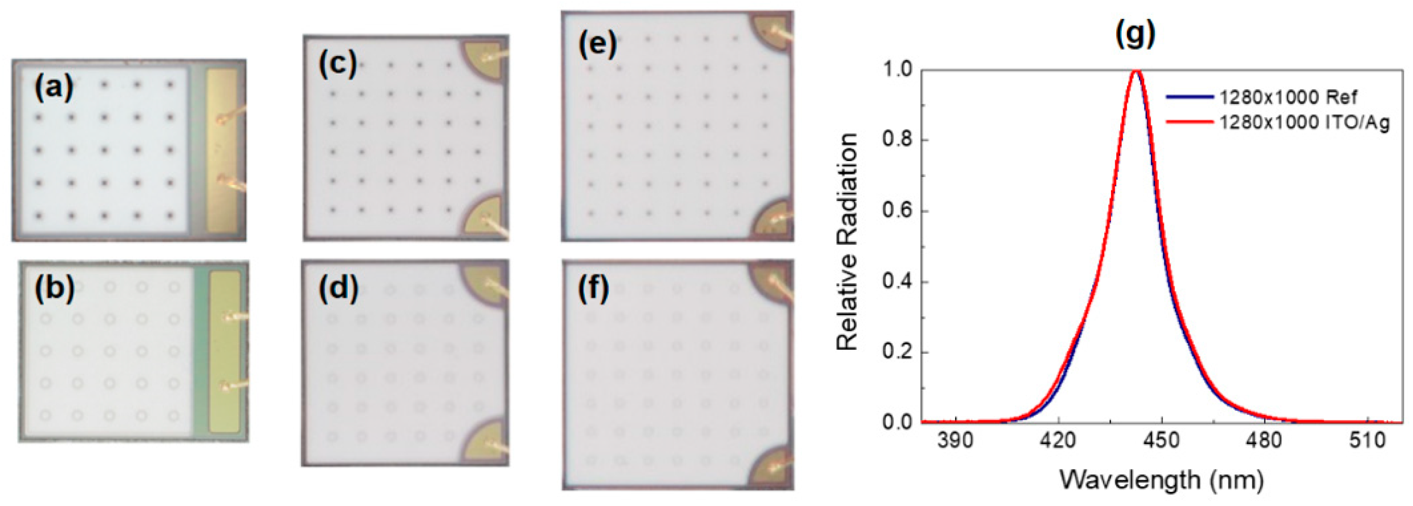
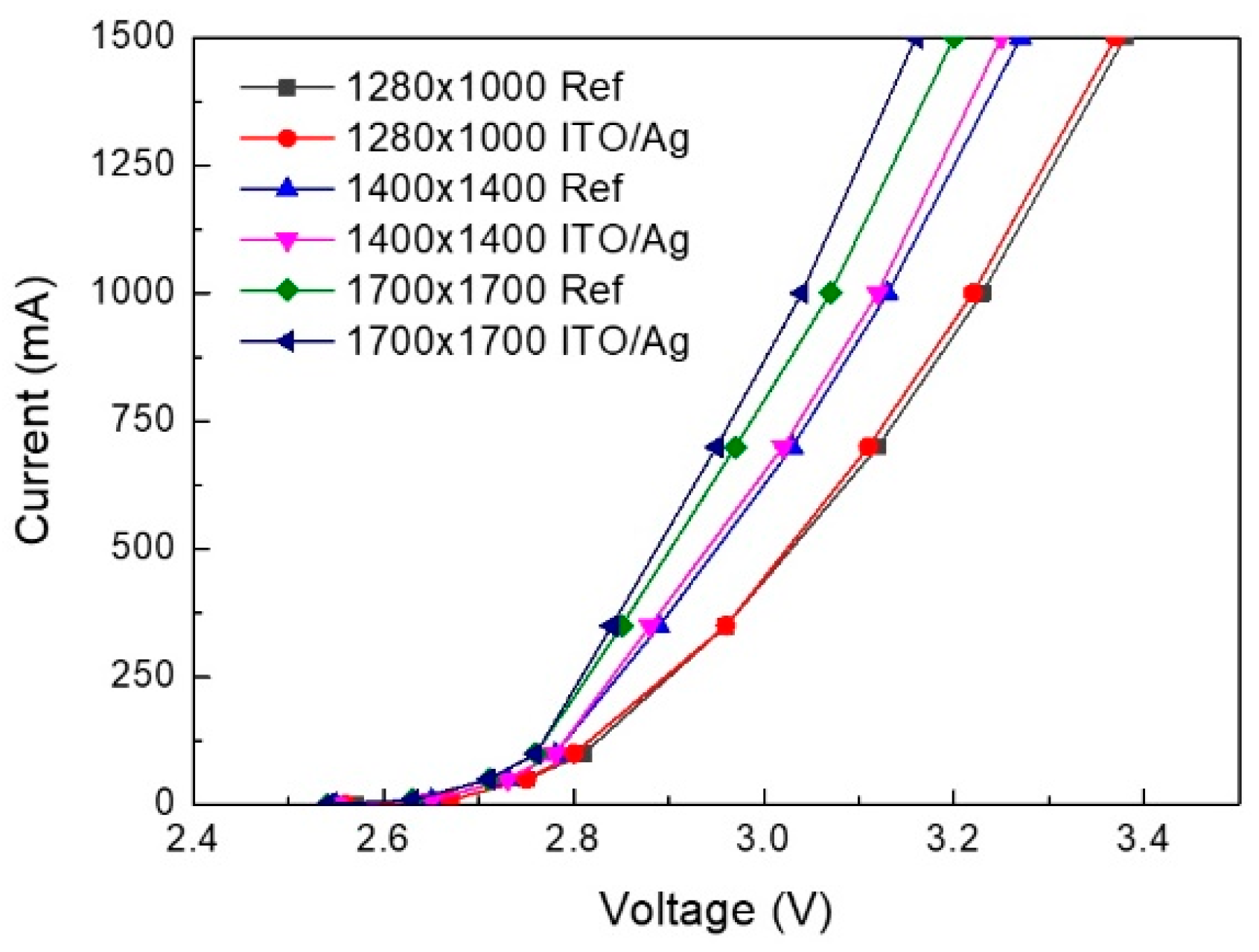
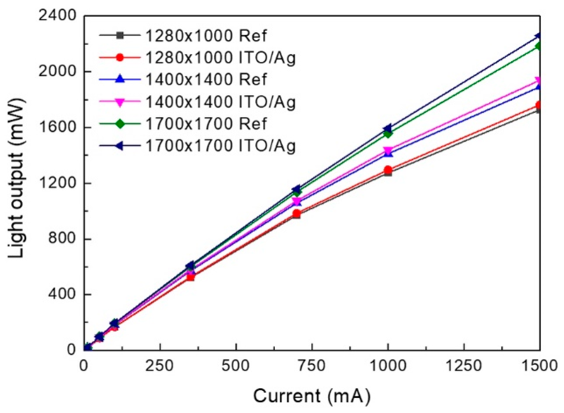
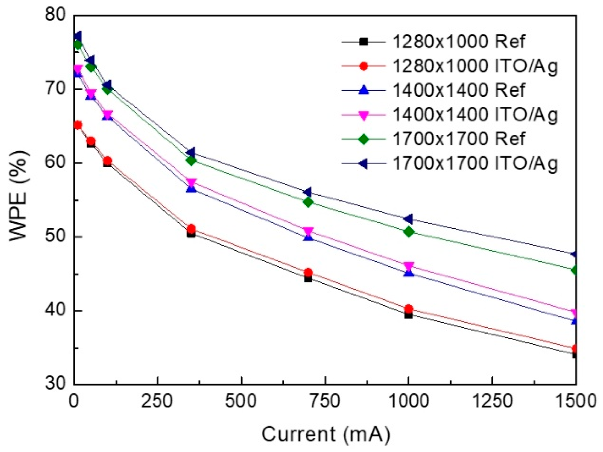
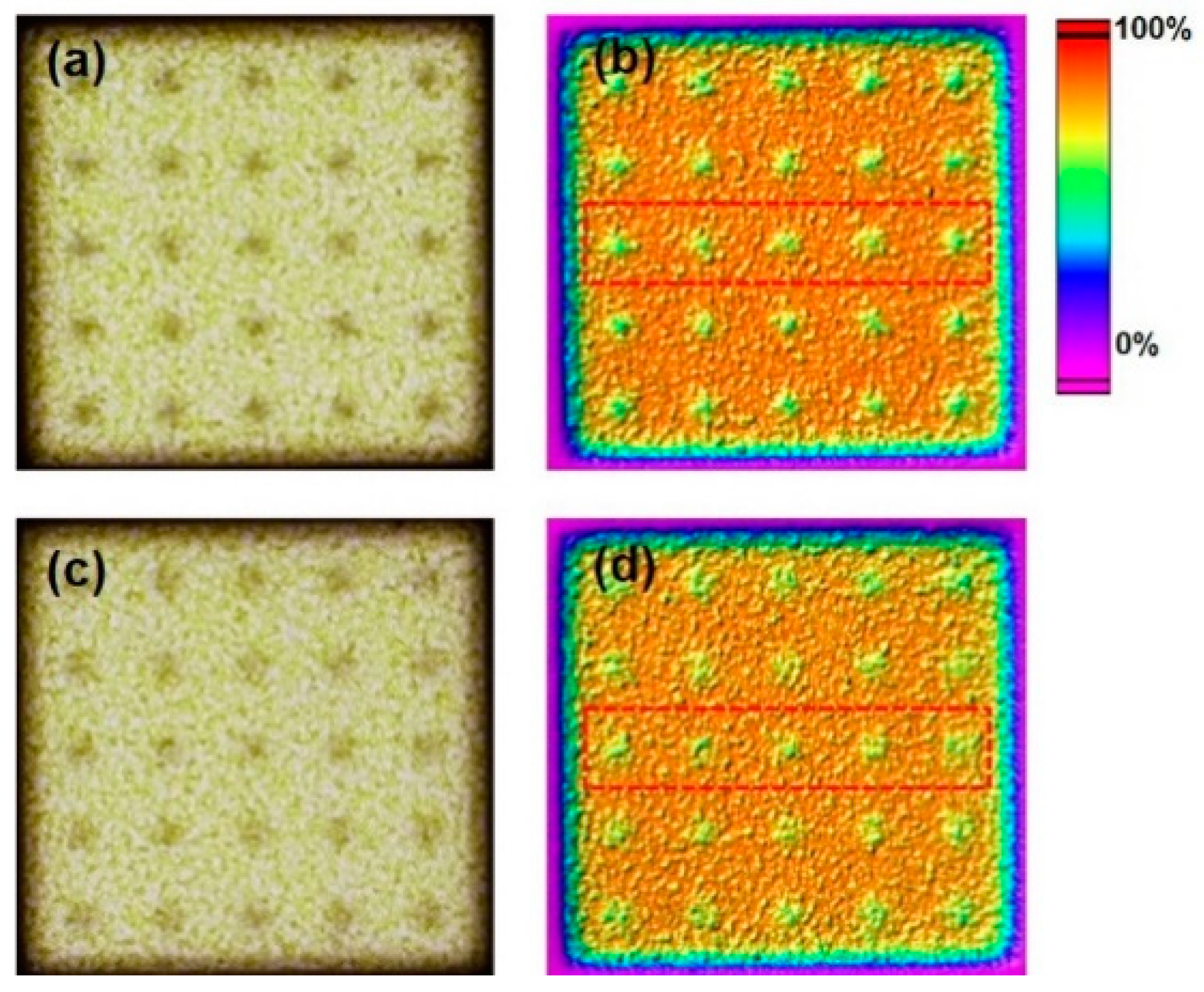
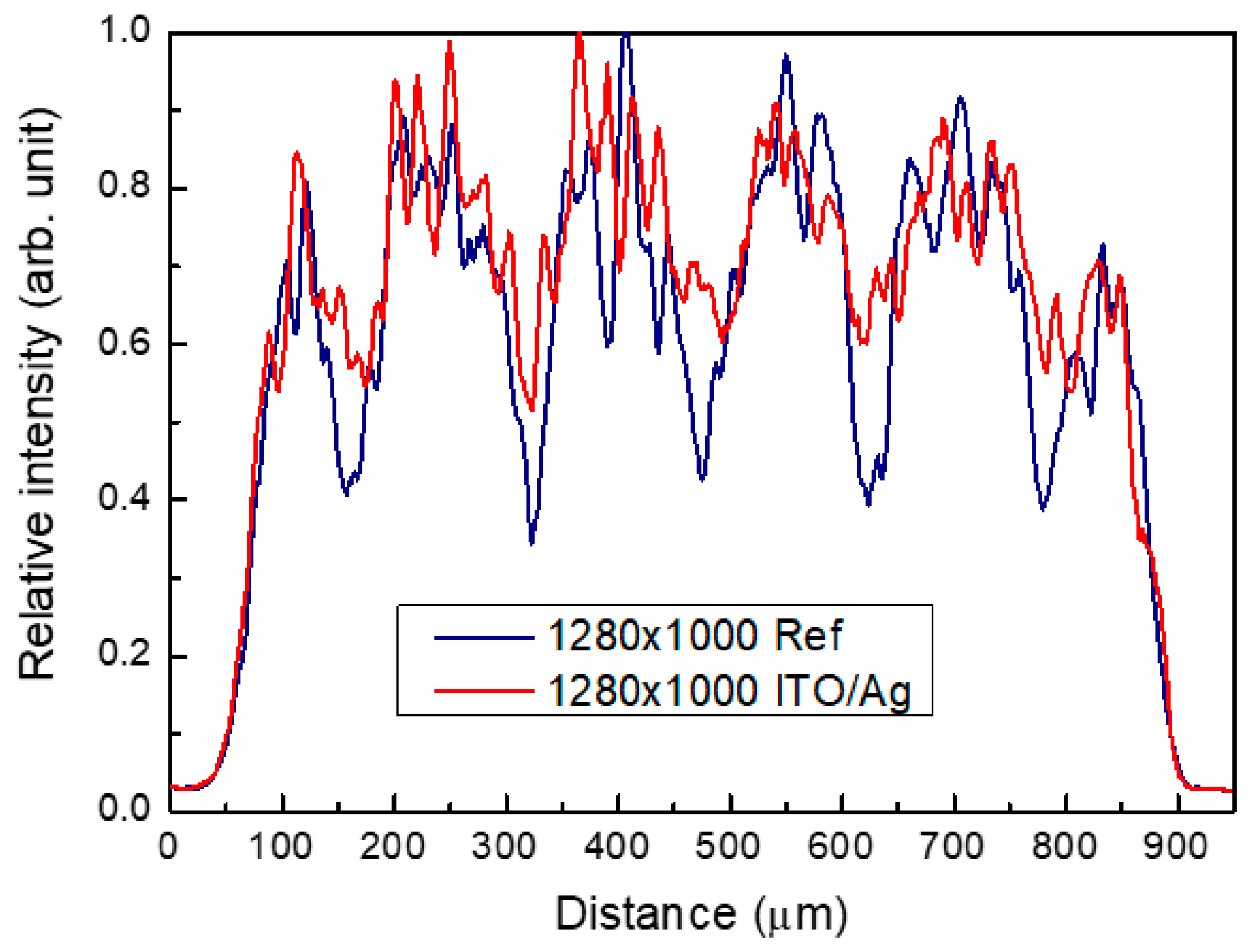
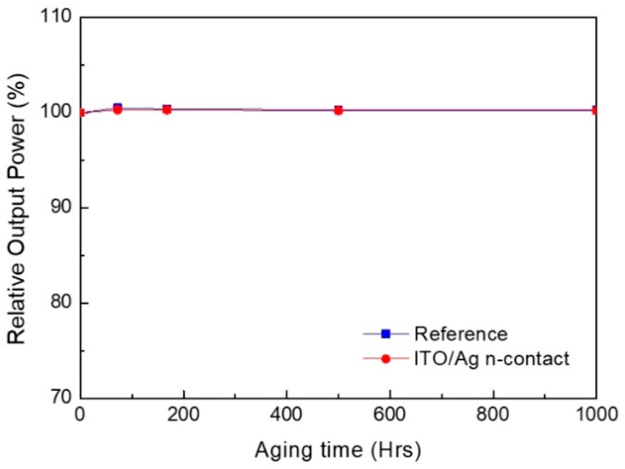
3. Results and Discussion

Optical microscope images of three different-size vertical-geometry LEDs (VLEDs) (size: 1280 × 1000 µm2, 1400 × 1400 µm2, and 1700 × 1700 µm2) with reference and ITO/Ag electrodes are shown in Figure 1. For the reference samples (Figure 1a,c,e), n-electrodes appear to be dark spots due to the opaque Ti/Al, whereas for the ITO/Ag-based samples (Figure 1b,d,f), there is almost no difference in the contrast because the ITO/Ag n-contact is the same as the underlying ITO/Ag p-reflector. To understand the effect of the number of n-contacts in the performance of vertical LEDs, the number of via holes (n-contacts) was varied from 25 (1280 × 1000 µm2) to 47 (1700 × 1700 µm2). Furthermore, the electroluminescence (EL) spectra at 350 mA of the VLEDs (1280 × 1000 µm2) with reference and ITO/Ag n-contact are displayed in Figure 1g. It is noted that both the samples show almost the same EL characteristic.
Figure 2 presents the I-V properties of fully packaged VLEDs as functions of n-contact schemes and chip size. It is shown that the forward voltage of the samples decreases with increasing chip size. For the reference samples, the forward voltage decreases from 3.38 to 3.20 V at 1500 mA, while the voltage of the ITO/Ag-based samples changes from 3.37 to 3.15 V. In addition, both the samples with reference and ITO/Ag contacts (1280 × 1000 µm2) showed the same series resistance of 2.3 Ω (below 100 mA). It is noted that regardless of chip size, the ITO/Ag-based samples produce forward voltages similar to the reference. This may be explained as follows. ITO is deposited by means of sputtering whose plasma process may damage the n-GaN, resulting in the generation of N vacancy and the effective removal of native oxide. This could improve the electrical property of n-type ohmic contact [22,23]. However, sputtering plasma could damage the electrical properties of p-GaN [24,25], resulting in an increase in the contact resistivity of p-type contacts and leading to high series resistance. Thus, the electrical property of p-type contacts dominates that of n-type contact and plays a dominant role in the forward voltages.
Figure 3 displays the light output-current relations of fully packaged VLEDs as functions of n-contact schemes and chip size. It is found that irrespective of chip size, the light output power of all samples increases with increasing current without saturation. Furthermore, the light output increases with increasing chip size. It is worth noting that regardless of chip size, the samples with the ITO/Ag contacts reveal higher light output power than the reference samples. For example, for the chip sizes of 1280 × 1000 µm2, 1400 × 1400 µm2, and 1700 × 1700 µm2, the ITO/Ag-based samples exhibit 2%, 2.5% and 3.4% higher light output power at 1500 mA than the reference samples, respectively. The higher output performance of the ITO/Ag-based samples can be explained as follows. Because of a large difference in the refractive indices of GaN and air, some amount of photons from the active region suffer from total internal reflection. These photons may be absorbed by opaque Ti/Al contact. However, for the ITO/Ag reflective contact, they can be redirected and extracted by the reflective Ag layer, leading to an increase in the light output. The volume fractions of the reflective regions (with reference to the whole active region) are estimated to be 90.9%, 93.6% and 94.6% for the Ti/Al-based samples with chip sizes of 1280 × 1000 µm2, 1400 × 1400 µm2, and 1700 × 1700 µm2, respectively, and 93.1%, 95.1% and 96.0% for the ITO/Ag-based samples (supplementary Figure S4). The volume fraction increases with increasing chip size and the ITO/Ag samples give higher volume fraction than the Ti/Al samples. Thus, the larger reflective region could result in higher light output. This can be confirmed by the light outputs of different-size VLEDs with the Ti/Al and ITO/Ag contacts at the same current density. For instance, for the chip sizes of 1280 × 1000 µm2, 1400 × 1400 µm2, and 1700 × 1700 µm2, the ITO/Ag-based samples produce 1.2%, 1.6% and 1.8% higher light output at 41~43 A/cm2 than the Ti/Al-based samples, respectively.
Figure 4 illustrates WPE of fully packaged VLEDs as functions of n-contact schemes and chip size. Regardless of n-contact schemes, the larger samples show higher WPE across the whole current range. Furthermore, irrespective of chip size, the WPE of all samples decreases with increasing current. However, the ITO/Ag-based samples undergo less degradation. For example, for the chip sizes of 1280 × 1000 µm2, 1400 × 1400 µm2, and 1700 × 1700 µm2, the ITO/Ag-based samples exhibit 2.3%, 3.1% and 4.8% higher WPE at 1500 mA than the reference samples, respectively. The WPE droop can be attributed to the combined effects of electron overflow, Auger recombination and Joule heating. It is shown that the overall current dependence is similar to that of light output power of the samples.
For thin film VLED structures, via holes for n-contacts are formed through the MQWs by dry etching, at which no photons are generated. The reference Ti/Al n-contacts having low reflectance absorb most of photons, whereas the ITO/Ag n-contacts effectively prevent the absorption of photons and could cause them to get extracted. Consequently, the n-contact regions appear dimmer than the surrounding area. Figure 5 shows plan-view light-emission and light intensity distribution images at 1.0 A obtained from the reference and ITO/Ag n-contact-based VLEDs (size: 1280 × 1000 µm2). As expected, the Ti/Al-based n-contacts appear darker than the ITO/Ag n-contacts, resulting in the non-uniformity of emission. This was further confirmed by line profiles, as illustrated in Figure 6, which were obtained from the regions (dotted squares) of the samples of Figure 5. The profiles show that the emission of the ITO/Ag n-contact regions is improved by 38.2% as compared with that of the reference (Ti/Al contact). So for the ITO/Ag-based sample, the ratio of the emission intensity of the active region (the surrounding area) and the contact areas is estimated to be 1.34. On the other hand, for the reference sample, the emission intensity ratio was 1.8. This indicates that the use of the ITO/Ag reflective n-contact effectively improves the emission uniformity. Here, the larger VLEDs (sizes: 1400 × 1400 µm2 and 1700 × 1700 µm2) are to show similar emission characteristics.
To examine the stability of packaged VLEDs with the ITO/Ag n-contact, the operation time dependence of the light output power was investigated. Figure 7 presents the light output power of fully packaged VLEDs (size: 1280 × 1000 µm2) with the reference and ITO/Ag-contacts as a function of operation time. The packaged samples that were attached to a heatsink were loaded into a chamber at 25 °C and stressed at current of 1.5 A. It is evidently shown that, like the reference sample, the ITO/Ag n-contact sample experiences no degradation after 1000 h. This implies that the ITO/Ag scheme can serve as a promising n-electrode for the fabrication of high-performance VLEDs for micro-LED-based display and vehicle headlamp applications.

4. Conclusions

The emission uniformity and light output of different chip-size VLEDs for VLED-based vehicle headlamp application were examined in terms of different n-type contacts and chip sizes. The forward voltage of both the samples decreased with increasing chip size from (1280 × 1000 µm2) to (1700 × 1700 µm2). Regardless of chip size, the ITO/Ag-based VLEDs revealed higher light output power than the Ti/Al-based reference samples. Irrespective of chip size, the WPE of all samples decreased with increasing current. However, the ITO/Ag-based samples suffered less degradation than the reference sample. It was observed that the ITO/Ag-based samples exhibited more uniform emission than the Ti/Al-based sample. Both the reference and ITO/Ag-based samples experienced no degradation after operation of 1000 h at 1500 mA. This implies that the ITO/Ag scheme can serve as a promising n-electrode for the fabrication of high performance VLEDs for vehicle headlamp applications.

Supplementary Materials

The following are available online at https://www.mdpi.com/article/10.3390/electronics10080975/s1, Figure S1: Fabrication process of vertical LEDs with (a) reference and (b) ITO/Ag contact. (c) Fabrication process after p-contact (the same for reference and ITO/Ag-LEDs), Figure S2: Schematic diagrams of vertical-geometry LEDs, Figure S3: Unlike conventional LEDs, square-shape active area and bar-like p-electrode were used for headlamp application in order to minimize dark space, Figure S4: The volume fractions of the reflective regions (with reference to the whole active region).

Author Contributions

Conceptualization, W.-S.Y. and Y.-K.J.; methodology, W.-S.Y., J.-H.K., D.-H.L. and Y.-H.K.; investigation, W.-S.Y., S.-Y.L. and S.-Y.J.; project management, Y.-K.J. and H.-H.J.; writing—original draft preparation, W.-S.Y. and T.-Y.S.; writing—review & editing, T.-Y.S.; Supervision, T.-Y.S. All authors have read and agreed to the published version of the manuscript.

Funding

This work was supported by the Global Research Laboratory (GRL) program through the National Research Foundation (NRF) of Korea (NRF-2017K1A1A2013160) and the Institute of Civil Military Technology Cooperation funded by the Defense Acquisition Program Administration.

Data Availability Statement

Not applicable.

Conflicts of Interest

The authors declare no conflict of interest.

References

  1. Kneissl, M.; Seong, T.-Y.; Han, J.; Amano, H. The emergence and prospects of deep-ultraviolet light-emitting diode technologies. Nat. Photon. 2019, 13, 233–244. [Google Scholar] [CrossRef]
  2. Lee, B.-R.; Park, J.-H.; Kim, T.-G. Micro-light-emitting diode with n-GaN/NiO/Au-based resistive-switching electrode for compact driving circuitry. J. Alloys Compd. 2020, 823, 153762. [Google Scholar] [CrossRef]
  3. Song, J.-O.; Kwak, S.; Seong, T.-Y. Cu-doped indium oxide/Ag ohmic contacts for high-power flip-chip light-emitting diodes. Appl. Phys. Lett. 2005, 86, 062103. [Google Scholar] [CrossRef]
  4. Weisbuch, C. On The Search for Efficient Solid State Light Emitters: Past, Present, Future. ECS J. Solid State Sci. Technol. 2020, 9, 016022. [Google Scholar] [CrossRef]
  5. Hu, X.-L.; Xiao, F.-A.; Zhou, Q.-B.; Zheng, Y.-D.; Liu, W.-J. High-luminous efficacy green light-emitting diodes with InGaN/GaN quasi-superlattice interlayer and Al-doped indium tin oxide film. J. Alloys Compd. 2019, 794, 137–143. [Google Scholar] [CrossRef]
  6. Song, J.-O.; Kwak, S.; Park, Y.; Seong, T.-Y. Improvement of the light output of InGaN-based light-emitting diodes using Cu-doped indium oxide/indium tin oxide p-type electrodes. Appl. Phys. Lett. 2005, 86, 213505. [Google Scholar] [CrossRef]
  7. Jang, J.-S.; Park, S.-J.; Seong, T.-Y. Metallisation scheme for highly low-resistance, transparent, and thermally stable ohmic contacts to p-GaN. Appl. Phys. Lett. 2000, 76, 2898. [Google Scholar] [CrossRef] [Green Version]
  8. Taki, T.; Strassburg, M. Visible LEDs: More than Efficient Light. ECS J. Solid State Sci. Technol. 2020, 9, 015017. [Google Scholar] [CrossRef]
  9. Chu, J.-T.; Huang, H.-W.; Kao, C.-C.; Liang, W.-D.; Lai, F.-I.; Chu, C.-F.; Kuo, H.-C.; Wang, S.-C. Fabrication of Large-Area GaN-Based Light-Emitting Diodes on Cu Substrate. Jpn. J. Appl. Phys. 2005, 44, 2509–2511. [Google Scholar] [CrossRef]
  10. Uang, K.-M.; Wang, S.-J.; Chen, S.-L.; Yang, Y.-C.; Chen, T.-M.; Liou, B.-W. Effect of Surface Treatment on the Performance of Vertical-Structure GaN-Based High-Power Light-Emitting Diodes with Electroplated Metallic Substrates. Jpn. J. Appl. Phys. 2006, 45, 3436–3441. [Google Scholar] [CrossRef]
  11. Lee, S.Y.; Choi, K.K.; Jeong, H.-H.; Choi, H.S.; Oh, T.-H.; Song, J.O.; Seong, T.-Y. Wafer-level fabrication of GaN-based vertical light-emitting diodes using a multi-functional bonding material system. Semicond. Sci. Technol. 2009, 24, 092001. [Google Scholar] [CrossRef]
  12. Haerle, V.; Hahn, B.; Kaiser, S.; Weimar, A.; Bader, S.; Eberhard, F.; Plössl, A.; Eisert, D. High brightness LEDs for general lighting applications Using the new ThinGaN™-Technology. Phys. Status Solidi A 2004, 201, 2736–2739. [Google Scholar] [CrossRef]
  13. Kim, H.; Choi, K.-K.; Kim, K.-K.; Cho, J.; Lee, S.-N.; Park, Y.; Kwak, J.S.; Seong, T.-Y. Light-extraction enhancement of vertical-injection GaN-based light-emitting diodes fabricated with highly integrated surface textures. Opt. Lett. 2008, 33, 1273–1275. [Google Scholar] [CrossRef]
  14. Shchekin, O.B.; Epler, J.E.; Trottier, T.A.; Margalith, T.; Steigerwald, D.A.; Holcomb, M.O.; Martin, P.S.; Krames, M.R. High performance thin-film flip-chip InGaN–GaN light-emitting diodes. Appl. Phys. Lett. 2006, 89, 071109. [Google Scholar] [CrossRef]
  15. Laubsch, A.; Sabathil, M.; Baur, J.; Peter, M.; Hanh, B. High-Power and High-Efficiency InGaN-Based Light Emitters. IEEE Trans. Electron Devices 2010, 57, 79–87. [Google Scholar] [CrossRef]
  16. Han, J.; Lee, D.; Jin, B.; Jeong, H.; Song, J.O.; Seong, T.-Y. Optimizing n-type contact design and chip size for high-performance indium gallium nitride/gallium nitride-based thin-film vertical light-emitting diode. Mater. Sci. Semicond. Process 2015, 31, 153–159. [Google Scholar] [CrossRef]
  17. Luther, B.P.; Mohney, S.E.; Jackson, T.N.; Asif Khan, M.; Chen, Q.; Yang, J.W. Investigation of the mechanism for Ohmic contact formation in Al and Ti/Al contacts to n-type GaN. Appl. Phys. Lett. 1997, 70, 57–59. [Google Scholar] [CrossRef] [Green Version]
  18. Lin, M.E.; Ma, Z.; Huang, F.Y.; Fan, Z.F.; Allen, L.H.; Morkoc, H. Low resistance ohmic contacts on wide band-gap GaN. Appl. Phys. Lett. 1994, 64, 1003–1005. [Google Scholar] [CrossRef]
  19. Lester, L.F.; Brown, J.M.; Ramer, J.C.; Zhang, L.; Hersee, S.D.; Zolper, J.C. Nonalloyed Ti/Al Ohmic contacts to n-type GaN using high-temperature premetallization anneal. Appl. Phys. Lett. 1996, 69, 2737–2739. [Google Scholar] [CrossRef]
  20. Kim, T.K.; Cho, M.U.; Lee, J.M.; Cha, Y.-J.; Oh, S.K.; Chatterjee, B.; Ryou, J.-H.; Choi, S.; Kwak, J.S. Improved Light Output Power of 16×16 Pixelated Micro-LEDs for Headlights by Enhancing the Reflectivity and Coverage of the p-Electrode. Phys. Status Solidi A 2018, 215, 1700571. [Google Scholar] [CrossRef]
  21. Takahashi, Y.; Kita, Y.; Uchida, M. Development of 288segments matrix ADB system with improved visibility and safety. In Proceedings of the 12th international Symposium on Automotive Lighting, Darmstadt, Germany, 21 August 2017; p. 323. [Google Scholar]
  22. Kim, D.W.; Lee, H.Y.; Sung, Y.J.; Yeom, G.Y. A study of transparent contact to vertical GaN-based light-emitting diodes. J. Appl. Phys. 2005, 98, 053102. [Google Scholar] [CrossRef]
  23. Hwang, J.D.; Yang, G.H.; Chang, W.T.; Lin, C.C.; Chuang, R.W.; Chang, S.J. A novel transparent ohmic contact of indium tin oxide to n-type GaN. Microelectron. Eng. 2005, 77, 71. [Google Scholar] [CrossRef]
  24. Song, J.O.; Ha, J.S.; Seong, T.-Y. Ohmic-Contact Technology for GaN-Based Light-Emitting Diodes: Role of P-Type Contact. IEEE Trans. Electron. Devices 2010, 57, 42–59. [Google Scholar] [CrossRef]
  25. Götz, W.; Johnson, N.M.; Walker, J.; Bour, D.P.; Street, R.A. Activation of acceptors in Mg-doped GaN grown by metalorganic chemical vapor deposition. Appl. Phys. Lett. 1996, 68, 667. [Google Scholar] [CrossRef]
Figure 1. Optical microscope images of three different-size VLEDs (chip sizes of (a,b) 1280 × 1000 µm2, (c,d) 1400 × 1400 µm2, and (e,f) 1700 × 1700 µm2) with (a,c,e) reference and (b,d,f) ITO/Ag electrodes. (g) EL spectra of the VLEDs (1280 × 1000 µm2) with reference and ITO/Ag n-contact.
Electronics 10 00975 g001
Figure 2. The I-V properties of fully packaged VLEDs as functions of n-contact schemes and chip size.
Electronics 10 00975 g002
Figure 3. The light output–current relations of fully packaged VLEDs as functions of n-contact schemes and chip size.
Electronics 10 00975 g003
Figure 4. The WPE of fully packaged VLEDs as functions of n-contact schemes and chip size.
Electronics 10 00975 g004
Figure 5. Plan-view (a,c) light-emission and (b,d) light intensity distribution images at 1.0 A which were obtained from (a,b) the reference and (c,d) ITO/Ag n-contact VLEDs (size: 1280 × 1000 µm2).
Electronics 10 00975 g005
Figure 6. Line profiles of the emission images from the reference and ITO/Ag n-contact VLEDs, which were obtained from the regions (dotted squares) of the samples of Figure 5.
Electronics 10 00975 g006
Figure 7. The light output power of fully packaged VLEDs (size: 1280 × 1000 µm2) with the reference and ITO/Ag-contacts as a function of operation time.
Electronics 10 00975 g007
Publisher’s Note: MDPI stays neutral with regard to jurisdictional claims in published maps and institutional affiliations.

