Article

A Study to Resist Conduced Interference from GIS Bus-Charging Currents Switching for Electronic Current Transformer

1
State Key Laboratory of Electrical Insulation and Power Equipment, Xi’an Jiaotong University, Xi’an 710049, China
2
Xi’an XD High Voltage Appapatus Co., Ltd., Xi’an 710077, China
*
Author to whom correspondence should be addressed.
Electronics 2021, 10(8), 957; https://doi.org/10.3390/electronics10080957
Submission received: 17 March 2021 / Revised: 10 April 2021 / Accepted: 12 April 2021 / Published: 16 April 2021
(This article belongs to the Special Issue Electromagnetic Interference and Compatibility, Volume II)

Abstract

:
In this paper, we study the conducted interference to an electronic current transformer introduced in the process of bus-charging currents which are caused by switching a gas insulated switchgear (GIS) disconnector. To cope with these issues, the EMTP-ATP and Matlab/Simulink software are used to carry out equivalent modeling simulations and experimental research, respectively. More specifically, the very fast transient current generated by disconnector switching (DS) is used as the input source of the equivalent simulation model of the Rogowski coil, and the characteristics of conducted interference waveforms of the Rogowski coil, the active integrator and filter outputs under single and multiple breakdowns are analyzed step by step. Moreover, several anti-interference methods are proposed to improve the resistance to the high-voltage and high-frequency conducted interference for the Rogowski coil, such as reducing the Rogowski cut-off frequency, increasing the transient voltage suppressor (TVS), active filter, and Cy capacitor. Besides, the study also reveals that the residual charge of the integral capacitor will discharge with a time constant τ = 1 s after arc quenching with the first-order discharge circuit, which is composed of the feedback resistance and the integral capacitor C. Lastly, the experimental results demonstrate the correctness of the modeling method proposed in this paper and the effectiveness of anti-interference measures.

1. Introduction

It is known that very fast transient overvoltage (VFTO) and very fast transient current (VFTC) can be generated frequently by multiple prestrikes and restrikes when the disconnector in air insulated switchgear (AIS) or GIS switches capacitive load. However, they both have a serious impact on the reliability of primary insulation and secondary equipment [1,2]. Particularly, the amplitude of VFTC can reach up to several thousand amperes, causing sudden changes in the current signal and strong electromagnetic interference [3,4]. Furthermore, the GIS ECT sensor is highly integrated with GIS, and sampling units are installed on the enclosure or chassis of GIS, which is in a bad electromagnetic environment [5]. Moreover, the GIS ECT sensor, which is more susceptible to the fast transient electromagnetic interference in the process of disconnector switch operation, can cause the change of the ECT accuracy level, intermittent operation failure, and even permanent damage and failure of devices [6,7].
Recently, the reduction of the damage to electronic current transformers caused by the disconnector switch operation has aroused the attention of researchers. In [8], the combination of RC filter and TVS is utilized to improve the anti-interference performance of the transformer. Additionally, the signal waveform under the influence of VFTO is obtained by establishing the high-frequency transient model of the Rogowski coil of the electronic current transformer [9], where the distributed parameter model is proved that it can reflect the high-frequency characteristics by comparing the waveform of distribution parameter model, lumped parameter model and the measured signal waveform. The authors of [10] proposed that the design and application of the GIS electronic current transformer is a systematic process, which indicates that it is necessary to consider the overall design of the GIS, the suppression of VFTO in the GIS structure layout, buses, the size of the shell and the well-earthing, and other factors. In [11], the reasons of the acquisition card malfunction are deeply analyzed, and some specific anti-interference measures are implemented in many aspects, such as the installation position of the electronic transformer acquisition box, the grounding mode, the protection of the signal port, and so on. Beyond above, the author of [12] calculates the peak amplitude of VFTC and their dominant frequency content in a 245 kV GIS at various locations for different switching operations and substation configurations, which also gives the influence of the substation layout on the spectrum, dominant frequencies and the highest possible frequency components of VFTC with different distances from the switch. In [13], it is proposed that adding a damping resistance can greatly improve the attenuation speed of the VFTC, which is beneficial for the suppression of VFTC, but the damping resistance has little impact on the main frequency distribution.
Despite the progress reported in the above references, there are some common problems in the current research on conducted interference of electronic current transformers: (1) the cut-off frequency of the Rogowski coil exceeds 100 kHz, even up to 1 MHz, but the protection of the power frequency system only needs 1–13 harmonics. Under this setting, an unreasonable parameter design can cause serious waste and may fail to effectively attenuate the VFTC from the perspective of the sensor. (2) It is not reasonable to use the zero-crossing point of the VFTC as the signal of arc extinction in simulations. General studies have shown that the arc extinction depends on the moment when the VFTC attenuation approaches zero, rather than the moment of the current zero-crossing. (3) Most studies concentrate on the waveform characteristics of the Rogowski coil output or the final output waveform characteristics of the merging unit, but only a few introduce TVS and RC filtering suppression. The response waveform characteristics of key transmission nodes in the intermediate sampling unit have not been studied in detail. (4) Most of the isolation switches use spring mechanisms, and the switching speed is 0.54–3.5 m/s, which has a less practical value compared with most low-speed electric mechanisms used in practical engineering. (5) The test target of switching capacitive current is not a GIS with a complete interval and ECT in practical engineering, but a simplified equivalent test circuit.
To solve the above problems, we choose to carry out simulations of conduction interference to electronic current transformer, in which the VFTC is caused by switching the capacitive load of the disconnector. Moreover, specific anti-interference measures are also put forward to overcome above problems. Lastly, an experimental study on disconnector switching small capacitive current is carried out to verify the effectiveness of our proposed anti-interference measures and to evaluate the correctness of the simulation model.
To sum up, the main contributions of our work are as follows.
  • The cut-off frequency of the Rogowski coil is reduced as much as possible, and the VFTC with high frequency and high amplitude is attenuated effectively.
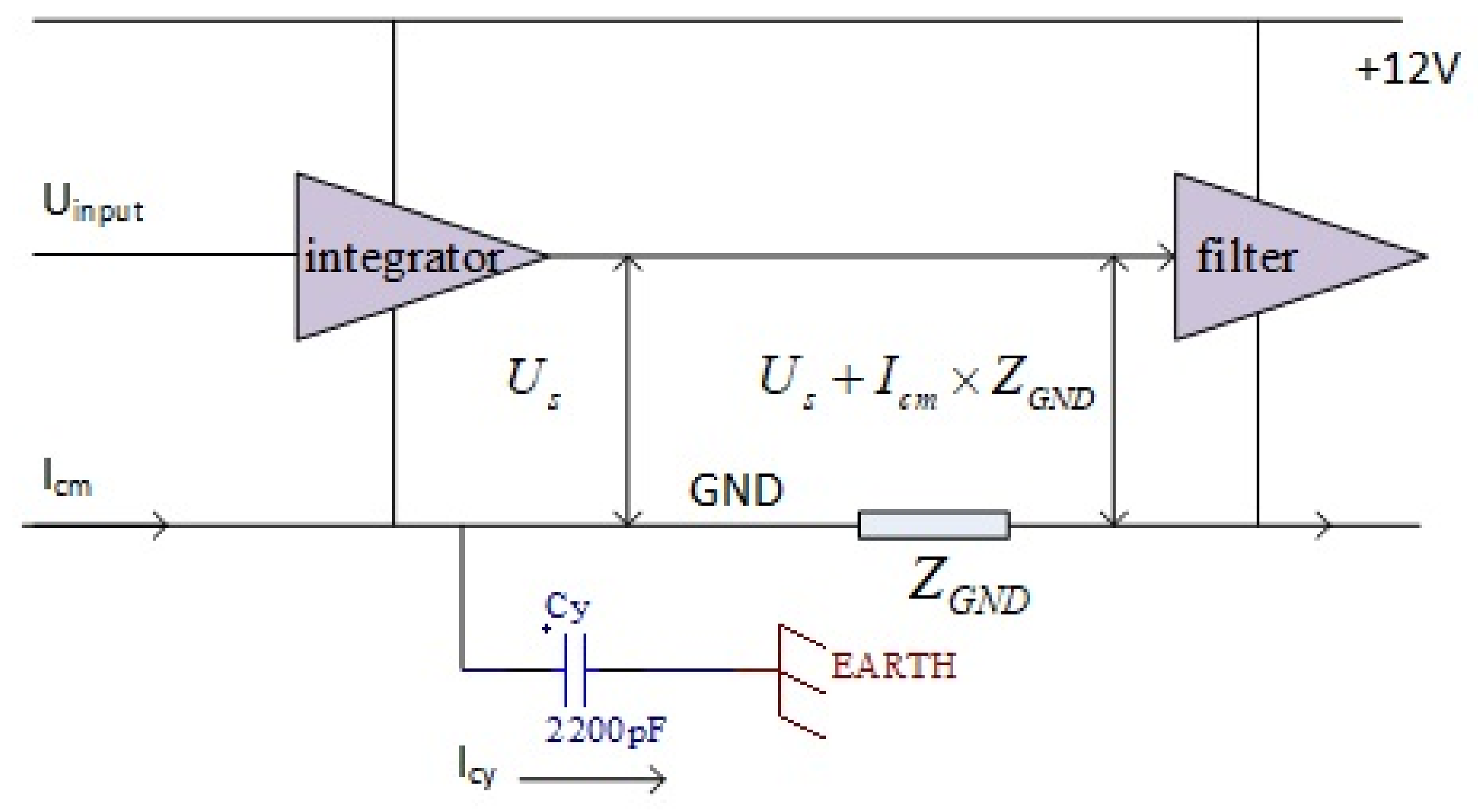
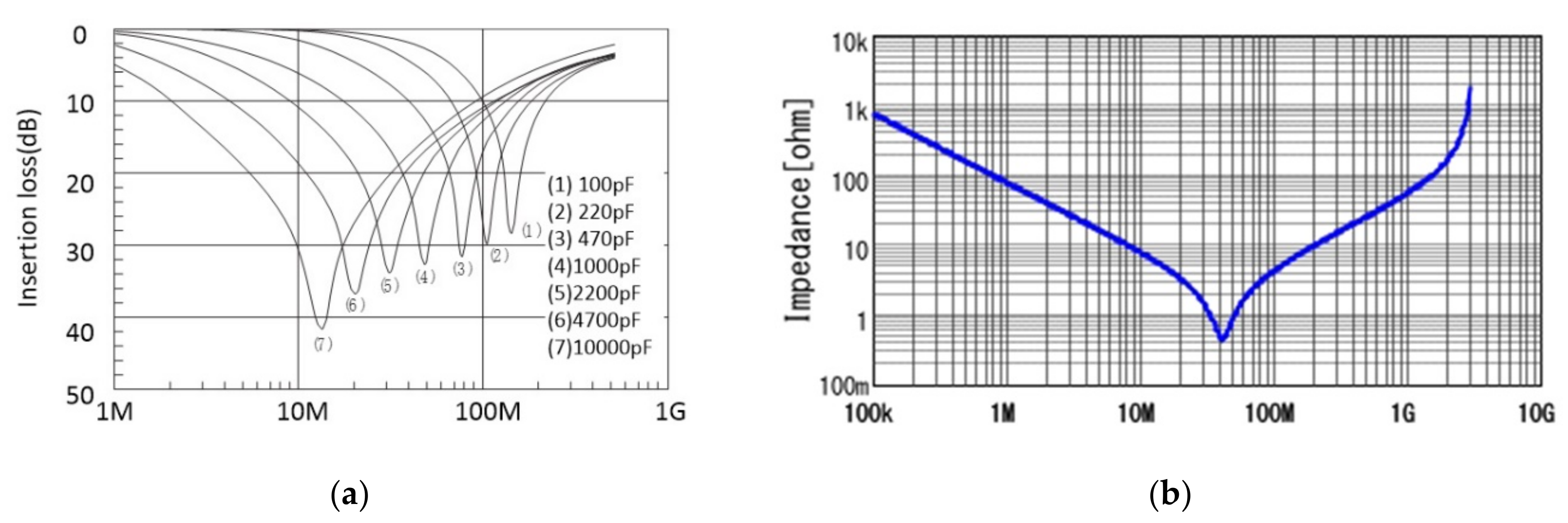
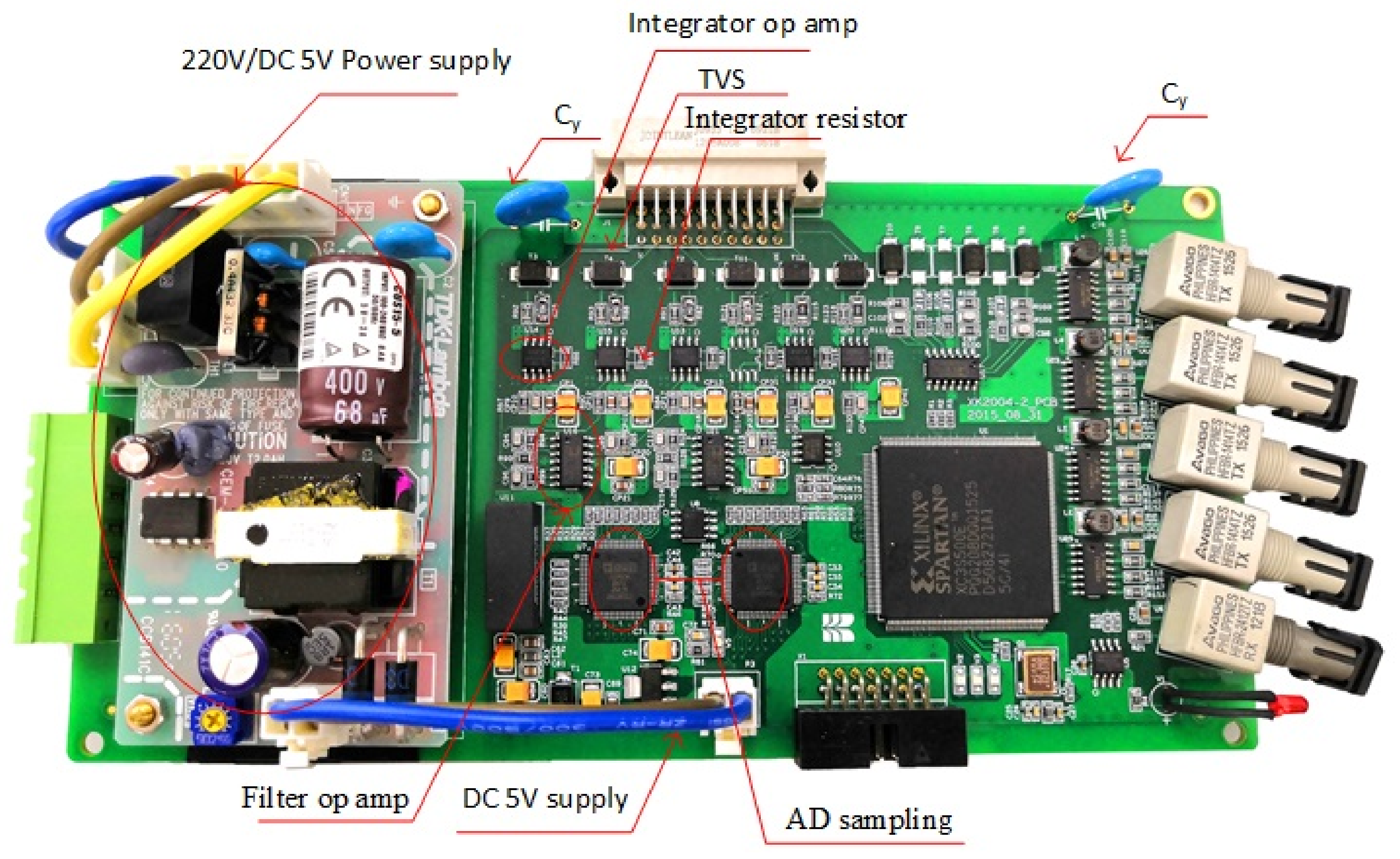
  • A TVS and an active filter are added to suppress the conducted interference with high frequency and high amplitude, and the Cy capacitor is used to solve the problem of PCB ground interference. A detailed method is also provided, which can design and calculate the cut-off frequency of the Rogowski coil and the parameter selection of the TVS, the filter and Cy capacitance in the sampling unit.
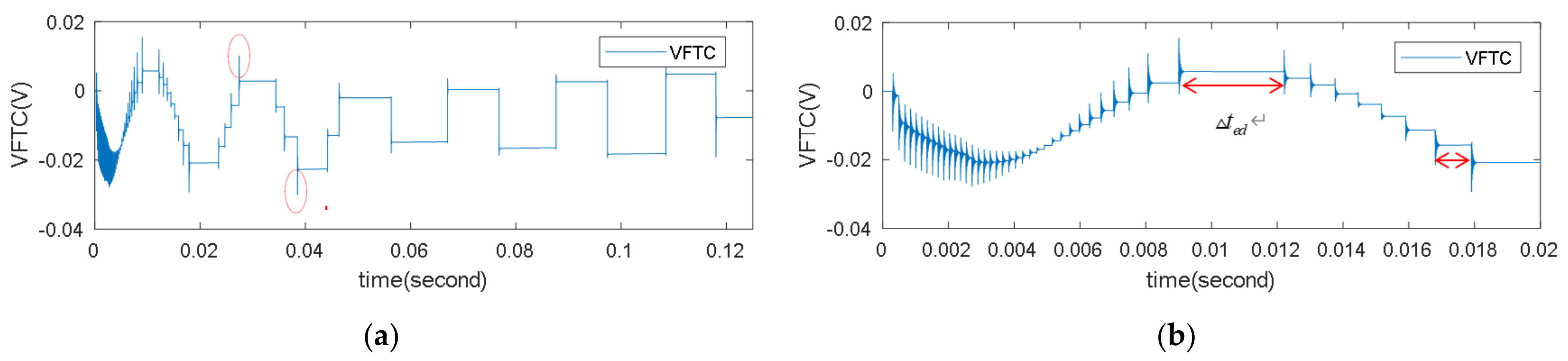
  • The arc extinction is judged by VFTC attenuation to zero instead of the VFTC zero-crossing.
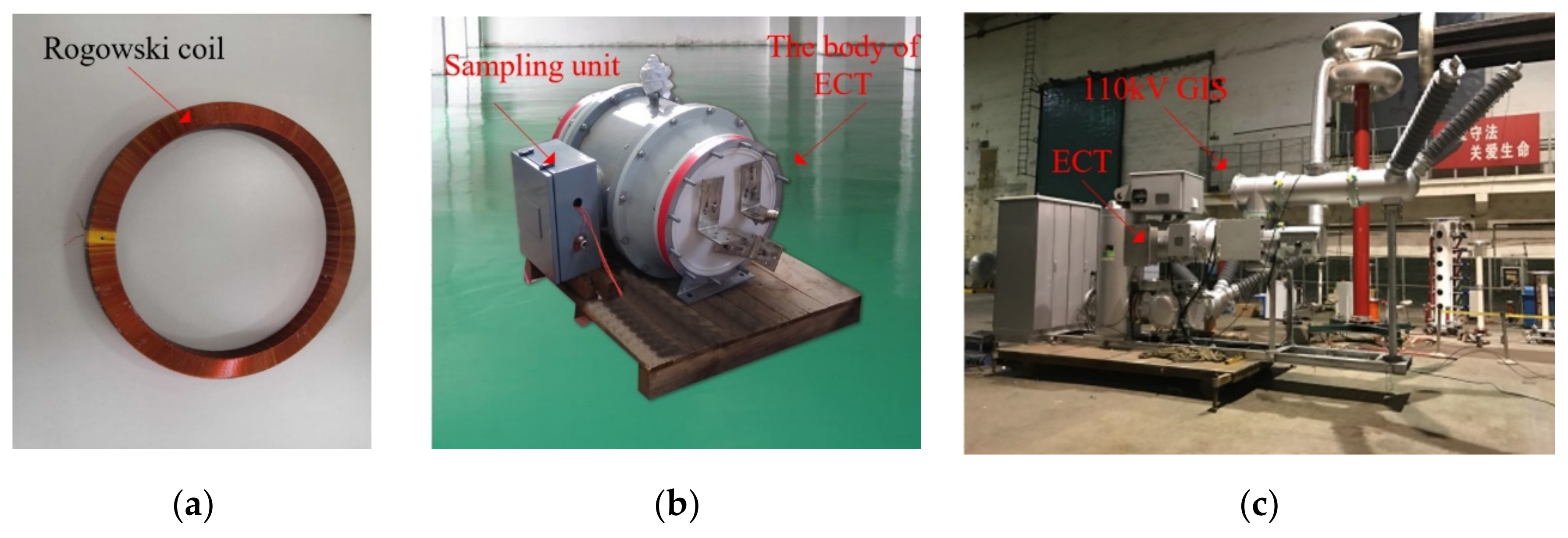
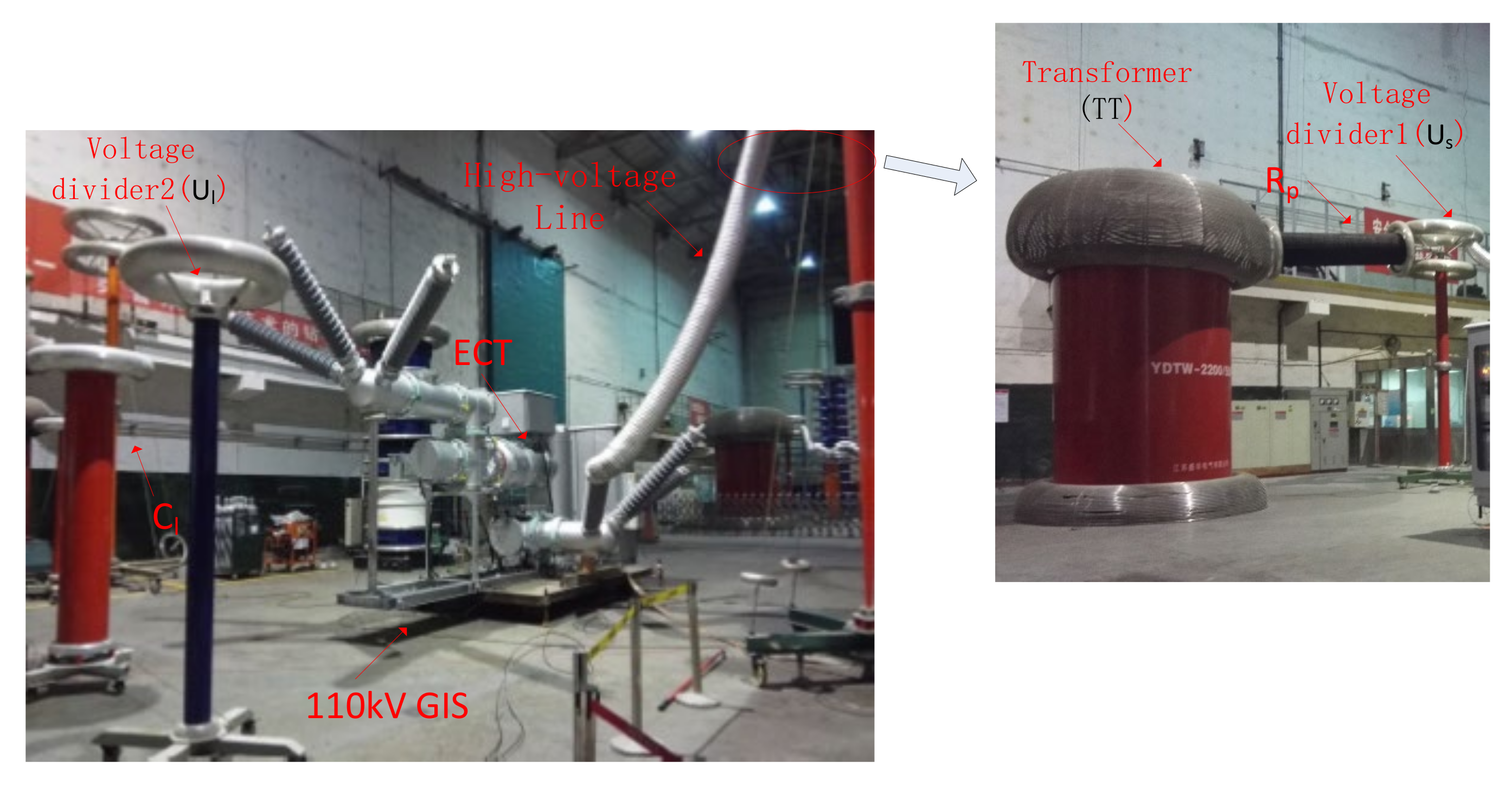
  • The complete GIS interval installed with the ECT is connected to the experimental circuit, which makes our experiment more in line with the practical application of engineering.
This paper has five parts: Section 1 is the Introduction; Section 2 introduces the GIS disconnector switching circuit and the electronic current transformer simulation model; Section 3 presents the simulation result analysis; Section 4 shows the switching small capacitive current test of the disconnector. Finally, the conclusions and prospects of this paper are given in Section 5.

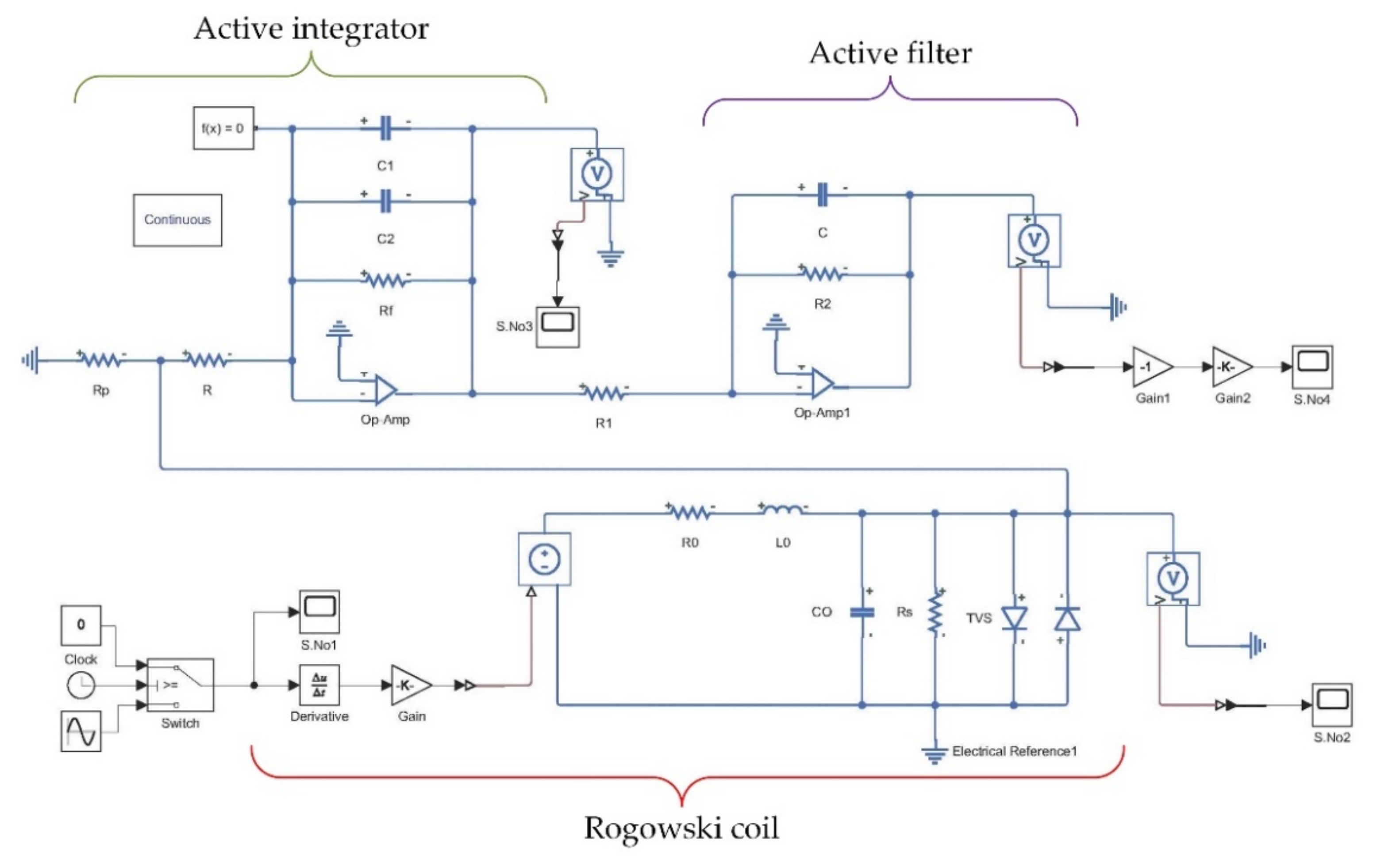
2. Simulation Models of GIS Disconnector Switching Circuit and Electronic Current Transformer

The VFTO generated due to the disconnector switch operations in GIS and the associated VFTC could have a rise time ranging from 4 to 7 ns [14]. Compared with the VFTO, in addition to the characteristics described in the literature [15,16,17], the VFTC in the GIS bus will be directly transmitted to the input of the unit through the Rogowski coil of the electronic current transformer, causing sufficiently severe harm to the sampling unit and other equipment and disrupting its stable operation.

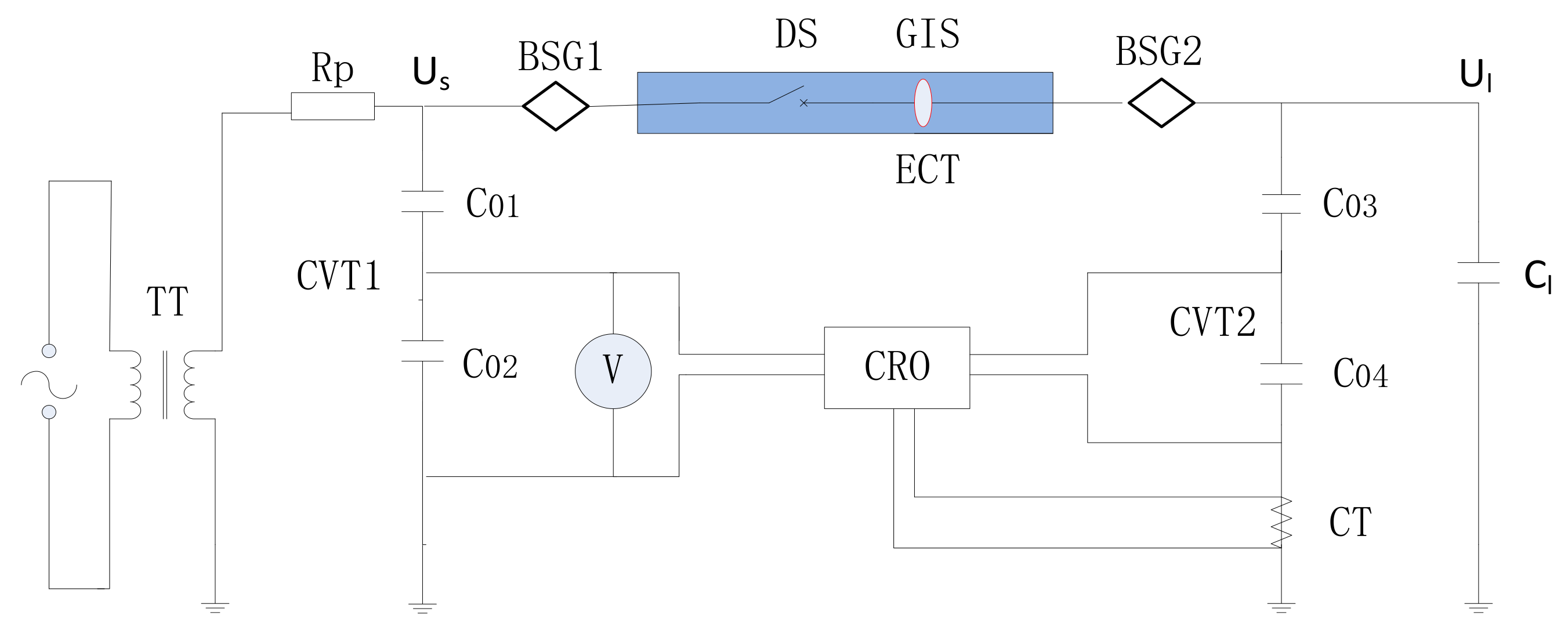
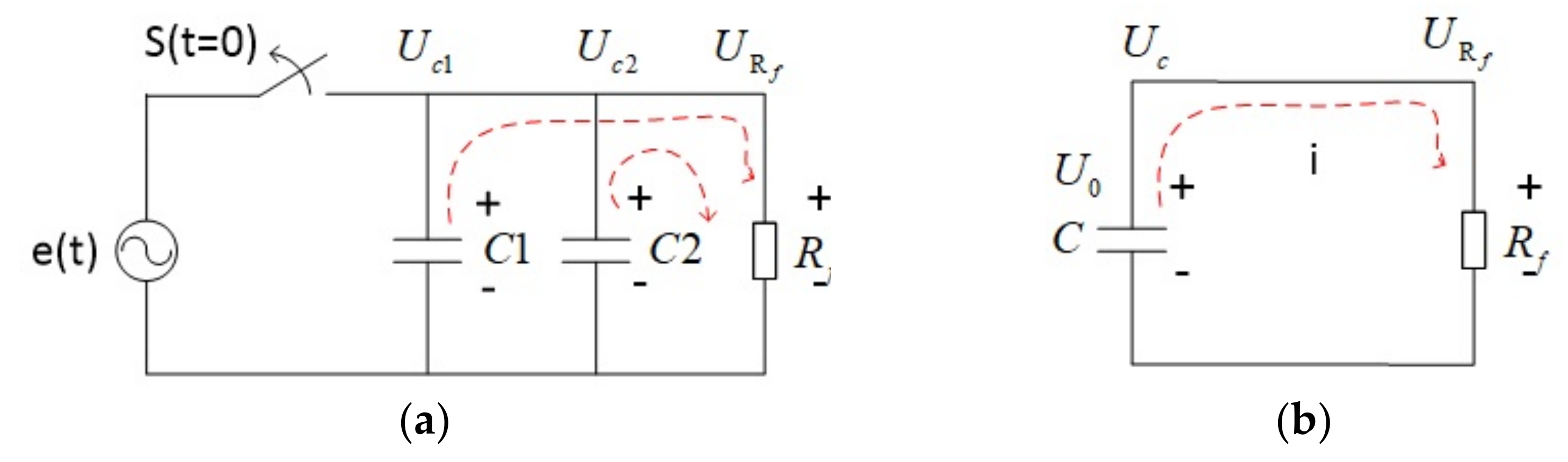
2.1. Connection Modes of Test Circuit

The State Grid Corporation of China suggested that the charging current test of the disconnector switch bus should be carried out in accordance with the test duty 3 in GB1985-2004 in the intelligent GIS test scheme. This paper therefore takes the test duty 3 of the GIS disconnector switching bus-charging currents as the research object [18,19,20,21] and performs simulations and an experimental verification of the conduction interference of VFTC to ECT generated during the GIS disconnector opening and closing process. Referring to the IEC62271-102-2001 standard [22], the connection mode of the test duty 3 of bus-charging currents switching by the GIS disconnector is built as shown in Figure 1. The DS in the GIS is a test disconnector switch used to open and close C1 on the load side to generate the VFTO and VFTC. The VFTC generated by the operation is sensed and conducted by the ECT installed on the GIS with the Rogowski coil principle [23,24]. CVT1 and CVT2 are capacitive voltage dividers, which measure the voltage on the power supply side and load side, respectively. The main parameters of the test circuit are shown in Table 1.

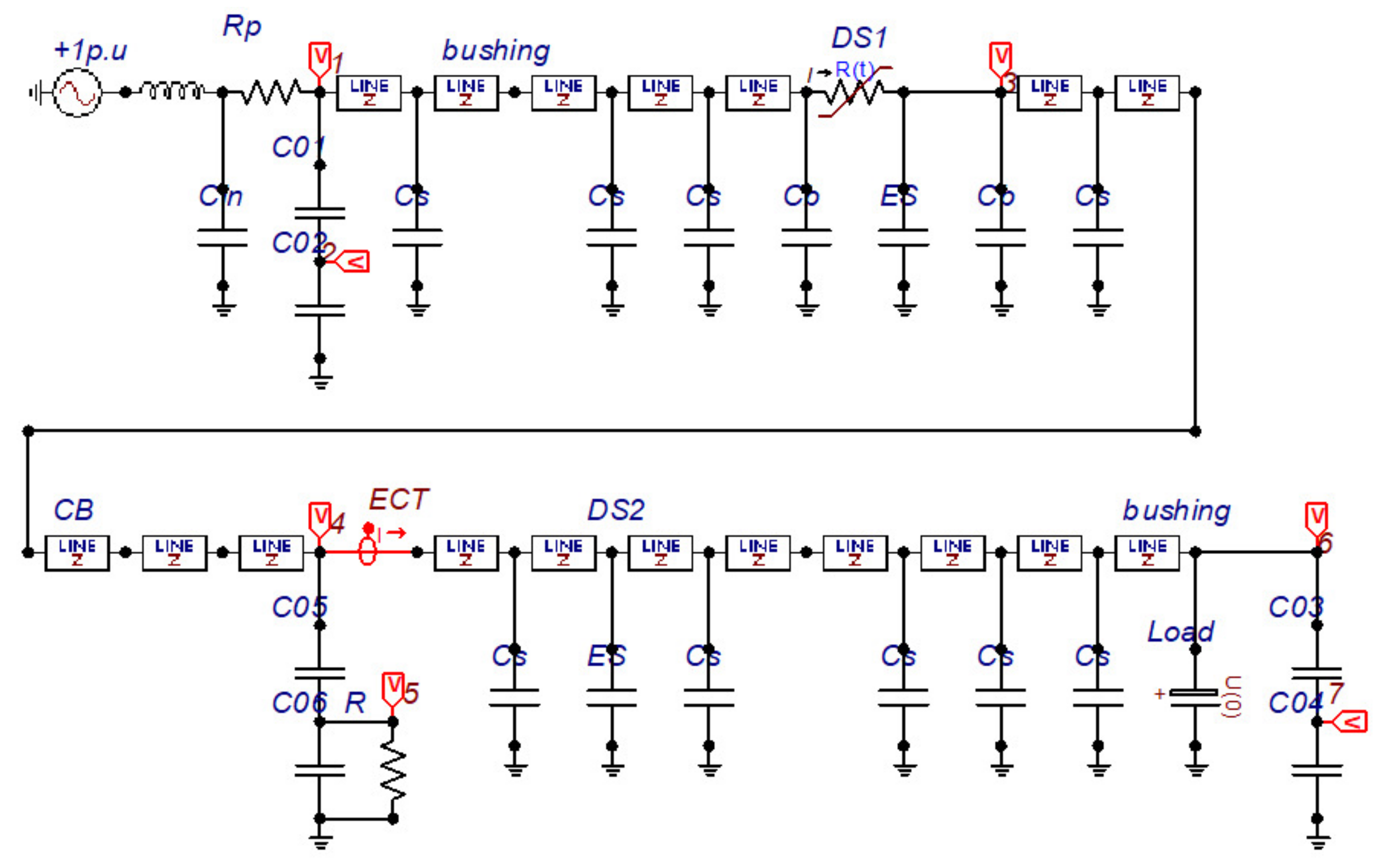
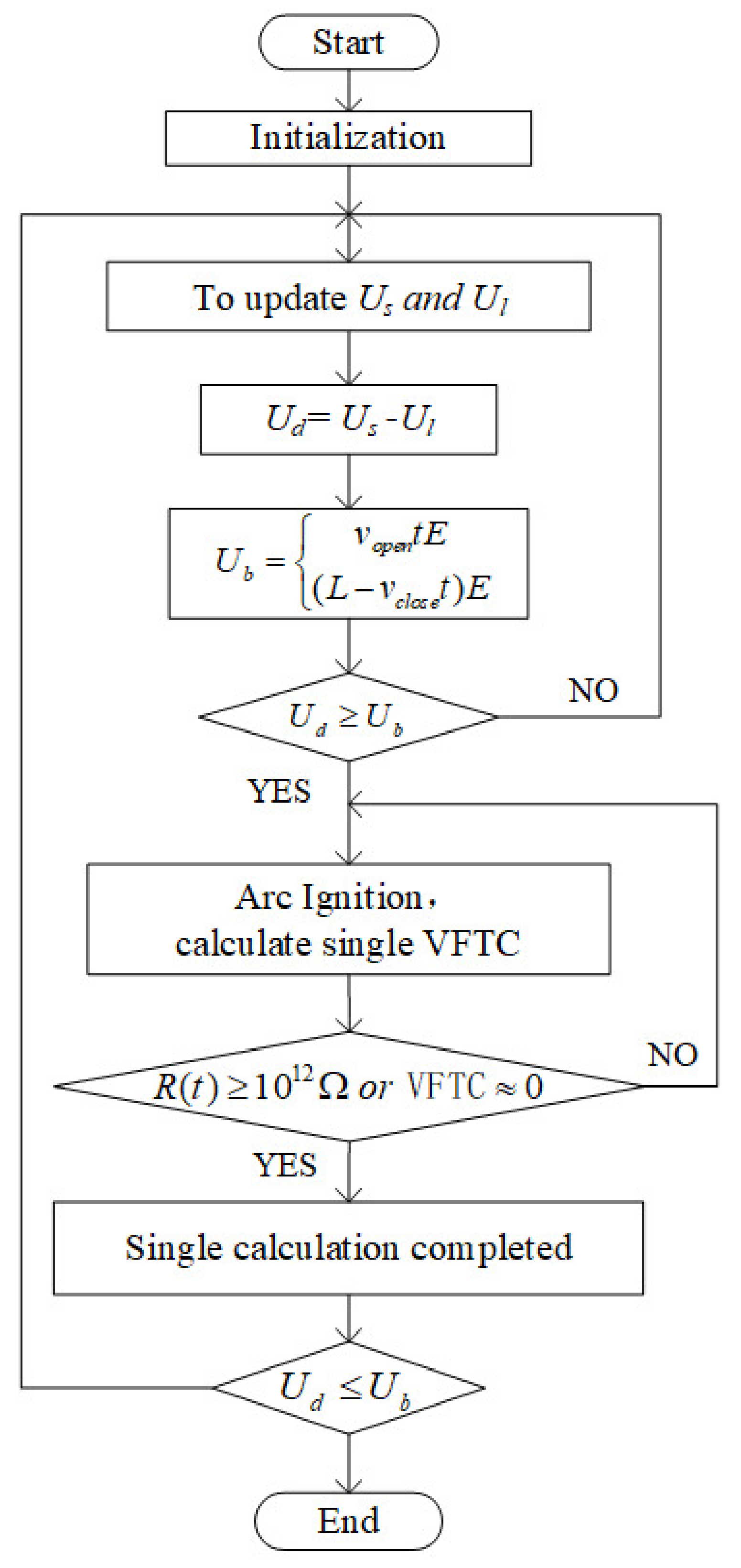
2.2. High-Frequency Simulation Model of VFTC Generated by GIS Disconnector Switching

In this paper, we chose the three-phase enclosed 110 kV GIS for the VFTC studies. Table 2 gives the electrical equivalent representation of various GIS components and includes sources and loads components [25,26,27,28,29,30].
The typical length of a GIS bus is much smaller than that of an ordinary substation, and in the high frequency range from hundreds of kHz to MHz, the GIS bus acts like a transmission line, with limited transit time, propagation speed, and surge impedance. Therefore, the GIS bus is modeled as a transmission line with the surge impedance value as follows:
Z = 60 ln ( b a )
where a is the diameter of the high voltage bus and b is the inner diameter of the enclosure. For the 110 kV GIS model, the surge impedance value is found to be between 40–90 Ω. The arc resistance model R(t) adopts the form of the double exponential function [25], as follows:
R ( t ) = R 1 ( t ) + R 2 ( t ) = R e t / τ 1 i + R e t / τ 2 c
where Ri is the insulation resistance of isolating switch port before the breakdown, which is about 1012 Ω; τ1 is the time constant of the breakdown period, which is about 1 ns and τ2 is the recovery time constant, which is about 1 μs; Rc is the arc resistance during the arc period. As can be seen in Figure 2, we establish the transient process circuit model of the GIS disconnector switching capacitive bus in the EMTP-ATP software.
It can be seen from reference [31] that the high frequency oscillating arc current VFTC determines the extinction of the arc between disconnector contacts. The arc will be extinguished (R(t) ≥ 1012) only when the high-frequency oscillation current VFTC attenuates to zero, otherwise the arc-burning process will continue. Thus, the parameters of the arc current id and the arc resistance R(t) should be comprehensively considered when judging the reignition and extinguishment of the arc. The calculation flow of the simulation model for the VFTC generated by the disconnector switching is described in Figure 3. According to the reference [32], the breakdown voltage Ub of the GIS disconnector gap is a function of time t, which can be simplified as follows:
U b = v o p e n t E ( L v c l o s e t ) E
where vopen and vclose are the average moving speeds of switch contacts for opening and closing, respectively, E is the withstand voltage per unit length of the switch gap; L represents the gap distance when the disconnector is opened, and t is time. Table 3 gives the electrical parameters of the isolating switch and the breakdown time can be obtained according to the time when UdUb. As in Equation (3), the arc will be extinguished when the arc resistance reaches 1012 Ω or when id ≈ 0, and then the time of the arc extinguishment as well as the corresponding bus residual voltage Ul can be obtained.
Figure 3 gives the simple flow chart for the whole process simulation of the VFTC generated during the disconnector switching [33,34]. The switching speed of the disconnector is slow, and it takes about 2 s for the contact to turn from fully closed/opened to fully open/closed. To obtain the detailed transient process of the VFTC in each breakdown process, the simulation in this paper consists of steady state and transient processes. The simulation step length of the steady state simulation is 10 μs and that of transient simulation is 1 ns. In the steady-state simulation stage, the transient circuit model of the isolation switch simulated by EMTP-ATP is called to judge whether the arc is extinguished or not according to the arc extinguishing criterion when the breaker meets the breakdown condition (UdUb). The high-frequency oscillation attenuates completely after the arc is extinguished, and the residual voltage of the unloaded bus becomes the instantaneous value of the power side voltage when the arc is extinguished, while the switching power side voltage continues to enter the steady-state simulation stage again according to the cosine change. This process will be repeated many times during the opening and closing of the disconnector until Ub is constantly greater than Ud and the process ends. In Figure 4, the power supply voltage, load side residual voltage, and breakdown voltage during the opening process of the disconnector switch are given. The data obtained from running the steady-state circuit and the high-frequency circuit many times are spliced together in Matlab/Simulink to realize the VFTC waveform of the whole process of the disconnector contact movement in EMTP-ATP.

2.3. Simulation Model of Electronic Current Transformer Sensor and Integral Filter

The GIS in the test circuit is equipped with electronic current transformers [35,36,37,38] (see Figure 2). Strong transient electromagnetic interference will affect the normal operation of the sampling unit through the signal input, signal output, enclosure, and DC power supply input ports during the opening and closing operation of the disconnector switch and can further affect the merging unit. Limited by space, this paper only analyzes the coupling interference of the Rogowski coil’s output signal.
The main structure and electromagnetic parameters of the Rogowski coil in the 110 kV ECT developed in this paper are shown in Table 4. The coil’s variable ratio is 2000 A/150 mV(rms), where the copper winding diameter of the rectangular skeleton is φ = 1.0 mm [35]. h is the height of the skeleton rectangular section; rb is the outer diameter of the skeleton; ra is the inner diameter of the skeleton; N is the total number of turns of the coil; R0, L0, and C0 were the resistance, inductance, and capacitance distribution of the Rogowski coil, respectively; Rs is the load resistance.
Based on Rs >> R0, the Rogowski coil’s upper cut-off frequency is simplified as [38]:
f h = 1 2 π L 0 C 0 R s + R 0 R s 1 2 π L 0 C 0
Equation (4) indicates that the determining parameters affecting the Rogowski coil cut-off frequency fh are L0 and C0. fh ≈ 68.3874 kHz (fh = ω/2π) can be obtained by substituting the data from Table 4 into Equation (4). For the power frequency power system, it is only necessary to ensure the accuracy of the 1st–13th harmonic. Therefore, the Rogowski coil cut-off frequency of the ECT can meet the requirements as long as the cut-off frequency is about 1 kHz. However, the VFTC with high frequency and high amplitude is conducted to the secondary side through the Rogowski coil and enters the sampling unit, which is the root of serious conducted interference to the subsequent circuit. Thus, on the premise of meeting the installation size and other parameters, the goal is to minimize the cut-off frequency of the Rogowski coil, which can effectively reduce the VFTC conducted interference caused by the operation of the disconnector.
The self-inductance L0 takes N as the proportional coefficient and changes synchronously with the mutual inductance M. Simulations indicate that the upper cut-off frequency of Rogowski coil fh decreases gradually with the increase of M and reaches about 6.8 kHz when M = 23.87 uH. In the case of constant parameters of the inner and outer diameters of the skeleton, according to the formula of L0 in [35], the height h of the coil skeleton needs a 100-fold increase (0.015 × 100 = 1.5 m). Similarly, the frequency response characteristic of the change of C0 is simulated, which indicates that fh reaches about 21 kHz when C0 = 418 nF. As shown in the calculation formula of C0, the width and height of the target coil skeleton should be increased by 10 times ((0.015~0.015) ×10 = (0.15~0.15) m) when the parameters of the inner and outer diameter of the skeleton are constant. However, L0 and C0 corresponding to 6.8 kHz and 21 kHz are only ideal simulation values, which cannot be realized in the actual product size design.
The mutual inductance M is a fixed value when the Rogowski coil parameters are constant and the inductive signal is proportional to the differential of the measured current. The magnitude of measured current i(t) can be obtained by signal processing such as an integral transformation. In this paper, the classical hardware simulation integrator [35,38] is adopted, and an M-level feedback large resistor is connected in parallel at both ends of the integral capacitors C1 and C2, which is mainly aimed at solving the problem of the integral drift and making the integrator work stably for a long time. We take R f R = 312.5 and τ = Rf (C1 + C2) = 1 s.
The first-order active inverting input low-pass filter is used to filter out the high-frequency interference signal output by the integrator, and the transfer function and cut-off frequency of the filter are given by Equations (5) and (6).
G ( s ) = R 2 R 1 1 R 2 C s + 1 = k 2 T 2 s + 1
f f i t e r = 1 2 π R 2 C = 1 2 π × T 2
where k2 = R2/R1 and T2 = R2C; the voltage amplification factor of the circuit is k2 = 1, where T2 = R2C = 159.8 × 10⁻⁶, so ffiter = 1 kHZ, which meets the cut-off frequency requirements of the ECT in this paper, and the high-frequency signal transmitted by the front-end Rogowski coil is effectively filtered out to ensure the subsequent sampling circuit’s safety.
Based on the above parameter selection and the data in Table 4 the simulation model of the Rogowski coil and the integral filter of the electronic current transformer sensor is constructed in Matlab/Simulink, as shown in Figure 5, where Rp = 15 k and K = −(2.38732 × 10⁻⁷). The primary current rated effective value of the Rogowski coil is 2000 A, and the corresponding rated secondary output effective value is 150 mV (i.e., input of the sampling unit). The rated dynamic range is 47 times of the rated effective value (corresponding to the primary current of 94,000 A).
The single VFTC current data simulated in EMTP-ATP are imported into Matlab and the waveform data are spliced according to the interval time of each breakdown to generate a complete VFTC waveform of the opening and closing process of the GIS disconnector switch which lasts for tens or even hundreds of ms. As the input signal (t, i4Xx0005) of the circuit shown in Figure 5, the waveform is sent to AD sampling through the Rogowski coil equivalent model, active integrator, and first-order active inverter input low-pass filter.

3. Simulation and Result Analysis

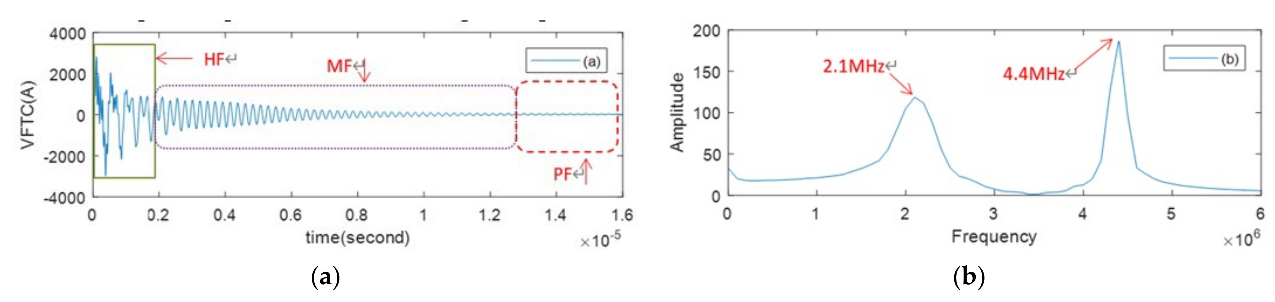
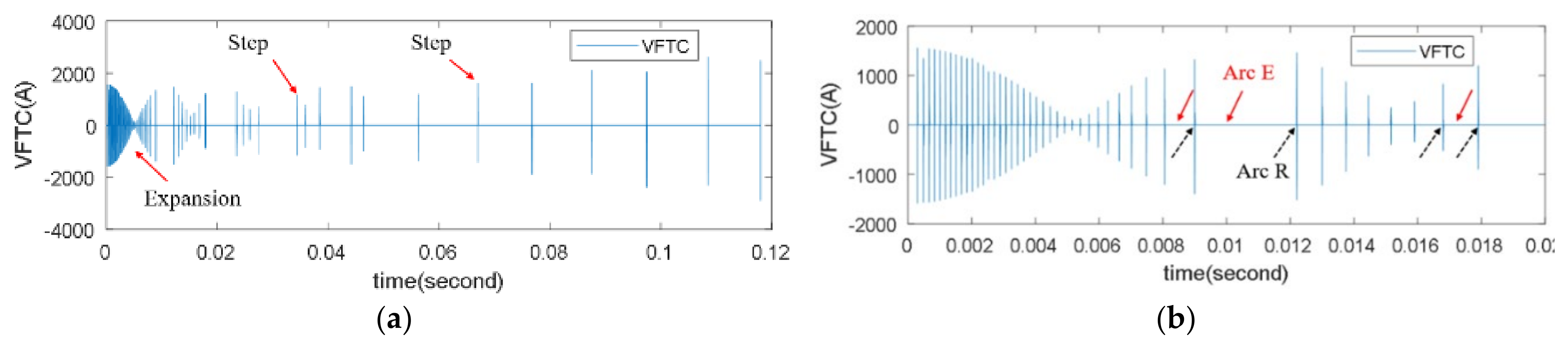
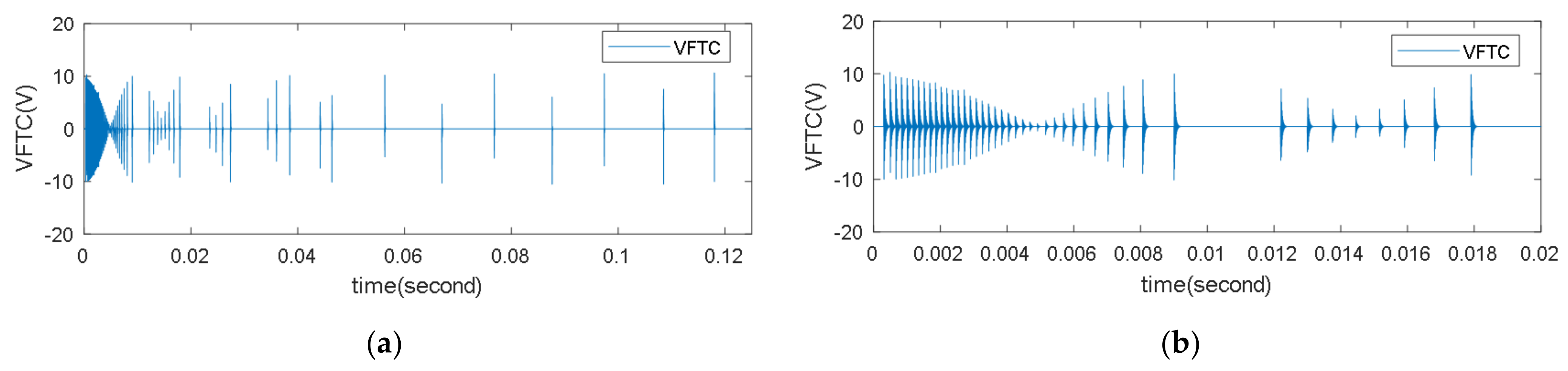
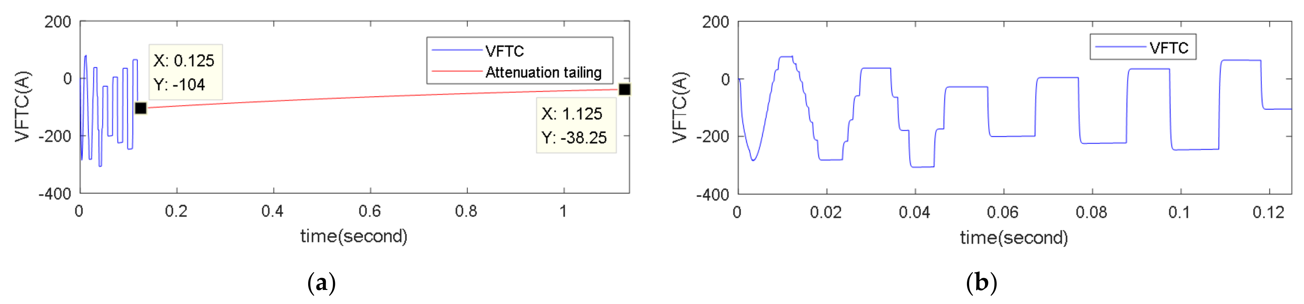
3.1. Subsection Simulation and Result Analysis of VFTC Signal Conduction in a Single Breakdown

Taking the simulation of closing the disconnector switch as an example, the most serious arc reignition is regarded as the condition before the switch operation, that is, the voltage on the power supply side is the positive peak value, and the residual charge voltage of the disconnected bus is the negative peak value of the power supply voltage (at the load of 22 nF). At this time, the power supply side voltage of the disconnector switch is 1.0 p.u. ( 110 / 3 × 2 = 89.8   kV ), and the load side voltage is −1.0 p.u. Table 5 demonstrates the signal transmission of the VFTC and subsequent links on the bus in detail.
The out waveforms of a single VFTC pulse are shown in Figure 6a, the transient current has oscillations at distinct frequencies, including high frequency (HF), medium frequency (MF) and the power frequency (PF). The magnitude of the VFTC is about 2.966 kA, and the frequency spectrum of the VFTC is shown in Figure 6b. Its dominant frequencies are 2.1 MHz and 4.4 MHz, and the highest one does not exceed 4.5 MHz. The VFTC only exists in the opening and closing process of the disconnector switch, and it appears to be a high-frequency oscillation attenuation wave. From the single VFTC breakdown waveform obtained by simulation, it is evident that the attenuation oscillation trend does not change after the high frequency current passes through zero, but lasts until the amplitude gradually tends to zero, as shown in Figure 6a. About 13 microseconds after the breakdown of the fracture of the disconnector switch, the instantaneous amplitude of the VFTC has been less than 10 A, which is almost submerged in the white noise, so it can be considered that the arc ignition process is over. This means that as the VFTC amplitude attenuation tends to 0 instead of reaching 0 (the arc burning time is around 13 us), the high-frequency arc will be extinguished, which is distinct from that the conventional high-voltage circuit breaker extinguishing the arc when the VFTC crosses zero.
When the steady-state rated input frequency is 50 Hz and the effective value is 2000 A, according to the parameters in Figure 3, the effective value of the Rogowski coil output’s secondary side is 0.15 V. The simulation results show that the disconnector will give origin to a large overcurrent VFTC (no TVS), and the maximum instantaneous value of high-frequency output induced by the Roche coil is 38 V, as shown in Figure 7, which far exceeds the 10 V maximum acceptable value at the sampling unit signal input port. This is a very severe challenge for the sampling unit itself, which will lead to the collapse of the corresponding integration circuit, resulting in extreme repercussions of irreversible failure.
In order to enhance the sampling unit’s anti-interference ability and reduce the effect of high-frequency voltage on the sampling unit, surge suppression, voltage clamping, and high-frequency interference signal filtering are carried out by adding the transient suppression diode TVS to the receiving signal end of the sampling unit and a low-pass filter after the integrator. When both periodic and the aperiodic components (DC component offset 100% of the short circuit current) exist at the same time [39], the formula for calculating the maximum voltage Umax of the sampling unit signal input in normal operation is as follows:
U max = U i n m × K a l f + U dc ( 100 % )
where Kalf is the overload multiple, and the value should not exceed 47. The result obtained by substituting the parameters into Equation (7) is:
U max = U i n m × K a l f + U dc ( 100 % ) = 0.15 × 2 × 23 . 6 + 5 = 10   V
If there is no DC component, the symmetrical AC signal can reach 47 times overload capacity. In order to restrain the damage to the circuit caused by the higher voltage, the TVS element is selected for clamping protection at the signal input end, and the reverse working voltage VRWM of TVS is selected as 10 V; The breakdown voltage is V(BR) = VRWM/0.85 = 11.76 V and the maximum clamping voltage is VC(MAX) = 1.30 × V(BR) = 15.3 V, taking 16 V. Therefore, the SMBJ10(C)A TVS can be selected to meet the requirements of the above parameters and the VFTC simulation waveform (added TVS) with the TVS is demonstrated in Figure 7. As can be seen, the amplitude has been limited to ±10 V and the presence or absence of the TVS has no effect on the system frequency f = 1/Δt = 1/14.63 μs = 68.35 kHZ which is consistent with the cut-off frequency of the Rogowski coil measured by the previous simulation.
The classic active integrator hardware, as shown in Figure 5, is called an ideal analog integrator when there is no feedback resistance Rf. At both ends of the integral capacitor C1 and C2, the integrator is connected in parallel with an M-level feedback resistor, primarily aimed at restraining the integral drift and making the integrator work stably for a long time. In Figure 5, we take T 1 = R f ( C 1 + C 2 ) = 1 , k 1 = R f R = 312 . 5 , and the integrator output is shown in Equation (9) [40]:
e 1 ( t ) = 1 R f C e t T 1 0 t e ( τ ) e τ T 1 d τ u c ( 0 + ) e t T 1
where e(τ) is the output of the Rogowski coil, taking τ as the independent variable of time t. T1 = RfC is the time constant of the integrator; uc(0+) is the initial voltage of the integral capacitor C at zero time, whose default value is 0.
As for the signal larger than 15.9 Hz processed by the active integrator selected in this paper, the higher the frequency of the signal is, the greater the amplitude gain. Besides, the change rate of gain with the increase of frequency is about −20 dB/dec attenuation and 90° phase shift. As shown in Figure 8, the active integrator output not only has adequate accuracy and stability, but also integrates the input signal, making the output stabilize at a fixed DC bias of 0.219 V after about Tlength = 160 us.
Calculated by Equation (6), the cut-off frequency of the first-order RC filter is 1 kHz, which effectively filters out the high-frequency signal of the active integrator output and finally stabilizes at t = 1.5 ms. At this time, the residual voltage of the integrator is 0.219 V (reduced to the primary current of 295.6 A), which is the residual charge voltage on the integral capacitors C1 and C2 and then the integrated capacitor discharges. The above process simulation is shown in Figure 9, and the specific process is explained in Figure 10.
In the RC circuit shown in Figure 10, the capacitors C1 and C2 have been charged before the switch S is switched off, and their voltage is U c 1 = U c 2 = e ( t ) . After the switch S is switched off, the energy stored in the capacitor C1 and C2 will be released in the form of thermal energy through the resistor. Taking the switch action time as the starting point (t = 0), right after the switch S is disconnected (t > 0), the equivalent circuit shown in Figure 10b derives Equation (10) according to the Kirchhoff Voltage Laws (KVL).
U R f U c = 0
where C = C1 + C2. Substituting U R f = i R f and i = C d U c d t into the above equation, we obtain:
R f C d U c d t + U c = 0
According to the initial conditions Uc(0+) = Uc(0) = e(t0+) = U0, the following results are obtained:
U R f = U c = U 0 e t R f C = U 0 e t τ
where τ is a time constant of RfC. It can be seen from the above expression that both URf and Uc attenuate according to the same exponential law, and their attenuation speed is determined by the time constant. According to the parameter selection in this paper, τ = RfC = 1 s, which means Uc(τ) = U0e−1 = 0.368U0 after 1 s (t = τ) and, as shown in Figure 9, the attenuation of the VFTC produced by a single breakdown complies with this law after passing through the integrator. The value of U0 depends on e(t), whose value range is [e(t)min~e(t)max].

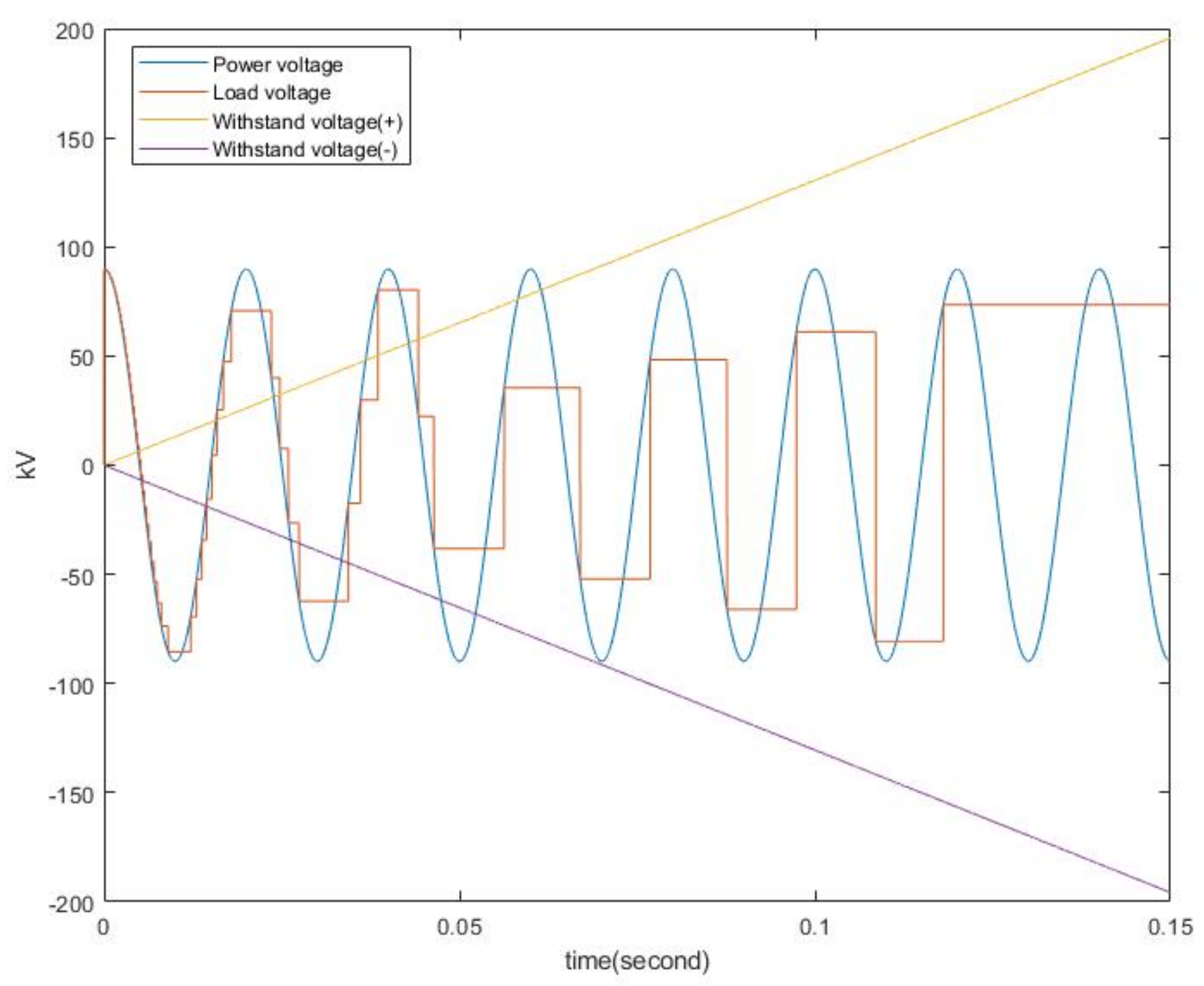
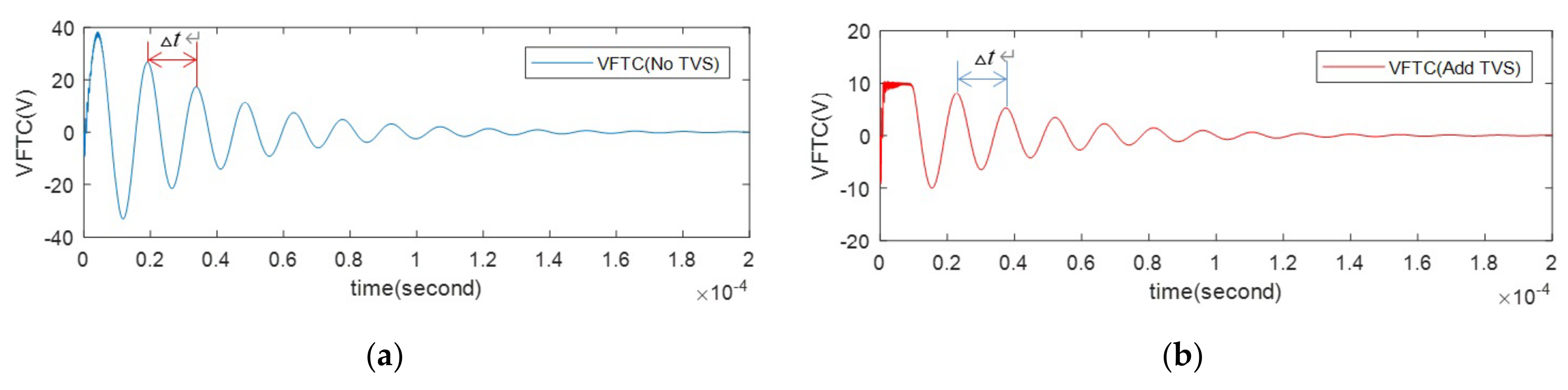
3.2. Simulation and Result Analysis of VFTC Signal Conduction in Multiple Breakdowns

The disconnector switch will break down many times during a complete switching process, and Table 6 gives the waveform characteristics of signals in different transmission links. As can be seen from Figure 11, the red arrows Arc E represent the arc extinction and the black arrows Arc R represent the arc reignition. There are 60 breakdowns occurring during the opening operation with a duration of 118 ms under the specified initial conditions. By analyzing the waveform of the VFTC, it can be found that the VFTC only exists in the single disconnector switch breakdown process, and it seems to be several pulses in the whole process of multiple breakdowns. Further, the VFTC waveform generates a transient process when each breakdown occurs, and the step size of the waveform change reaches the ns level. There is a relatively steady state stage with a ms-level step size between the end of this transient attenuation process and the formation of a new transient by the next breakdown. Besides, the breakdown numbers are relatively higher but the amplitude is smaller at the initial stage of opening, which will be less but larger at the later stage, while the closing process is the opposite, so it is not repeated here.
The VFTC waveform of the whole opening process obtained in Figure 11 is used as the input for the circuit shown in Figure 5, and the simulation step is 10 ns. In Figure 12, the Rogowski coil output waveform e(t) is given, which is also a repeated pulse waveform similar to the VFTC waveform input and also shows that the waveform has a 90° phase shift after the differential transformation of the initial VFTC signal. Therefore, under the use of the TVS, the maximum output amplitude is less than ±10 V, revealing that the TVS provides fast overvoltage protection for the circuit components.
After the Rogowski coil’s differential output waveform e(t) is restored by the integral of active integrator, the output waveform is e1(t), as shown in Figure 13, which can be seen as several attenuated shock waves. The attenuation waveform is relatively dense in the initial stage due to the small breakdown interval. Then, the attenuation waveform becomes loose with the increase of the breakdown interval. The expressions of e1(t) and e1n(t) are shown in Equations (13) and (14), respectively. After the attenuation is stable, the integral capacitor will carry out an exponential decay discharge with the time constant Δted = (tn+1 − tn) − Tlength, where the duration is (tn+1 − tn) = [Tmin, Tmax] = [0.17 ms, 11.1 ms], meaning that the residual charges on the integrating capacitors C1 and C2 have not been released yet, while the next breakdown comes again, repeated until the last breakdown discharge ends.
e 1 ( t ) = n = 1 60 e 1 n ( t )
where t = [t1, t60], meaning that the integral output consists of 60 single breakdown waveforms.
e 1 n ( t ) = 1 R f C e t t n T 1 t n t e n ( τ ) e τ T 1 d τ u c n ( 0 + ) e t t n T 1
where n = 1, 2, …, 60; t = [tn, tn+1], which indicates the duration of the attenuation waveform of a single breakdown until the next breakdown.
The integrated output waveform after filtering by the active filter is shown in Figure 14. As can be seen in Figure 13, the 1 kHz cut-off frequency filter can filter out the high-frequency instantaneous super value well, and the waveform returned to the primary current is relatively smooth after sampling at a frequency of 4 kHz (250 us sampling interval), with a maximum amplitude of 306.7 A, which is 10.8% of the peak value. The residual voltage on the integrator is discharged exponentially after the last breakdown with the time constant τ = T1 = 1 according to the law explained in Figure 10. After 1 s = (1.125 − 0.125), the residual voltage attenuates to 36.8% of the initial value (38.25/104), and the transition process ends after 5 s.
In addition to the conducted interference at the signal end analyzed above, the signal earth of the sampling unit is also vulnerable to interference during the disconnector switching. The main sources of high-frequency common-mode interference flowing through the PCB ground are the VFTC of the Rogowski coil, the distributed capacitance of power supply to ground, and the harmonics generated by a 50 MHz crystal oscillator of the digital circuit. These conducted interferences appear as high-frequency current Icm to the PCB ground, which flows through the ground, encounters the ground impedance ZGND and then generates a voltage drop (Icm × ZGND) that will form interference when superimposed on the normal signal Us. The ZGND in Figure 15 represents the ground impedance in the sampling unit PCB between the integral operational amplifier and the filter operational amplifier circuit [41]. In order to reduce the above interference, this paper adopts the Cy capacitor connected between the GND signal and the EARTH protective ground, mainly to provide the fastest low-impedance loop channel Icy for high-frequency signals to reduce the impact of high-frequency signals on the PCB circuit system.
The frequency of the crystal oscillator of the sampling unit selected in this paper is 50 MHz, and the voltage drop induced by the common mode interference flowing through the ground plane should not exceed 250 V and the leakage current should not exceed 0.25 mA. The Cy capacitance is calculated and selected according to these key parameters, and the formula for calculating the ground leakage current of the Cy capacitance is as follows:
I = U × 2 π f C y
where I is the leakage current, f is the test voltage frequency, U is the test voltage, and Cy is the Y capacitance between the GND signal and the EARTH protective ground connected to the PCB [42]. Substituting the parameters given in Figure 16 into Equation (15) we get the following result:
C y = I U × 2 π f = 0.21 × 10 3 250 × 2 × π × 60 = 2.229 × 10 9 F
Therefore, the capacitance of the Cy capacitor selected in this paper is 2200 pF (2.2 × 10⁻⁹ F), and the ceramic capacitor X1Y2: DE2E3KY222MA2BM01F meets the requirements of this paper, the characteristics of which are shown in Figure 16, where the insertion loss-frequency characteristics are shown in Figure 16a. As can be seen, the insertion loss is 34 dB near 30 MHz, and its amplitude attenuates to 2% of the original value. In order to protect the subsequent sampling circuit from being affected by high-frequency interference, the high-frequency common-mode signal is suppressed in the frequency band less than its resonant frequency.

4. Immunity Test of ECT When Disconnector Switching Small Capacitive Current

According to the test requirements of GB1985-2014 and the actual situation of the new generation intelligent substation project, the Test duty 3 for making and breaking bus-charging current is built at the China National High Voltage Apparatus Quality Supervision& Inspection Testing Center with reference to the circuit parameters given in Figure 1. The GIS ECT sensor developed in this paper is highly integrated to the GIS with the Rogowski coil as shown in Figure 17a. The sampling unit is installed on the GIS enclosure and has four types of ports: signal input, signal output, enclosure, and DC power input, as shown in Figure 17b. Figure 17c gives the installation position of the ECT and the physical drawing of the sampling unit developed in this paper is shown in Figure 18. The merging unit of the ECT is placed in the GIS control cabinet, and the fault recorder is connected to the ECT MU output to judge whether the ECT is malfunctioning during the operation of the disconnector switch. The complete GIS installed with the ECT is connected to the test circuit to simulate the process of disconnector switching the unloaded bus or capacitive small current load in the engineering site, resulting in severe transient interference, and the electromagnetic protection performance of the electronic transformer is evaluated under this condition. The standard requirements for the ECT to pass the test are [8]: (1) the ECT is not damaged; (2) there is no MU communication interruption, packet loss, and quality change; (3) abnormal MU output (the single point output exceeds 100% of the rated secondary output or 2 consecutive point outputs exceed 40% of the rated secondary output) is not permitted.
As shown in Figure 19, sixteen GIS disconnector switching capacitive load operation tests on the 110 kV ECT with a rated current of 2000 A are carried out. The amplitude and duration statistics of VFTC obtained from the sampling unit (Figure 18) are shown in Figure 20a,b, respectively.
When the test voltage is 110 / 3   63 . 5   kV , the maximum current peaks measured in the opening and closing process are 257.5 A and 66.656 A, reaching 9.1% and 2.36% of the rated current peak value 2000 × 2 A , respectively. The duration of the opening is related to the residual charge of the capacitive load and the instantaneous voltage of the power supply at the first breakdown. The test results fully meet the requirements of the above introduced criteria. The typical VFTC output of the merging unit during the opening operation of the disconnector switch is shown in Figure 21c and its expansion Figure 21d, and the trailing attenuation of current is caused by the first-order discharge circuit RfC formed by the sampling unit’s integral feedback resistance and capacitance. In the whole process of the test, the ECT did not exceed the three assessment values required in the above-mentioned standards.
It can be seen from Figure 21 that there are small burrs in the output signal waveform, which are mainly induced by the input offset voltage of the operational amplifier AD8610B. Although the DC negative feedback loop is designed in an active integrator to suppress the accumulated DC component, it cannot be eliminated completely, so the zero-drift algorithm is needed for further processing in the merging unit’s software program. The primary current i1(t) is obtained by reducing e1(t), and its time domain expression can be expressed as follows:
i 1 ( t ) = R C M e 1 ( t ) = 1 M e t R f C 0 t e ( τ ) e τ R f C d τ + 1 M e t R f C 0 t V o s ( τ ) e τ R f C d τ + R C M V c ( 0 + ) e t R f C
where i o s ( t ) = 1 M e t R f C 0 t V o s ( τ ) e τ R f C d τ is caused by the input offset voltage of the operational amplifier [39]. In the simulation, there is no offset voltage in the ideal operational amplifier AD8610B, so the waveform can be quite smooth.

5. Conclusions

This paper simulates and analyzes the VFTC characteristics and the interference characteristics transmitted step by step through the Rogowski coil and the sampling unit in the process of the test duty 3 of bus-charging currents switching by a 110 kV GIS disconnector, and the switching capacitive small current of the disconnector switch is verified experimentally. The results of this paper can be summarized as follows:
  • During the switching process of the disconnector, the VFTC produced with the VFTO is the root of conducting interference generated by the GIS ECT. The cut-off frequency of the Rogowski coil (≥1 kHz) is reduced as much as possible on the premise of the ECT installation size to greatly attenuate the high-voltage and high-frequency signal.
  • In view of the characteristics of the response simulation waveform of each node in single and multiple breakdowns, the TVS selected in this paper can effectively intercept signals ≥10 V; the designed 1 kHz filter can effectively filter out high-frequency signals (≤68 kHz) and the selected 2200 pF capacitor Cy provides the fastest low-impedance release circuit for the PCB ground interference (≤60 MHz). The above design ensures that the output interference of the ECT does not exceed 40% of the rated current during the opening and closing process of the disconnector switch, which meets the requirements of the evaluation standard.
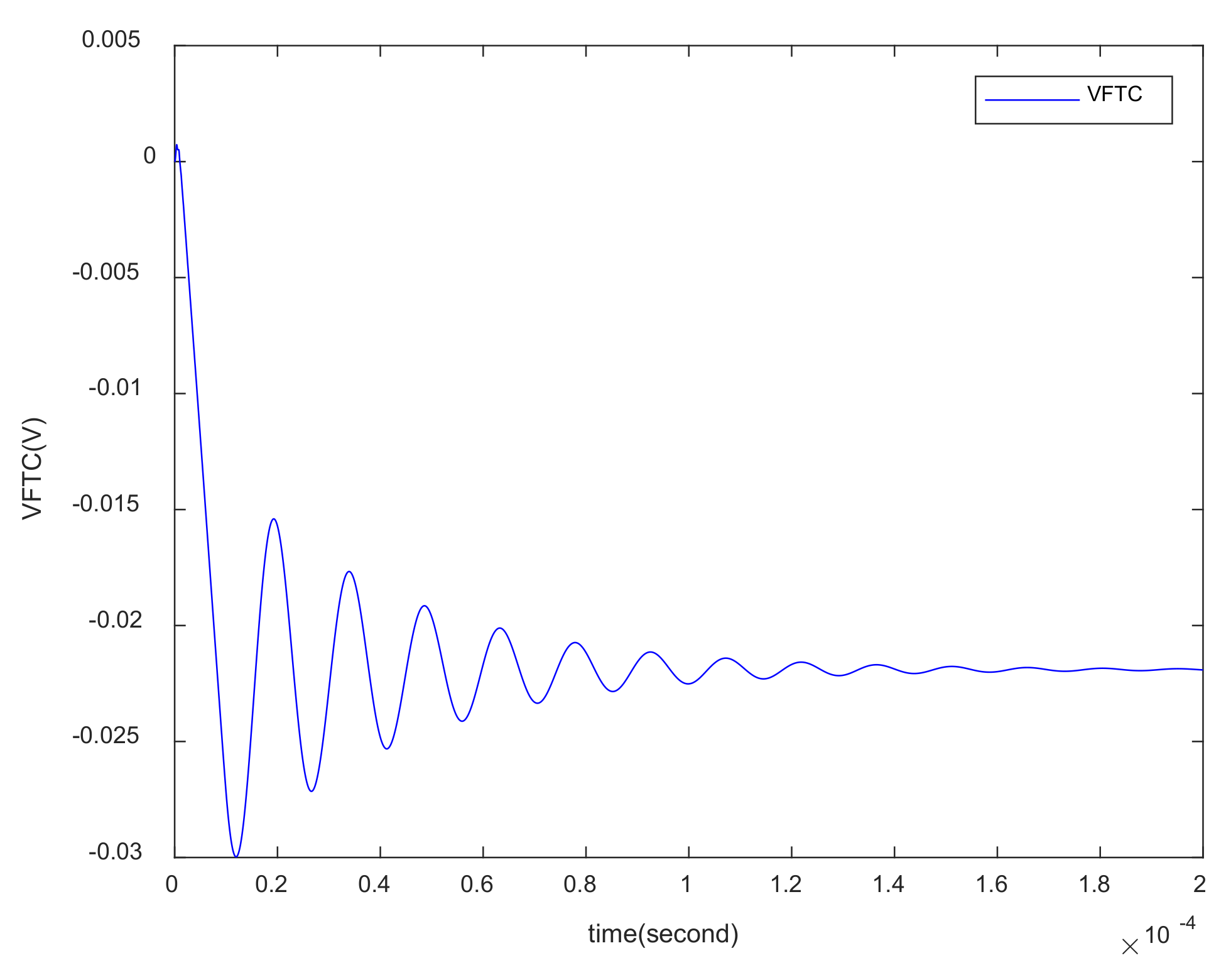
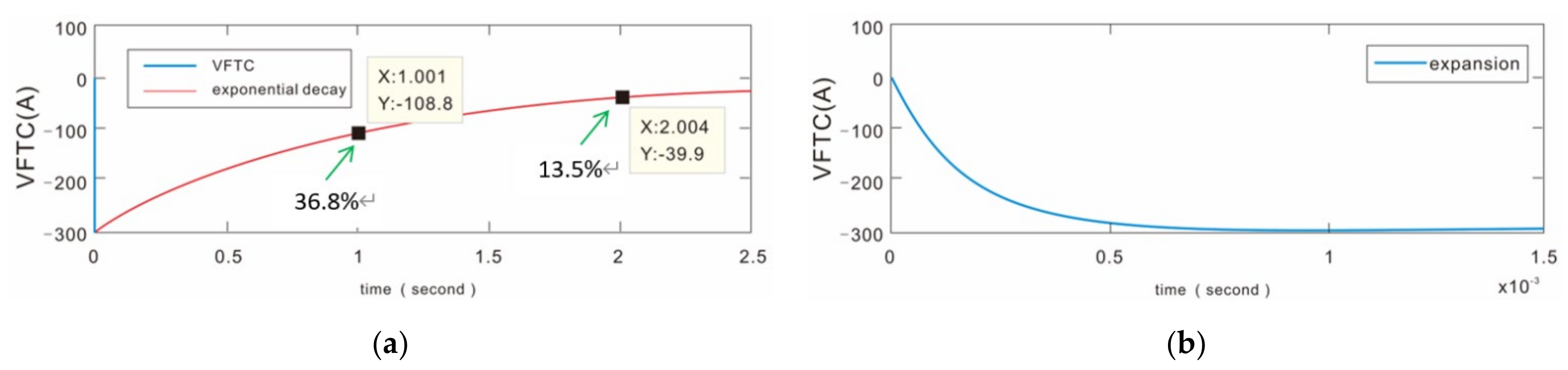
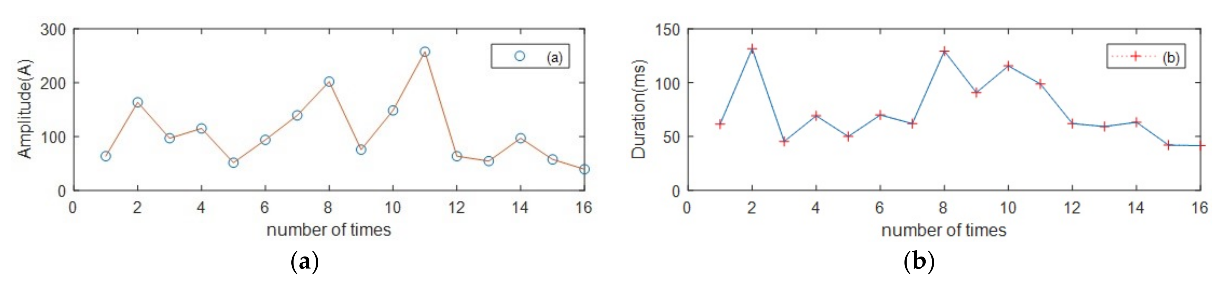
  • The experimental test was carried out to measure the output value of the merging unit during the switching process of the disconnector. As derived from the measurement, the residual charge of the integrated capacitor discharges exponentially with the time constant τ = 1 s after arc extinguishing, and its characteristics are consistent with the simulated waveform, which demonstrates the equivalence of the simulation model built in this paper. In the design of the conducted interference of the 110 kV and higher voltage level ECT, the simulation has a certain universality and popularizing value.

Author Contributions

Conceptualization, S.B., X.W. and M.R.; formal analysis, S.B., X.W. and M.R.; investigation, S.B.; methodology, L.Z. and C.W.; software, S.B.; validation, Y.L.; writing—original draft, S.B. and F.Y.; writing—review and editing, F.Y. All authors have read and agreed to the published version of the manuscript.

Funding

This research received no external funding.

Institutional Review Board Statement

Not applicable.

Informed Consent Statement

Not applicable.

Data Availability Statement

Not applicable.

Conflicts of Interest

The authors declare no conflict of interest.

References

  1. Smeets, R.R.; Van Der Linden, W.; Achterkamp, M.; Damstra, G.; De Meulemeester, E. Disconnector switching in GIS: Three-phase testing and phenomena. IEEE Trans. Power Deliv. 2000, 15, 122–127. [Google Scholar] [CrossRef]
  2. Haznadar, Z.; Carsimamovic, S.; Mahmutcehajic, R. More accurate modeling of gas insulated substation components in digital simulations of very fast electromagnetic transients. In Proceedings of the Power Industry Computer Application Conference, Sydney, Australia, 7–10 May 1991. [Google Scholar]
  3. Heimbach, M. VFT studies on current and voltage transformers in GIS by means of an iterative pole-zero-removal method for simulating the transfer function. In Proceedings of the Ninth International Symposium on High Voltage Engineering, Graz, Austria, 28 August–1 September 1995; pp. 6751–6752. [Google Scholar]
  4. Heimbach, M.; Grcev, L. Grounding system analysis in transients programs applying electromagnetic field approach. IEEE Trans. Power Deliv. 1997, 12, 186–193. [Google Scholar] [CrossRef]
  5. Limin, F.; Xiaobo, W.; Lianzi, W. Study on the impact of VFTO electromagnetic interference on electronic transformers in 500 kV GIS substation. Trans. China Electrotech. Soc. 2016, 31, 85–90. [Google Scholar]
  6. Wiggins, C.; Thomas, D.; Nickel, F.; Salas, T.; Wright, S. Transient electromagnetic interference in substations. IEEE Trans. Power Deliv. 1994, 9, 1869–1884. [Google Scholar] [CrossRef]
  7. Liu, B.; Ye, G.; Guo, K.; Tong, Y.; Hu, B.; Wan, G. Quality test and problem analysis of electronic transformer. Gaodianya Jishu High Volt. Eng. 2012, 38, 2972–2980. [Google Scholar]
  8. Li, Z.; Shen, J.; Li, H.; Wu, L.; Zhang, T.; Xu, Y. Research on Arc Model of Disconnector for Conduction Interference of Electronic Transformer. In Proceedings of the 2019 4th International Conference on Intelligent Green Building and Smart Grid (IGBSG), Yichang, China, 6–9 September 2019; pp. 443–447. [Google Scholar]
  9. Lin, C.; Zhu, Y.; Chen, F.; Yu, H.; Zhang, C.; Liu, X.; Wang, W.; Wang, Y.; Deng, X.; Gao, J.; et al. Research on Electromagnetic Interference of Smart Device Acquisition Unit under GIS Disconnector Operation. IOP Conf. Ser. Mater. Sci. Eng. 2018, 452, 042190. [Google Scholar] [CrossRef]
  10. Zhenhua, L.; Weizhong, H.; Suhong, Y. Conductive interference analysis and anti-interference methods of electronic transformers in disconnector switching test. High Volt. Eng. 2016, 42, 233–240. [Google Scholar]
  11. Zhang, J.; Zhao, J.; Xie, P. Simulation and analysis of electromagnetic properties at the secondary port of electronic current transformers under very fast transient overvoltage. Trans. China Electrotech. Soc. 2015, 30, 88–94. [Google Scholar]
  12. Bai, S.; Zeng, L.; Rong, M.; Li, Y.; Chen, K.; Zhang, Y. Interference Analysis and Protection of Electronic Current Transformer Caused by Disconnect Switch Operation in GIS. High Volt. Appar. 2016, 52, 54–62. [Google Scholar] [CrossRef]
  13. Bai, S.; Zeng, L.; Li, Y.; Zhang, C.; Jia, L. Anti-interference Measures Research and Protection of Electronic Transformer Applied in Engineering. High Volt. Appar. 2016, 52, 187–193. [Google Scholar] [CrossRef]
  14. Rao, M.; Thomas, M.; Singh, B. Frequency Characteristics of Very Fast Transient Currents in a 245-kV GIS. IEEE Trans. Power Deliv. 2005, 20, 2450–2457. [Google Scholar] [CrossRef]
  15. Wei, M.; Wu, X.; Yu, G.; Tian, Y.; Wu, S. Study on Transient Characteristics of VFTC in 1 100 kV GIS Substation. Electr. Power 2016, 49, 1–8. [Google Scholar] [CrossRef]
  16. Chai, Y.Y.; Wouters, P.A.A.F.; Van Hoppe, R.T.W.J.; Smeets, R.P.P.; Peelo, D.F. Capacitive Current Interruption with Air-Break High Voltage Disconnectors. IEEE Trans. Power Deliv. 2010, 25, 762–769. [Google Scholar] [CrossRef]
  17. Chai, Y.; Wouters, P.A.A.F.; Smeets, R.P.P. Capacitive Current Interruption by HV Air-Break Disconnectors with High-Velocity Opening Auxiliary Contacts. IEEE Trans. Power Deliv. 2011, 26, 2668–2675. [Google Scholar] [CrossRef]
  18. Narimatsu, S.; Yamaguchi, K.; Nakano, S.; Maruyama, S. Interrupting Performance of Capacitive Current by Disconnecting Switch for Gas Insulated Switchgear. IEEE Trans. Power Appar. Syst. 1981, PAS-100, 2726–2732. [Google Scholar] [CrossRef]
  19. Bojic, P. Bus charging current switching in GIS by disconnector. IEEE Porto Power Tech Proc. 2002, 3, 6. [Google Scholar] [CrossRef]
  20. Duan, S.; Zhan, H.; Li, C.; Zhao, L.; Yao, L. Measurement and modelling of Very Fast Transient Current in 220 kV GIS. Vacuum 2015, 120, 32–36. [Google Scholar] [CrossRef]
  21. Liu, B.; Ye, G.; Tong, Y. Influence of disconnector in gas insulated switchgear switching on/off on electromagnetic compatibility of electronic transformer. High Volt. Eng. 2018, 44, 1204–1210. [Google Scholar]
  22. IEC 62271-102-2001. High-Voltage Switchgear and Controlgear—Part 102: Alternating Current Disconnectors and Earthing Switches. Available online: https://sales.sfs.fi/fi/index/tuotteet/IEC/IEC/ID9988/6/333413.html.stx (accessed on 23 July 2020).
  23. IEC. Instrument Transformers Part 8 Electronic Current Transformers; IEC: Geneva, Switzerland, 2002. [Google Scholar]
  24. GB/T 20840. 8-2007. Instrument Transformers-Part 8: Electronic Current Transformers. Available online: https://www.chinesestandard.net/PDF/English.aspx/GBT20840.8-2007 (accessed on 23 July 2020).
  25. Duan, S.; Zhao, L.; Li, Z.; Zhan, H.; Li, C. Experimental and simulation study on statistical characteristics of VFTO and VFTC in GIS. Power Syst. Technol. 2015, 39, 3634–3640. [Google Scholar]
  26. Kumar, V.; Thomas, J.; Naidu, M. Influence of switching conditions on the VFTO magnitudes in a GIS. IEEE Trans. Power Deliv. 2001, 16, 539–544. [Google Scholar] [CrossRef]
  27. Carsimamovic, S.; Bajramović, Z.; Ljevak, M.; Veledar, M. Very fast electromagnetic transients in air insulated substations and gas insulated substations due to disconnector switching. In Proceedings of the 2005 International Symposium on Electromagnetic Compatibility, Chicago, IL, USA, 8–12 August 2005. [Google Scholar]
  28. Tavakoli, A.; Gholami, A.; Parizad, A.; Soheilipour, H.; Nouri, H. Effective factors on the very fast transient currents and voltage in the GIS. In Proceedings of the 2009 Transmission & Distribution Conference & Exposition: Asia and Pacific, Seoul, Korea, 26–30 October 2009; pp. 1–6. [Google Scholar]
  29. Reddy, P.R.; Amarnath, J. Simulation of Mitigation Methods for VFTO’S And VFTC’S in Gas Insulated Substations. In Proceedings of the 15th IEEE conference on Advanced Computing Technologies (ICACT), New Boyanapalli, India, 21–22 September 2013. [Google Scholar]
  30. Miri, A.; Stojkovic, Z. Transient electromagnetic phenomena in the secondary circuits of voltage and current transformers in GIS (measurements and calculations). IEEE Trans. Power Deliv. 2001, 16, 571–575. [Google Scholar] [CrossRef]
  31. Huamao, Z.; Chengnan, Z.; Shaofeng, D. Measuring of very fast transient over-voltage and very fast transient current generated by disconnector in gas insulated switchgear switching on/off short buses with no load. High Volt. Eng. 2013, 39, 1317–1323. [Google Scholar]
  32. Yinbiao, S.; Bin, H.; Ji-Ming, L.; Weijiang, C.; Liangeng, B.; Zutao, X.; Guoqiang, C. Influence of the Switching Speed of the Disconnector on Very Fast Transient Overvoltage. IEEE Trans. Power Deliv. 2013, 28, 2080–2084. [Google Scholar] [CrossRef]
  33. Du, W.; Li, Y.; Liu, J. A new VFTO whole process simulation method based on time domain finite element. Proc. CSEE 2014, 34, 3004–3012. [Google Scholar]
  34. Filho, J.G.R.; Teixeira, J.A.; Sans, M.R.; Martinez, M.L.B., Jr.; Teixeira, J.A. Very fast transient overvoltage waveshapes in a 500-kV gas insulated switchgear setup. IEEE Electr. Insul. Mag. 2016, 32, 17–23. [Google Scholar] [CrossRef]
  35. Zhang, Y. Simulation Analysis and Design of Rogowski Coil Current Transformer; Haerbin Institute of Technology: Haerbin, China, 2006; pp. 56–58. [Google Scholar]
  36. Jiao, C.; Zhang, J.; Zhao, Z.; Zhang, Z.; Fan, Y. Research on Small Square PCB Rogowski Coil Measuring Transient Current in the Power Electronics Devices. Sensors 2019, 19, 4176. [Google Scholar] [CrossRef] [Green Version]
  37. Xie, B.; Yin, X.-G.; Zhang, Z.; Li, W. Technology in designing integrator of electronic current transducer based on Rogowski coil. Relay 2007, 35, 45–50. [Google Scholar]
  38. Wang, J.; Si, D.; Tian, T.; Ren, R. Design and Experimental Study of a Current Transformer with a Stacked PCB Based on B-Dot. Sensors 2017, 17, 820. [Google Scholar] [CrossRef] [PubMed] [Green Version]
  39. Ma, Y.; Xia, Y.; Song, B.; Shen, Z.; Wang, H. Quantitative Analysis of Time Constant of Analog Integrator Used for Air-core Coil. Shandong Electr. Power 2019, 46, 21–25. [Google Scholar] [CrossRef]
  40. ZHENG, Y. Analysis on abnormal magnetizing inrush current output from electronic current transformer when no-load transformer operates. Autom. Electr. Power Syst. 2017, 41, 188–193. [Google Scholar]
  41. Zheng, J. Electromagnetic Compatibility (EMC) Design and Test Case Analysis; Wiley: Hoboken, NJ, USA, 2019. [Google Scholar]
  42. He, J.; Li, X. Interaction of X-capacitor and Y-capacitor Between Electrical Safety and EMC Performance. Safety EMC 2019, 31–33, 38. [Google Scholar]
Figure 1. Test duty 3 of switching of bus-charging currents circuit.
Electronics 10 00957 g001
Figure 2. Model of the very fast transient current (VFTC) simulation circuit.
Electronics 10 00957 g002
Figure 3. Simulation flow chart of VFTC.
Electronics 10 00957 g003
Figure 4. Power supply voltage, load side residual voltage, and breakdown voltage during the opening process of the disconnector switch.
Electronics 10 00957 g004
Figure 5. Simulation circuit of the Rogowski coil and integral filter.
Electronics 10 00957 g005
Figure 6. VFTC waveforms at GIS bus (ECT) for disconnector switching (DS) operation (S. No1): (a) single current waveform; (b) frequency spectra of the VFTC.
Electronics 10 00957 g006
Figure 7. VFTC waveforms at the secondary port of the Rogowski coil (S. No2). (a) No TVS; (b) added TVS.
Electronics 10 00957 g007
Figure 8. VFTC waveforms at the output of active integrator (S. No3).
Electronics 10 00957 g008
Figure 9. The wave shapes of VFTC Output of filter (AD sampling) and its expansion (S. No4). (a) VFTC waveforms; (b) the expansion of VFTC waveforms.
Electronics 10 00957 g009
Figure 10. The first-order discharge circuit composed of feedback resistors and integral capacitors: (a) zero input response of RC Circuit; (b) first-order RC discharge equivalent circuit.
Electronics 10 00957 g010
Figure 11. VFTC waveforms at GIS bus (ECT) and its expansion (S. No1): (a) VFTC waveforms; (b) the expansion of VFTC waveforms.
Electronics 10 00957 g011
Figure 12. VFTC waveforms in the whole process at the secondary port of the Rogowski coil (S. No2). (a) VFTC waveforms; (b) the expansion of VFTC waveforms.
Electronics 10 00957 g012
Figure 13. VFTC waveforms in the whole process at the output of active integrator (S. No3). (a) VFTC waveforms; (b) the expansion of VFTC waveforms.
Electronics 10 00957 g013
Figure 14. VFTC waveforms in the whole process at the output of filter (AD sampling) (S. No4). (a) VFTC waveforms; (b) the expansion of VFTC waveforms.
Electronics 10 00957 g014
Figure 15. Voltage drops caused by common mode interference current flowing through ground impedance.
Electronics 10 00957 g015
Figure 16. 2200 pf Cy capacitance characteristics: (a) insertion loss-frequency characteristics; (b) impedance frequency characteristic.
Electronics 10 00957 g016
Figure 17. The GIS electronic current transformer developed in this paper: (a) Rogowski coil; (b) 110 kV ECT (no included merging unit); (c) ECT installed on 110 kV GIS.
Electronics 10 00957 g017
Figure 18. The sampling unit developed in this paper.
Electronics 10 00957 g018
Figure 19. Experimental setup of the ECT (Test duty 3).
Electronics 10 00957 g019
Figure 20. Statistics of key parameters of VFTC opening: (a) maximum amplitude of VFTC; (b) VFTC duration.
Electronics 10 00957 g020
Figure 21. Typical wave shapes of iPF, Ul, VFTC and its expansion. (a) iPF waveforms; (b) Ul waveforms; (c) VFTC waveforms; (d) the expansion of VFTC waveforms.
Electronics 10 00957 g021
Table 1. Main parameters of power frequency voltage measurement system.
ParametersNotesValue
TTPF transformer (50 Hz)400/1600 (kV/kVA)
RpProtection resistance5 kΩ
C01H.V arm capacitance500 pF
C02L.V arm capacitance3 uF
C03H.V arm capacitance400 pF
C04L.V arm capacitance0.4 uF
ClLoad capacitance22 nF
CTCurrent transformer
DSDisconnector switch
VVoltmeter
CR0Data Acquisition System
ECTElectronic current transformer5 TPE
Table 2. Equivalent circuits and value of circuit components.
ComponentNotes
Transformer (Power)L = 20 mH, C = 1000 pF
High voltage lineZ = 350–400 Ω
Gas-to-air BushingTransmission line of surge impedance 250 Ω and capacitance of 20 pF towards ground on either end of the contacts.
SpacersCapacitance of 20 pF towards ground.
GIS bus barZ = 40–90 Ω, v = 270 m/us
Circuit breaker (CB)Transmission line of surge impedance 23.4 Ω and capacitance of 20 pF towards ground on either end of the contacts. In open condition, a capacitance of 40 pF between contacts.
Earthing switch (ES)Equivalent circuit of the Rogowski coil
ECTCurrent transformer
CVT1C01 = 500 pF, C02 = 3 uF
CVT2C03 = 400 pF, C04 = 0.4 uF
Disconnector switch (DS) R = R e t / τ 1 i + R e t / τ 2 c
Load capacitance22 nF
Table 3. Technical parameters of the 110 kV gas-insulated switchgear (GIS) disconnector.
ParametersNotes
Type of isolation switchSlow, electric
closing (mm)97.5
L, Fracture distance (mm)55
opening time (ms)685
vopen, Opening speed (m/s)0.062
closing time (ms)792
vclose, closing speed (m/s)0.069
Table 4. Main parameters of the Rogowski coil sensor.
StyleParametersValue
Structurerb (outer radius)/m0.11
ra (internal radius)/m0.095
H(height)/m0.015
B(width)/m0.015
N/turns543
ElectromagnetismM/uH0.2387
L0/mH0.13
C0/uF0.0418
R07.135
Rs15 k
Table 5. Transient VFTC at different electronic current transformer (ECT) component points (single).
S. NoPositionAmplitude UnitWaveform
1GIS bus (ECT)AFigure 6
2the secondary port of Rogowski coilVFigure 7
3Output of active integratorVFigure 8
4(AD sampling)AFigure 9
Table 6. Transient VFTC at different ECT component points (the whole process).
S. NoPositionAmplitude UnitWaveform
1GIS bus (ECT)AFigure 11
2the secondary port of Rogowski coilVFigure 12
3Output of active integratorVFigure 13
4(AD sampling)AFigure 14
Publisher’s Note: MDPI stays neutral with regard to jurisdictional claims in published maps and institutional affiliations.

