
A 6-Locking Cycles All-Digital Duty Cycle Corrector with Synchronous Input Clock


Abstract
1. Introduction
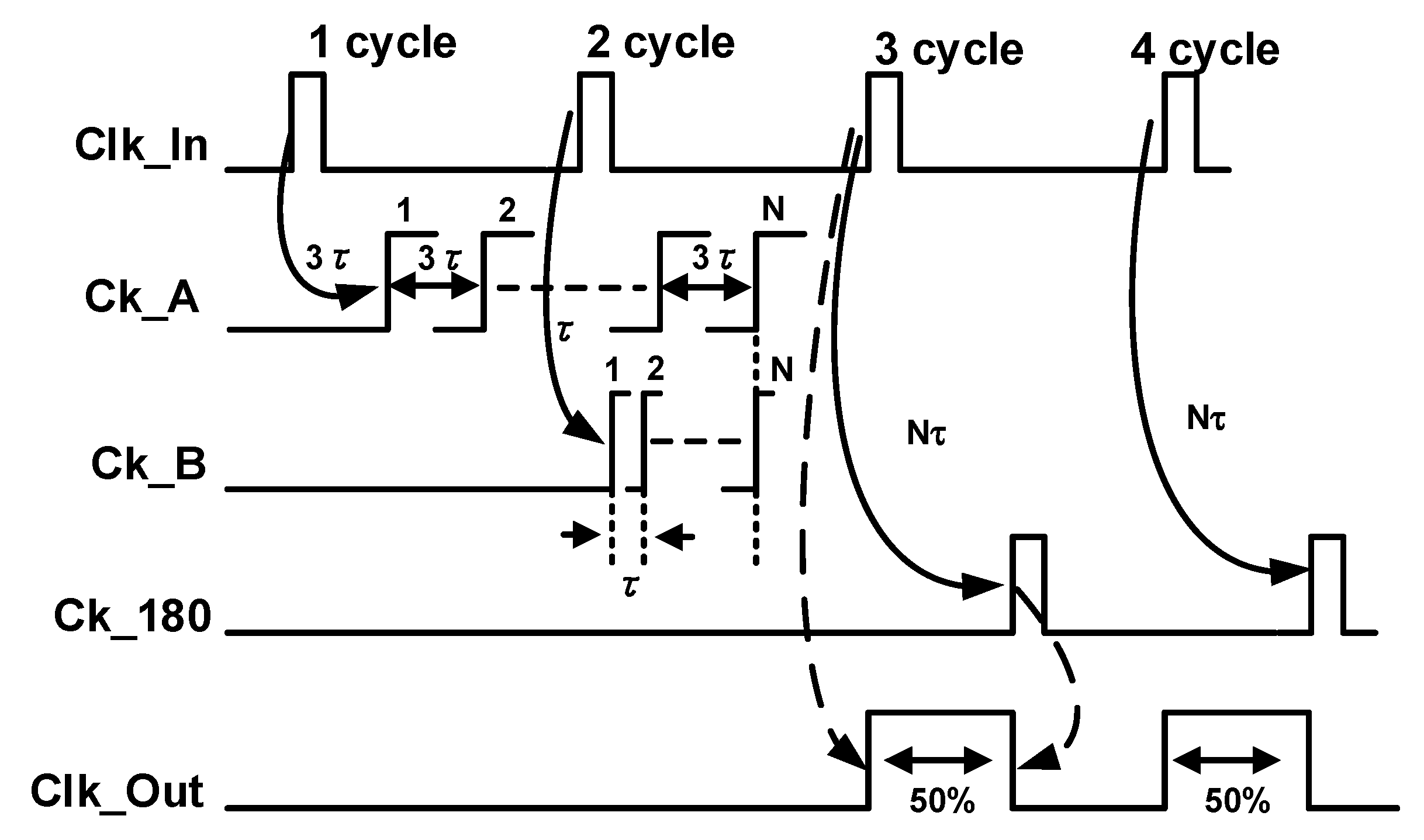
2. State-of-the-Art
3. Circuit Architecture Design
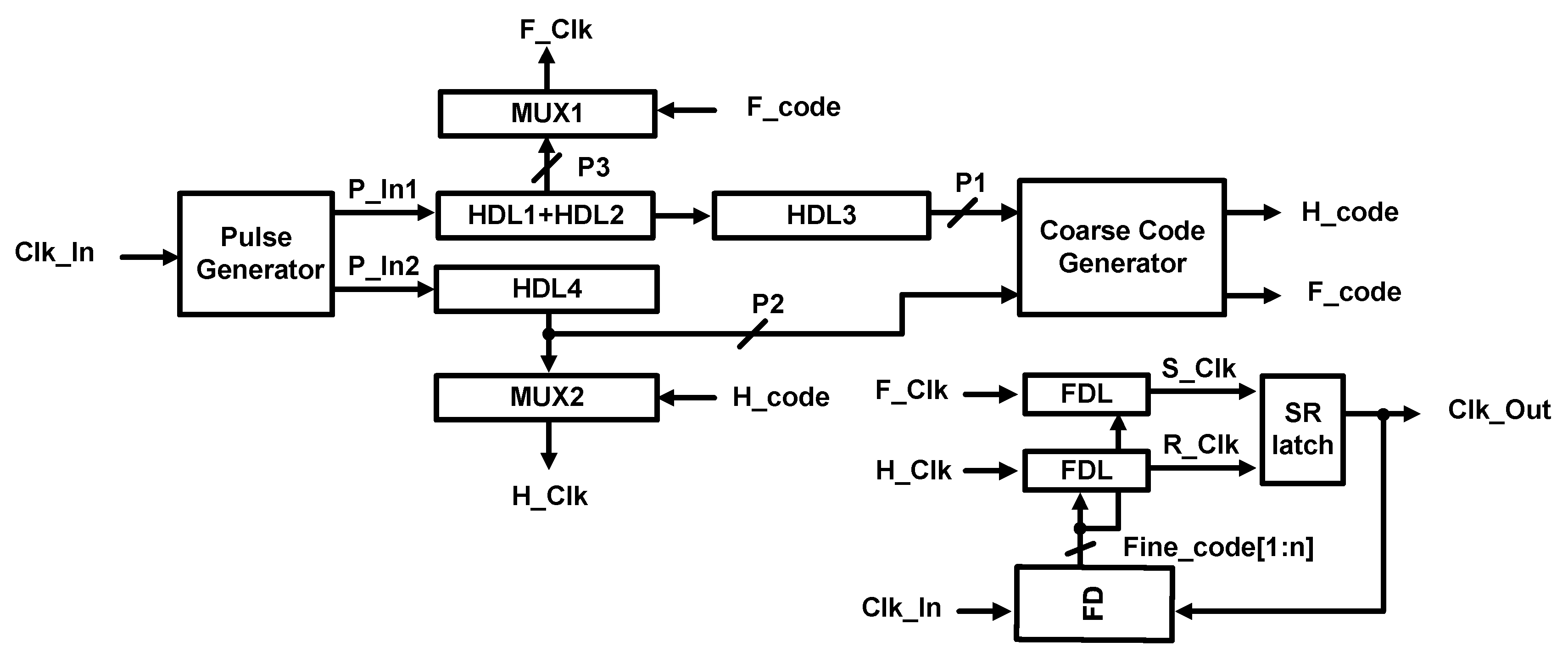
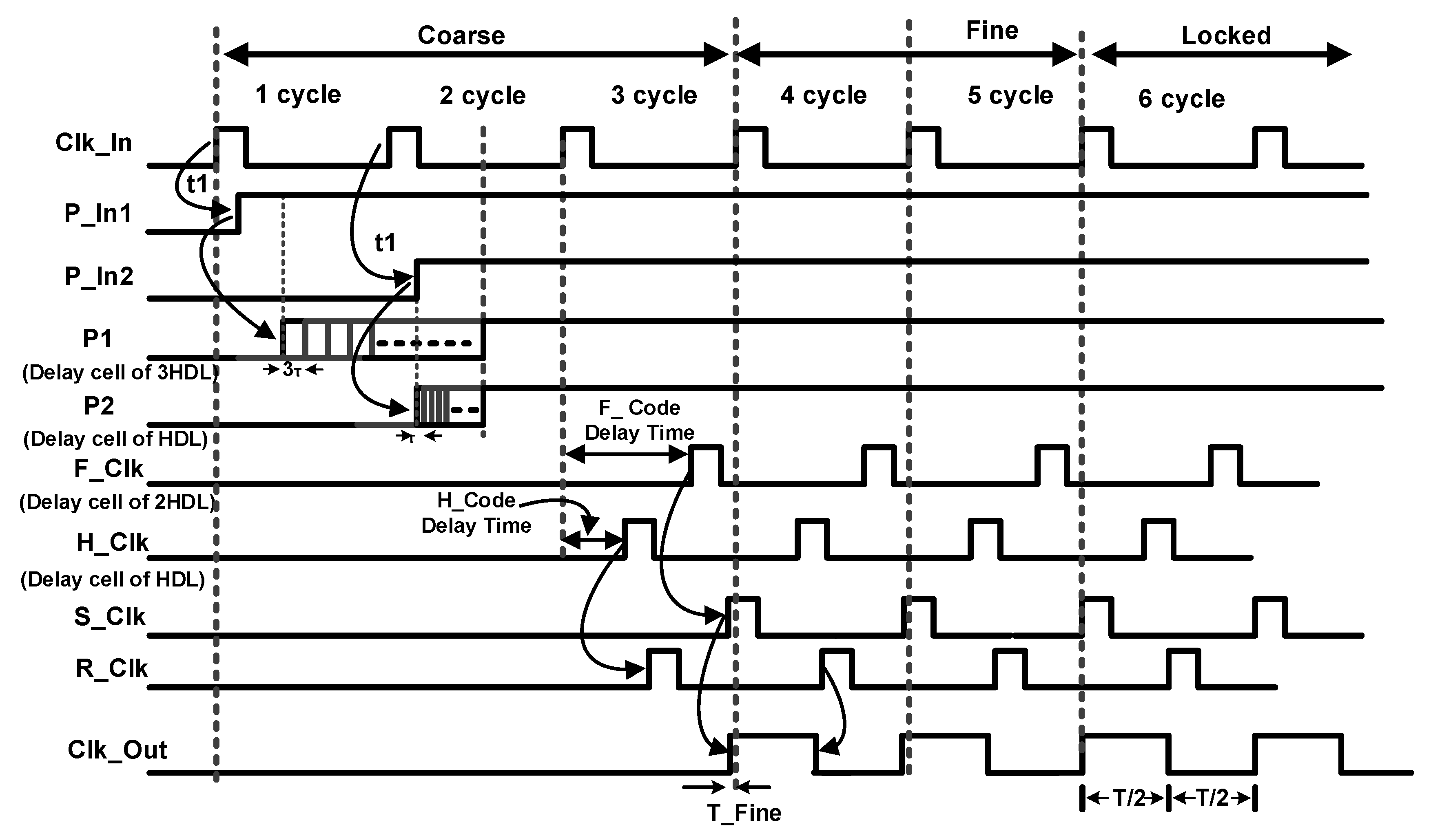
4. Circuit Architecture
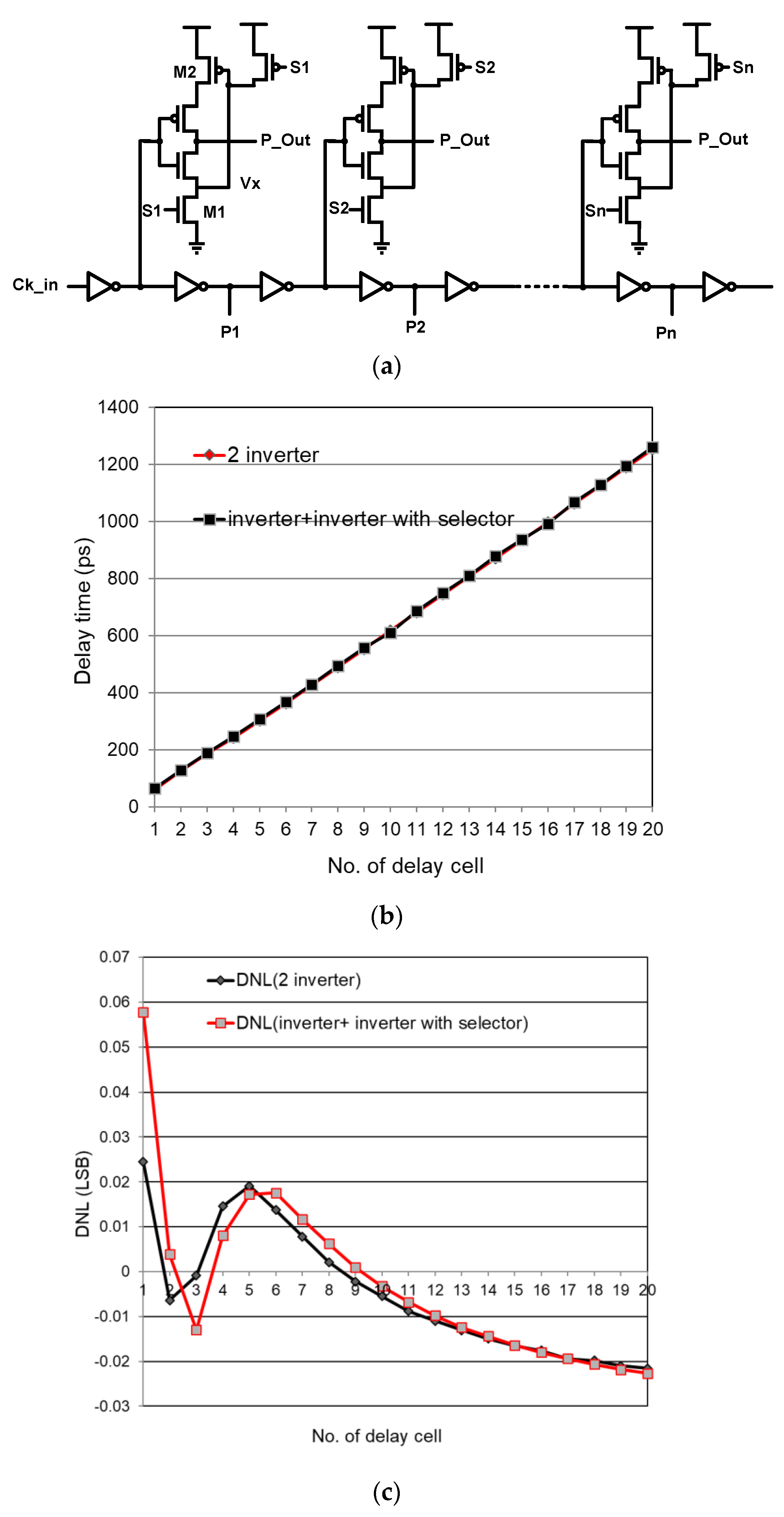
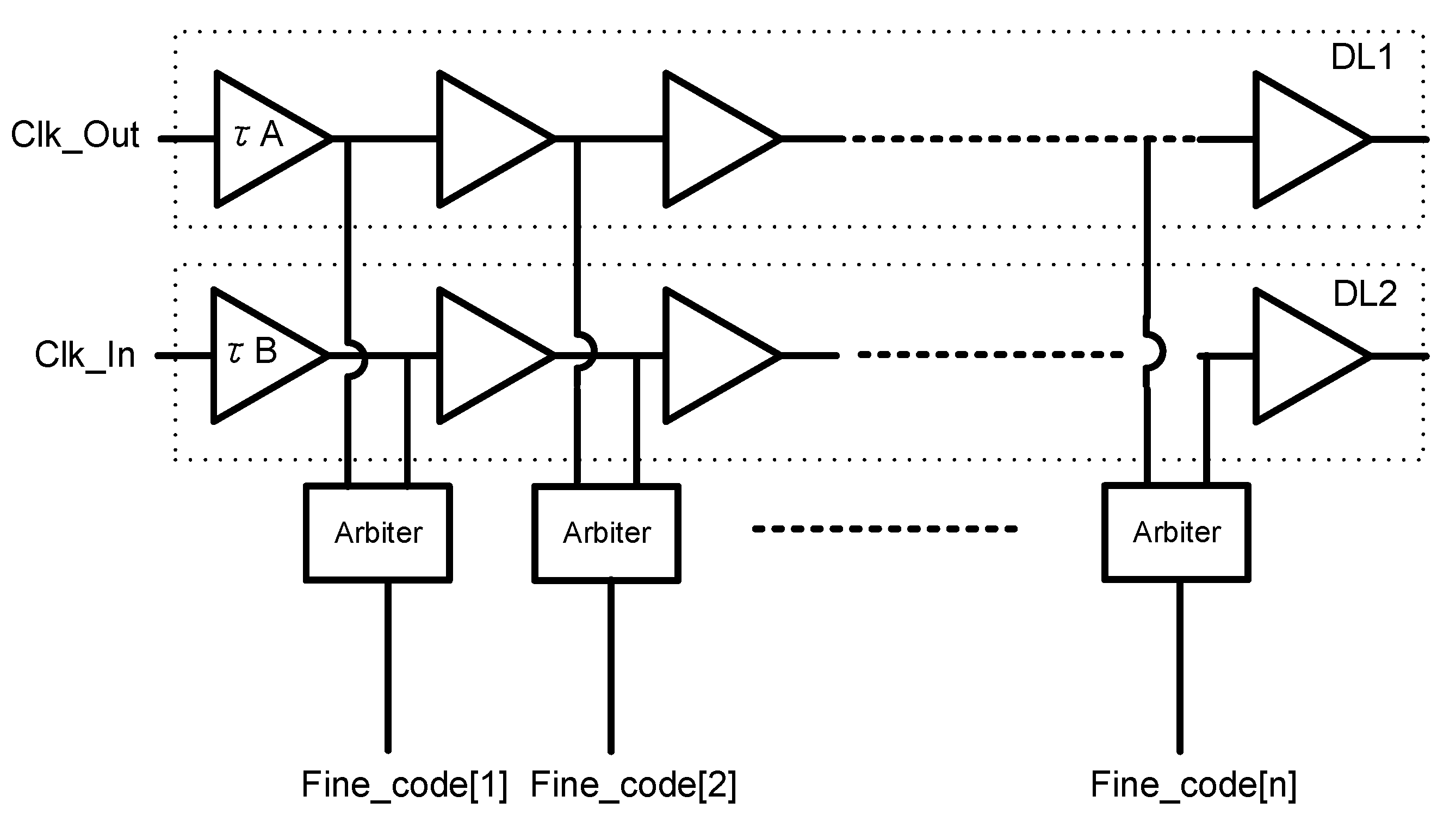
4.1. Half-Delay Line
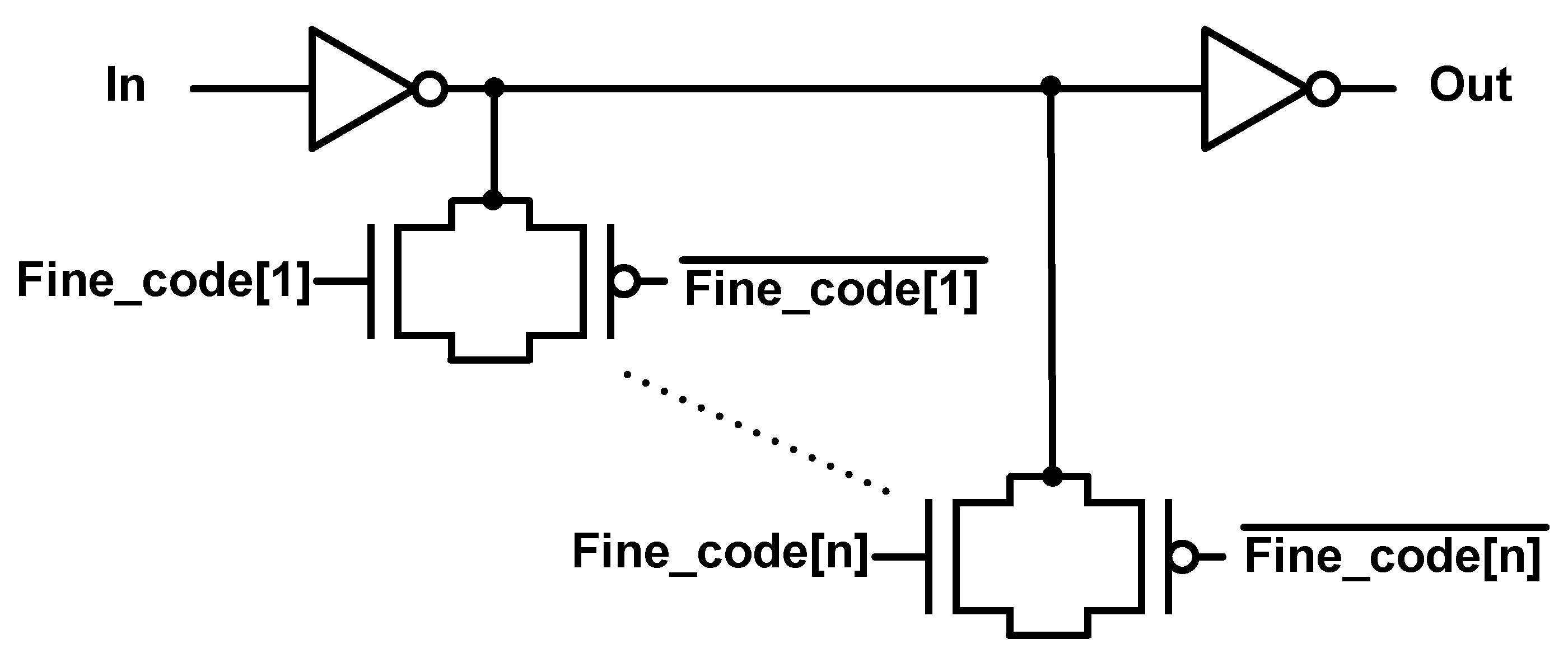
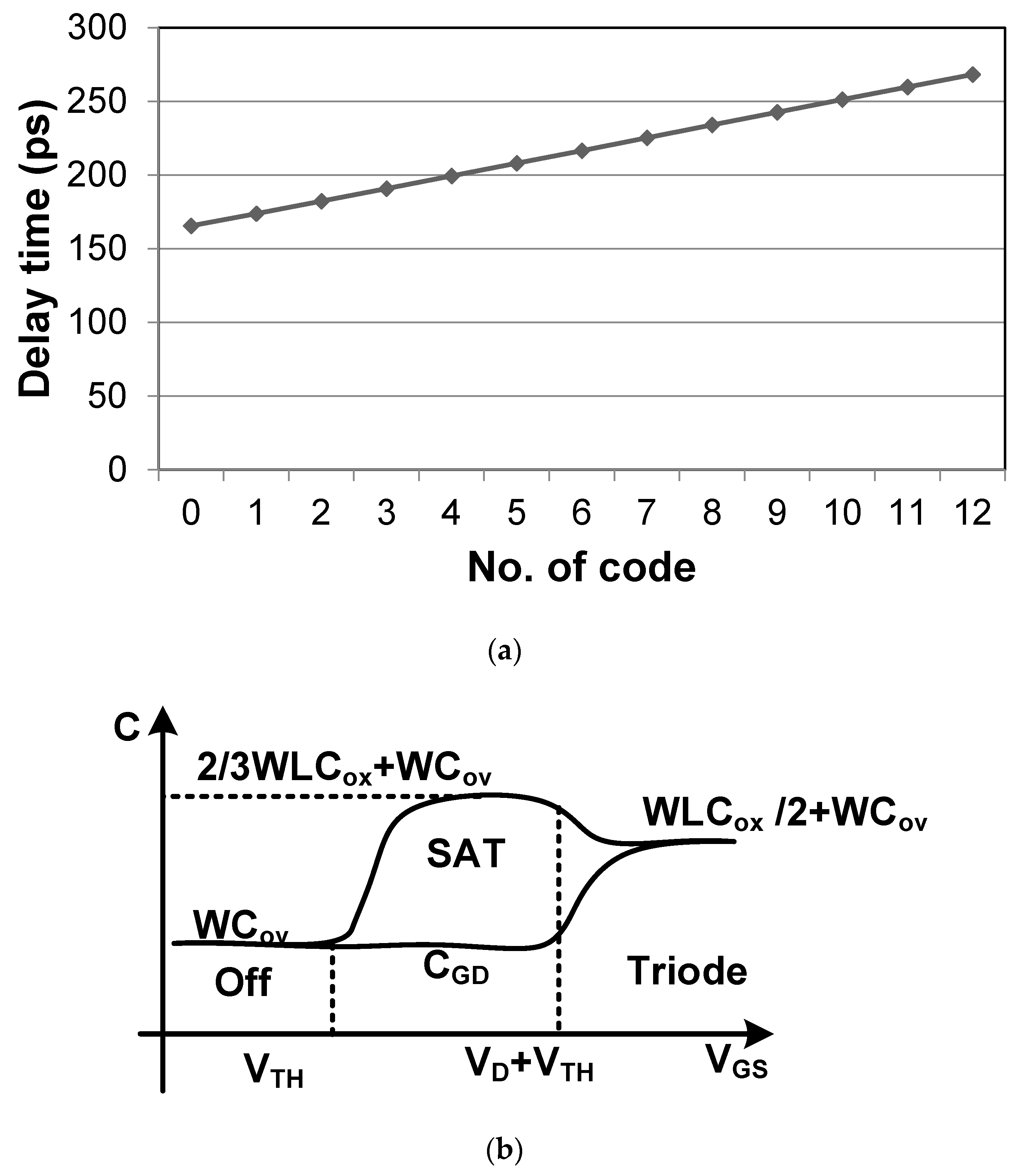
4.2. Fine Detector and Fine Delay Line
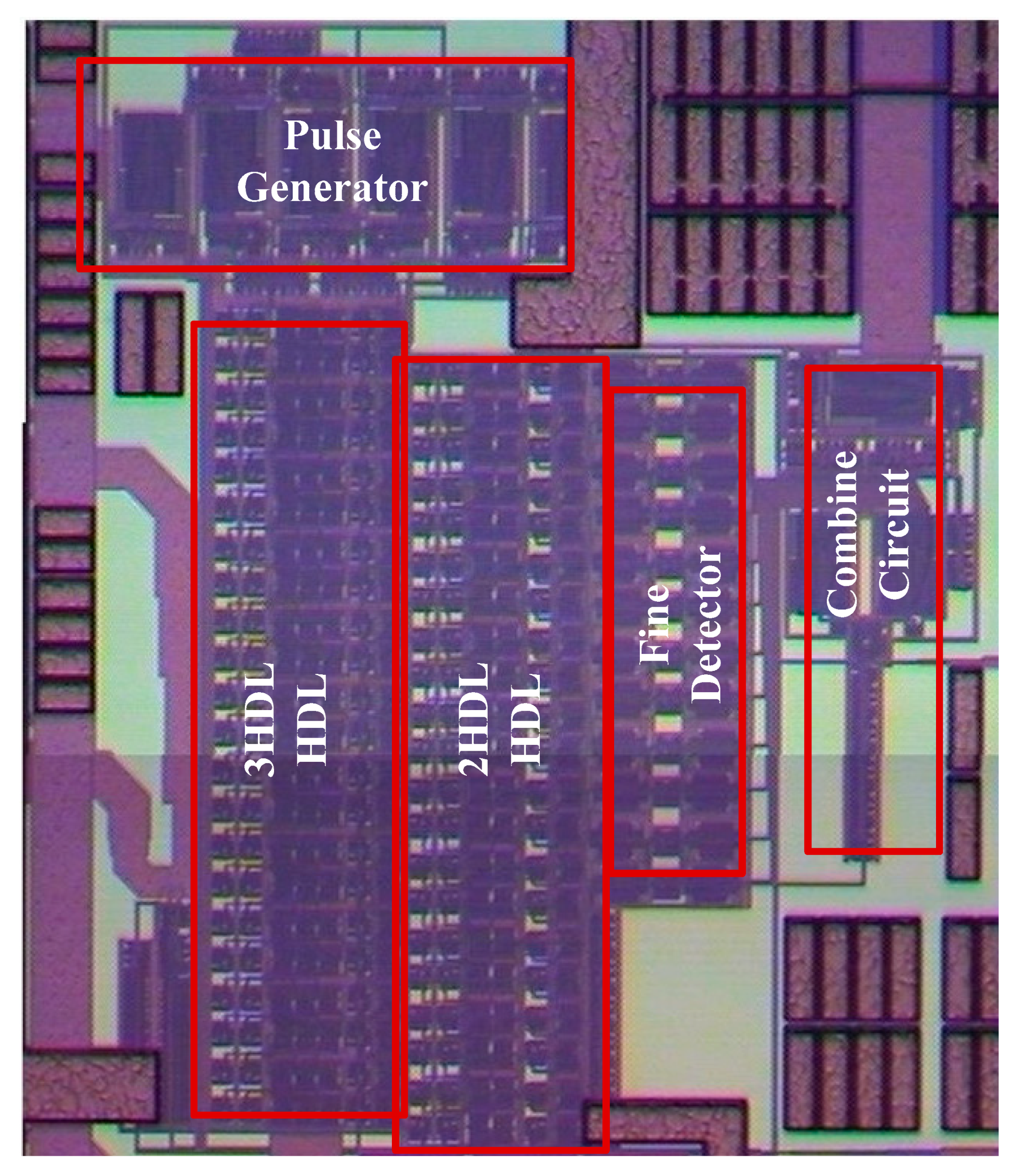
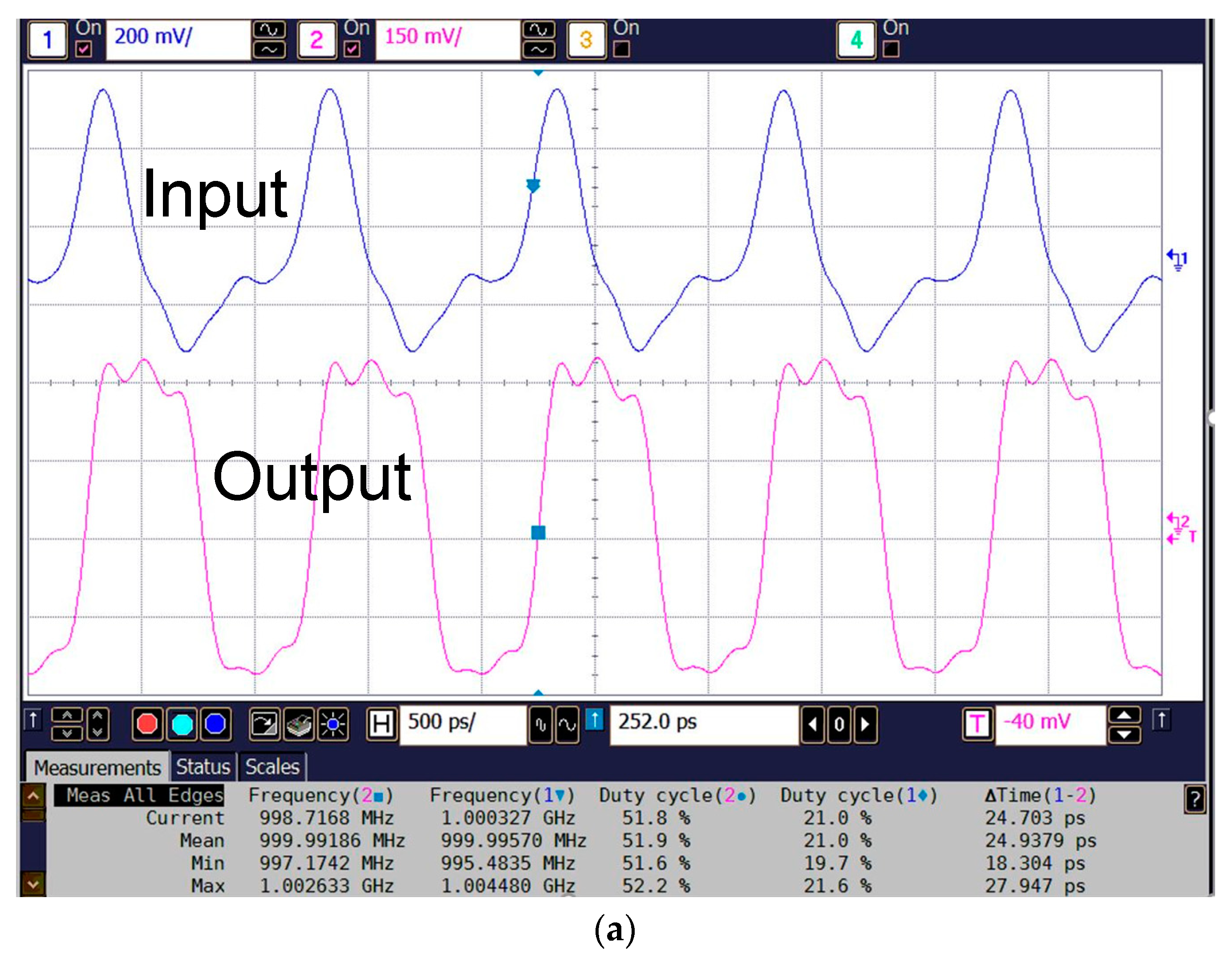
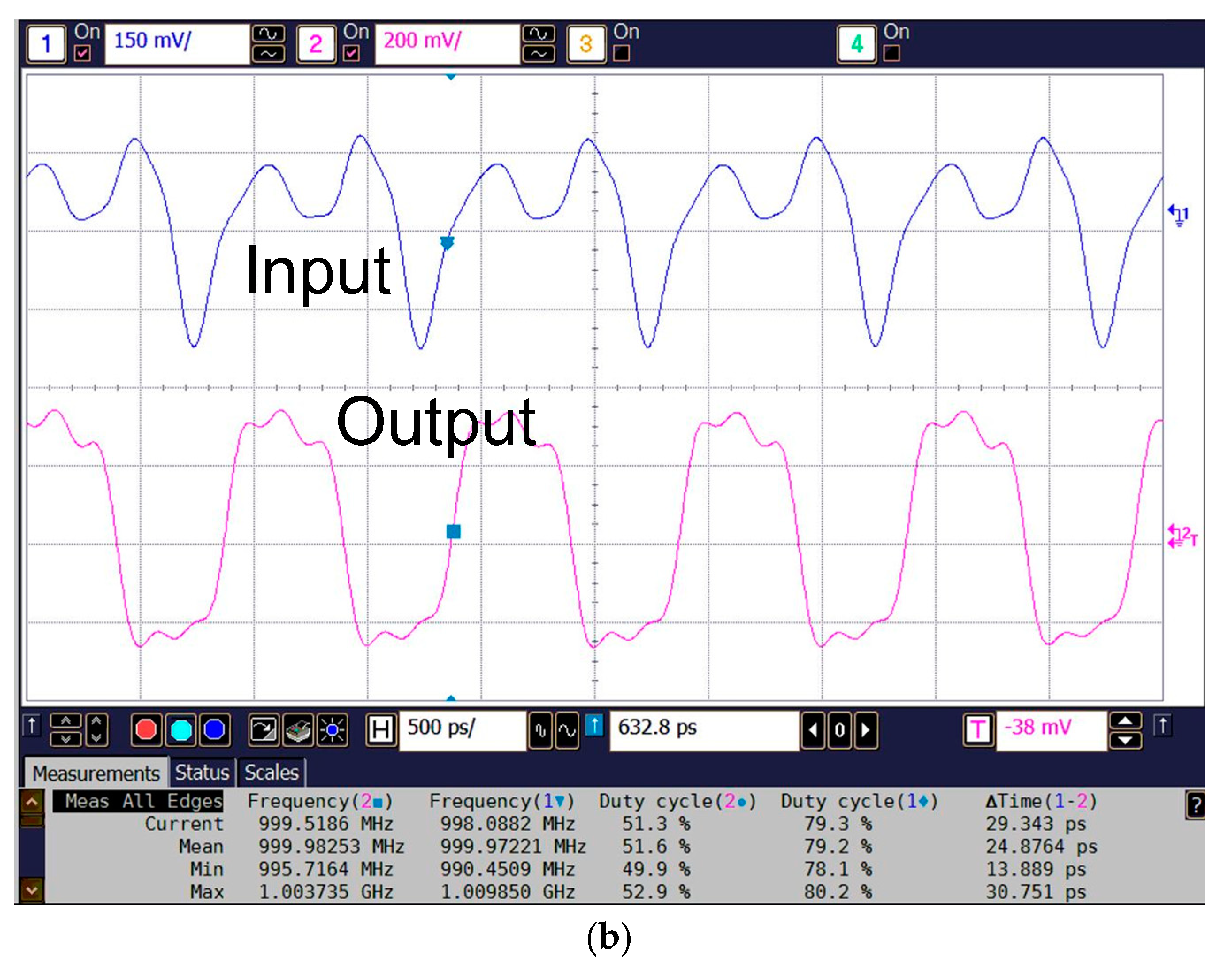
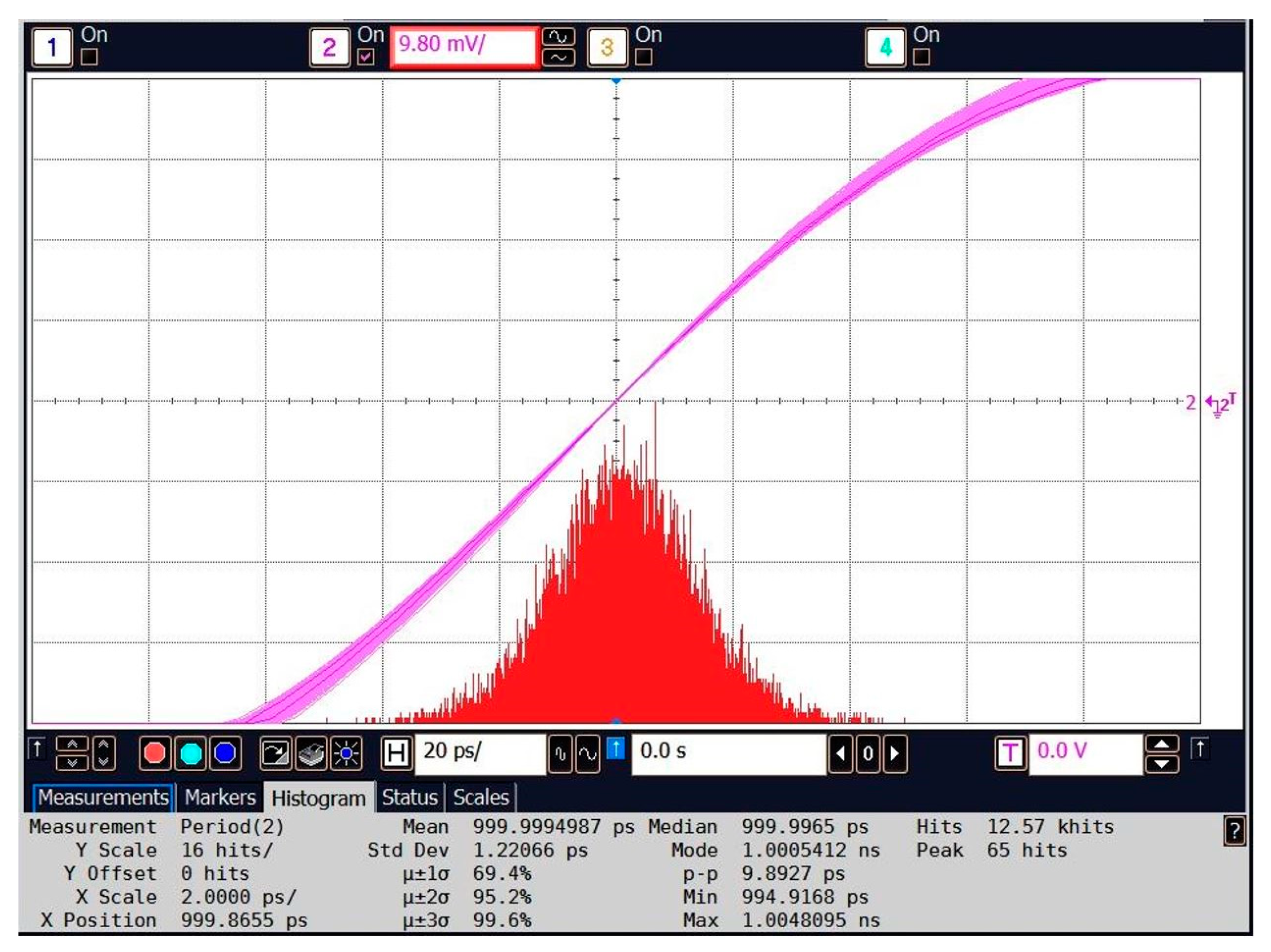
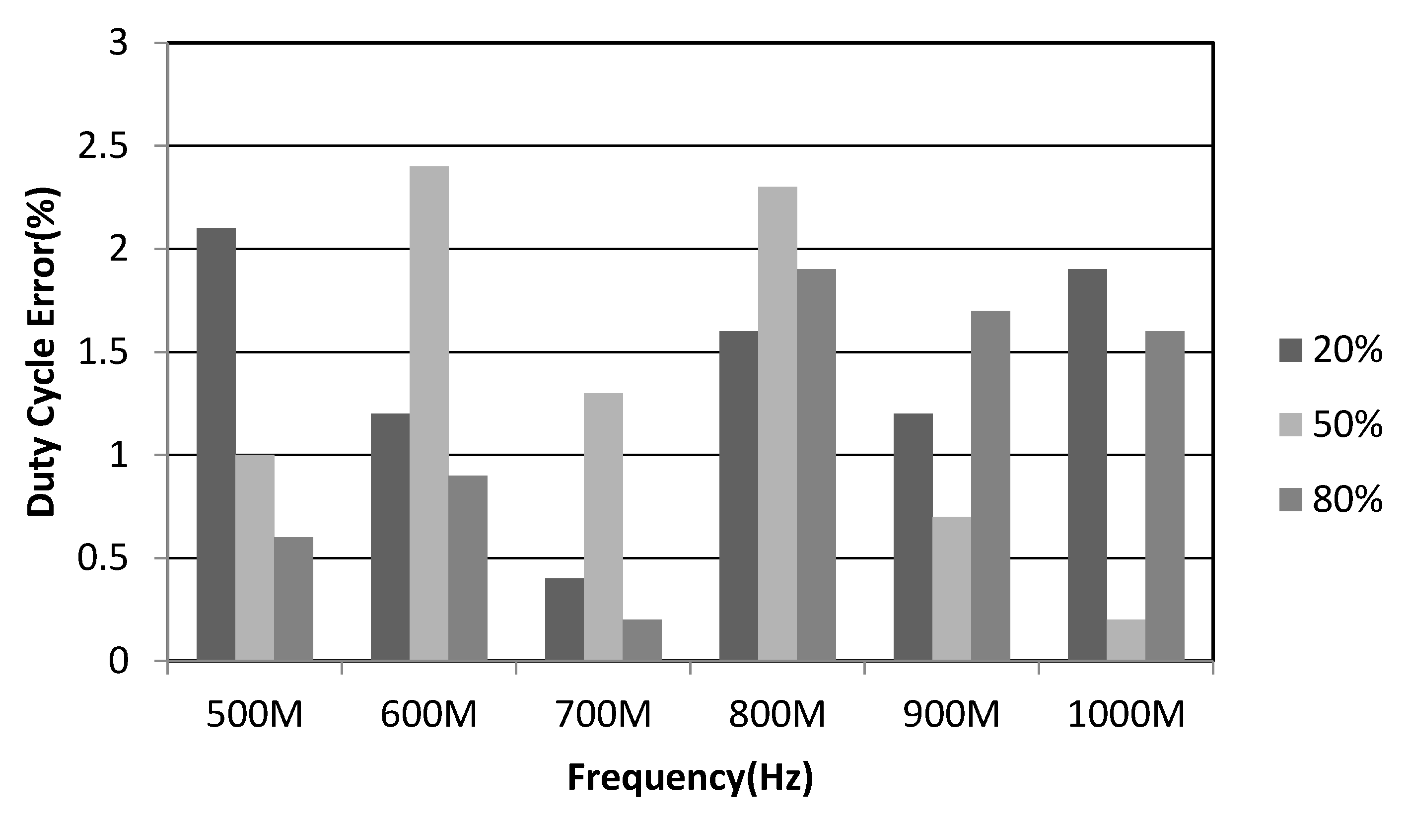
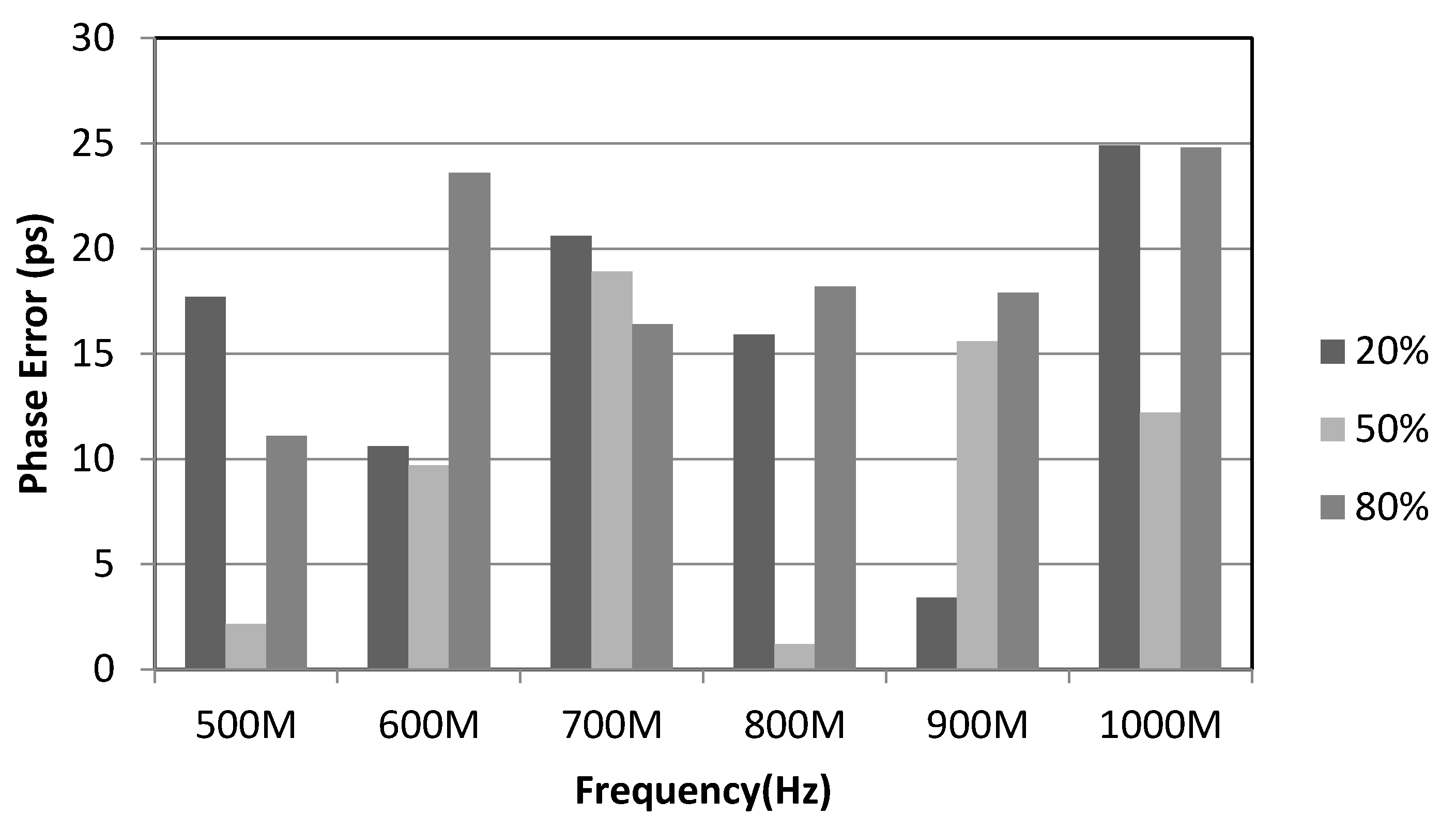
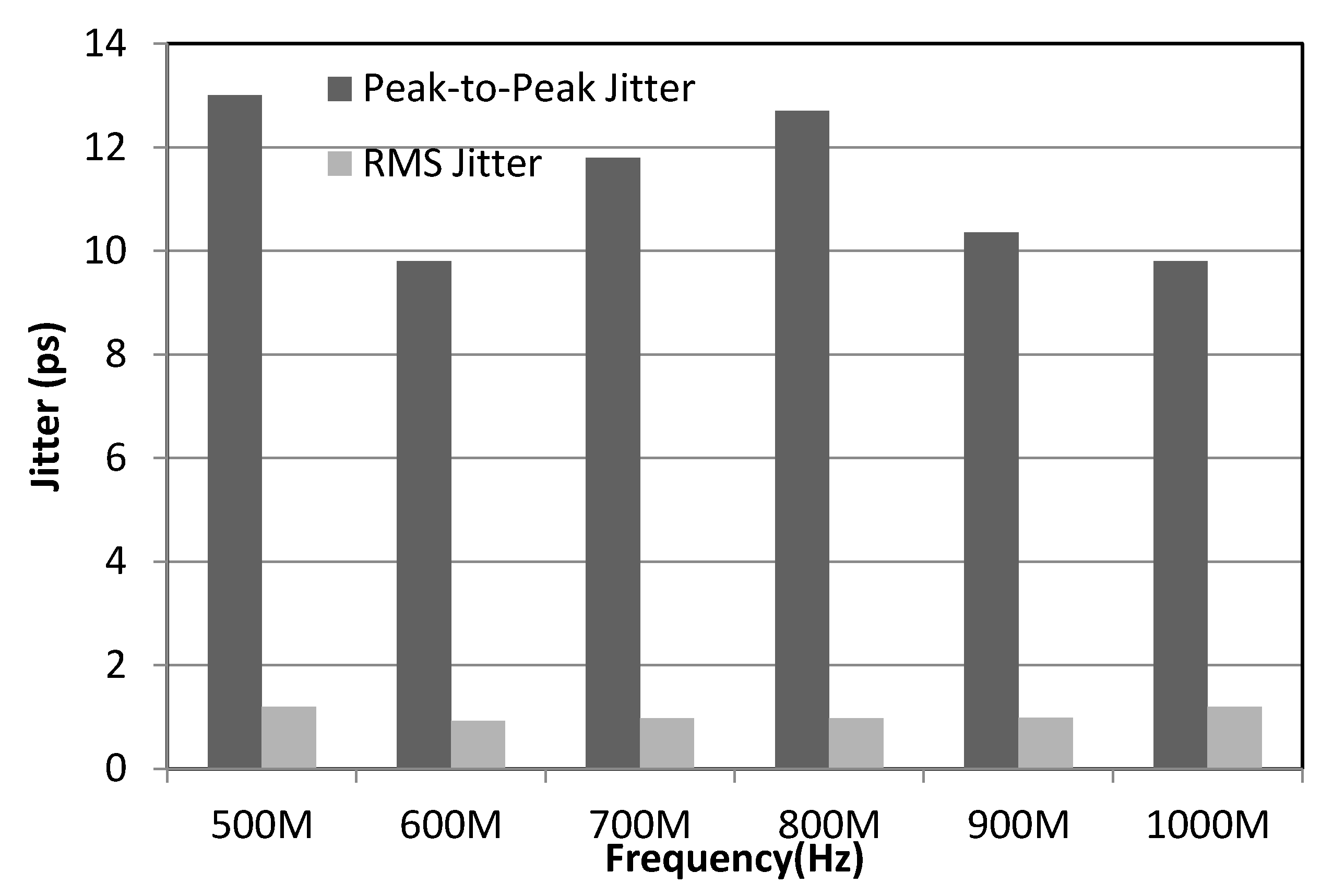
5. Experimental Results
6. Conclusions
Funding
Acknowledgments
Conflicts of Interest
References
- Young, I.; Greason, J.; Wong, K. A PLL clock generator with 5 to 110 MHz of lock rang for microprocessors. IEEE J. Solid-State Circuit 1992, 27, 1599–1607. [Google Scholar] [CrossRef]
- Bayer, M.; Chomicz, T.; Garg, N.; James, F.; McEntarfer, P.; Porter, J. Cell based fully integrated CMOS frequency synthesizers. IEEE J. Solid-State Circuits 1994, 29, 271–279. [Google Scholar]
- Chiu, W.; Huang, Y.; Lin, T. A Dynamic Phase Error Compensation Technique for Fast-Locking Phase-Locked Loops. IEEE J. Solid-State Circuits 2010, 45, 1137–1149. [Google Scholar] [CrossRef]
- Cheng, K.; Lo, Y. A Fast-lock Wide-Range Delay-Locked Loop Using Frequency-Rang Selector for Multiphase Clock Generator. IEEE Trans. Circuits Syst. II: Express Briefs 2007, 54, 561–565. [Google Scholar] [CrossRef]
- Chang, H.; Liu, D. A wide-range and fast-locking all-digital cycle-controlled delay-locked loop. IEEE J. Solid-State Circuits 2005, 40, 661–670. [Google Scholar] [CrossRef]
- Kao, S.; Cheng, H.; Lin, J. A self-calibrated delay-locked loop with low static phase error. Int. J. Circuit Theory Appl. 2016, 44, 929–944. [Google Scholar] [CrossRef]
- Mu, F.; Svensson, C. Pulsewidth control loop in high-speed CMOS clock buffers. IEEE J. Solid-State Circuits 2002, 35, 134–141. [Google Scholar]
- Lin, F. All digital duty-cycle correction circuit design and its applications in high-performance DRAM. In Proceedings of the 2011 IEEE Workshop on Microelectronics and Electron Devices, Boise, ID, USA, 22 April 2011; pp. 1–4. [Google Scholar]
- Lin, G.; Yang, C.; Lee, Y.; Weng, J. A Programmable Duty Cycle Corrector Based on Delta-Sigma Modulated PWM Mechanism. In Proceedings of the IEEE Pacific Conference Circuits and Systems, Macao, China, 30 November–3 December 2008; pp. 1406–1409. [Google Scholar]
- Liu, N.; Todsen, J.; Chen, D. A Low-Power and Area-Efficient Analog Duty Cycle Corrector for ADC’s External Clocks. In Proceedings of the IEEE International Symposium on Circuits and Systems (ISCAS), Sevilla, Spain, 11–14 October 2020; pp. 1–4. [Google Scholar]
- Zhang, J.; Meng, X. A 0.5–5 GHz 0.3-mW 50% duty-cycle corrector in 65-nm CMOS. In Proceedings of the IEEE Region 10 Conference (TENCON), Osaka, Japan, 16–19 November 2020; pp. 351–354. [Google Scholar]
- Shin, D.; Na, K.-J.; Kwon, D.; Kang, J.-H.; Song, T.; Jung, H.-D.; Lee, W.-Y.; Park, K.-C.; Park, J.-H.; Joo, Y.-S.; et al. Wide-Range Fast-Lock Duty-Cycle Corrector with Offset-Tolerant Duty-Cycle Detection Scheme for 54 nm 7 Gb/s GDDR5 DRAM Interface. In Proceedings of the 2009 Symposium VLSI Circuits, Kyoto, Japan, 16–18 June 2009; pp. 138–139. [Google Scholar]
- Swathi, R.; Srinivas, M.B. All Digital Duty Cycle Correction Circuit in 90nm based on Mutex. In Proceedings of the IEEE Computer Society Annual Symposium VLSI, Tampa, FL, USA, 13–15 May 2009; pp. 258–262. [Google Scholar]
- Kim, M.; Kim, L. A 100 MHz-to-1GHz Fast-Lock Synchronous Clock Generator with DCC for Mobile Applications. IEEE Trans. Circuits Syst. II Express Briefs 2011, 58, 477–481. [Google Scholar] [CrossRef]
- Shin, D.; Yun, W.J.; Lee, H.W.; Choi, Y.J.; Kim, S.; Kim, C. A 0.17–1.4GHz Low-Jitter All Digital DLL with TDC-based DCC using Pulse Width Detection Scheme. In Proceedings of the European Solid-State Circuits Conference, Edinburgh, UK, 15–19 September 2008; pp. 82–85. [Google Scholar]
- Chung, C.; Sheng, D.; Shen, S.E. High-Resolution All-Digital Duty-Cycle Corrector in 65-nm CMOS Technology. IEEE Trans. Very Large Scale Integr. (VLSI) Syst. 2014, 22, 1096–1195. [Google Scholar] [CrossRef]
- Chung, C.; Sheng, D.; Li, C. A Wide-Range Low-Cost All-Digital Duty-Cycle Corrector. IEEE Trans. Very Large Scale Integr. (VLSI) Syst. 2015, 23, 2487–2496. [Google Scholar] [CrossRef]
- Jeong, C.; Abdullah, A.; Min, Y.; Hwang, I.; Kim, S. All-Digital Duty-Cycle Corrector with a Wide Duty Correction Range for DRAM Applications. IEEE Trans. Very Large Scale Integr. (VLSI) Syst. 2016, 24, 363–367. [Google Scholar] [CrossRef]
- Chen, Y.; Tsao, H.; Hwang, C. A Fast-Locking All-Digital Deskew Buffer with Duty-Cycle Correction. IEEE Trans. Very Large Scale Integr. (VLSI) Syst. 2013, 21, 270–280. [Google Scholar] [CrossRef]
- Shin, D.; Song, J.; Chae, H.; Kim, C. A 7 ps Jitter 0.053 mm2 Fast Lock All-Digital DLL with a Wide Range and High Resolution DCC. IEEE J. Solid-State Circuits 2009, 44, 2437–2451. [Google Scholar] [CrossRef]
- Kang, K.; Kim, S.; Kim, S.J.; Lee, D.; Yoo, S.; Lee, K. A 0.33–1 GHz Open-Loop Duty Cycle Corrector with Digital Falling Edge Modulator. IEEE Trans. Circuits Syst. II Express Briefs 2018, 65, 1949–1953. [Google Scholar] [CrossRef]
- Chae, J.; Ko, H.; Park, J.; Kim, S. A Quadrature Clock Corrector for DRAM Interfaces, with a Duty-Cycle and Quadrature Phase Detector Based on a Relaxation Oscillator. IEEE Trans. Very Large Scale Integr. (VLSI) Syst. 2019, 27, 978–982. [Google Scholar] [CrossRef]


| [16] | [17] | [18] | [19] | [20] | [21] | [22] | This Work | |
|---|---|---|---|---|---|---|---|---|
| Process (μm) | 0.065 | 0.090 | 0.13 | 0.18 | 0.18 | 0.055 | 0.055 | 0.18 |
| Supply voltage (V) | 1 | 1 | 1.2 | 1.8 | 1.8 | 1 | 1 | 1.8 |
| Correction Range (%) | 14–86 | 9–86 | 10–90 | 30–70 | 20–80 | 20–80 | 38–54 | 20–80 |
| Frequency Range (GHz) | 0.262–1.02 | 0.075–0.734 | 0.350–1 | 0.250–0.625 | 0.440–1.5 | 0.333–1 | 1–3 | 0.5–1 |
| Locking Time (cycles) | 24 | <15 | 14 | <36 | 15 | <5 | <275 | <6 |
| Duty-Cycle Error (%) | 1.4 | 1.78 | <1.4 | <1.6 | ±1.8 | 2 | 0.8 | <1.9 |
| Phase error (ps) | 484 | 688.4 | NA | NA | –10.6 | NA | NA | 24.8 |
| Active Area (mm2) | 0.01 | 0.0289 | 0.059 | 0.09 | 0.053 | 0.016 | 0.003 | 0.0613 |
| Power Consumption (mW) | 6.5 | 4.59 | 5.6 | 10.8 | 43 | 2.09 | 2.08 | 10.1 |
| FOM | 0.431 | 0.594 | 0.57 | 11.52 | 1.11 | 0.09 | 0.27 | 0.382 |
Publisher’s Note: MDPI stays neutral with regard to jurisdictional claims in published maps and institutional affiliations. |
© 2021 by the author. Licensee MDPI, Basel, Switzerland. This article is an open access article distributed under the terms and conditions of the Creative Commons Attribution (CC BY) license (https://creativecommons.org/licenses/by/4.0/).
Share and Cite
Kao, S.-K. A 6-Locking Cycles All-Digital Duty Cycle Corrector with Synchronous Input Clock. Electronics 2021, 10, 860. https://doi.org/10.3390/electronics10070860
Kao S-K. A 6-Locking Cycles All-Digital Duty Cycle Corrector with Synchronous Input Clock. Electronics. 2021; 10(7):860. https://doi.org/10.3390/electronics10070860
Chicago/Turabian StyleKao, Shao-Ku. 2021. "A 6-Locking Cycles All-Digital Duty Cycle Corrector with Synchronous Input Clock" Electronics 10, no. 7: 860. https://doi.org/10.3390/electronics10070860
APA StyleKao, S.-K. (2021). A 6-Locking Cycles All-Digital Duty Cycle Corrector with Synchronous Input Clock. Electronics, 10(7), 860. https://doi.org/10.3390/electronics10070860