Abstract
This paper presents a design of a triangular slot-loaded planar rectangular antenna array for wideband millimeter-wave (mm-wave) 5G communication systems. The proposed array realizes an overall size of 35.5 × 14.85 mm2. To excite the array elements, a four-way broadband corporate feeding network was designed and analyzed. The proposed array offered a measured impedance bandwidth in two different frequency ranges, i.e., from 23 to 24.6 GHz and from 26 to 45 GHz. The single-antenna element of the array consists of a rectangular patch radiator with a triangular slot. The partial ground plane was used at the bottom side of the substrate to obtain a wide impedance bandwidth. The peak gain in the proposed array is ≈12 dBi with a radiation efficiency of >90%. Furthermore, the array gives a half-power beamwidth (HPBW) of as low as 12.5°. The proposed array has been fabricated and measured, and it has been observed that the measured results are in agreement with the simulated data.
1. Introduction
With the rapid growth in 4th generation (4G) communication systems, many research societies and industries are now focusing on future 5th generation (5G) communication systems [1]. It is expected that the upcoming 5G communication system exhibits a stable data-throughput experience over a wide range. With the allocation of an unlicensed spectrum currently at 28, 38, and 60 GHz frequency bands, it is possible to handle high data rates with low-cost infrastructure due to increased bandwidth. However, the earlier reported path loss models of millimeter-wave (mm-wave) channels suggest that there is a need to design an antenna system, which provides high bandwidth and high gain, and should be compact [2,3].
To achieve the above-mentioned objectives, the use of planar antennas would be beneficial. Planar antennas have gained a lot of attention in recent years for many microwave and mm-wave applications due to their small size, low fabrication cost, and easy integration for portable devices. At mm-wave frequencies, the small wavelength is an advantage for antenna designers to design compact and efficient antennas for 5G communication systems. Furthermore, it is realistic to design antennas that are physically small in size but electrically large enough to perform efficiently. However, the losses are high at mm-wave frequencies compared to microwave frequencies, so the design engineers need to be carefully select the substrate to minimize losses and achieve high radiation efficiency [4]. Moreover, the propagation loss is high at mm-wave frequencies due to the absorption of oxygen molecules. To overcome this problem, high gain antennas are required, and one of the techniques to enhance gain is to design antenna arrays. Previously, many researchers have presented different antenna array designs for 5G communication systems.
In [5], a dielectric resonator (DR)-loaded 1 × 4 substrate integrated waveguide (SIW) antenna array was presented for high-speed mm-wave communication systems. Two pieces of DR were placed on the H-shaped longitudinal slot, which was etched from the top metal layer. To feed array elements, a 50 Ω microstrip to SIW transition layer was placed on another side of the substrate. In [6], a dense dielectric (DD) patch antenna array design was presented for 28 GHz 5G communication systems. A 1-to-4 Wilkinson power divider was used to feed four element-based circular-shaped patch arrays. To improve radiation characteristics, an electromagnetic bandgap (EBG) structure-based ground plane was utilized and to improve the gain, a superstrate was employed above the array. In [7], a stacked patch antenna array structure was developed for 60 GHz applications. The presented single-antenna element consists of three different layers. An aperture-coupled patch antenna technique was utilized with a mounted horn. In [8], the authors also presented a series-fed aperture coupled patch antenna array for 60 GHz 5G communication systems.
In [9], an SIW-based antenna array design was presented for 28 GHz frequency band. The designed array consisted of three layers: the first layer comprised a broadband unequal feeding network; the second layer consisted of coupling slots, which are used to excite the radiating elements designed on the third layer. The cavity layer stacked between the second and third layers was utilized to achieve broadband performance. By utilizing the presented configuration, the authors achieved a maximum gain of 13.97 dBi with low cross-polarization and low side-lobe levels (SLLs). In [10], a novel wideband magneto-electric (ME) 1 × 4 dipole antenna array was designed and presented for 5G communication systems. The single element of the array consisted of a ME dipole excited using a slot coupled to a fork-shaped printed ridge gap waveguide. For gain enhancement, meta-lens consisted of three layers of split-ring resonators (SRRs) was used horizontally in front of the dipole element. The measured results showed that the antenna operates between 26.5 and 38.3 GHz, and it offered a measured realized gain of >15 dBi. In [11], a broadband mm-wave slot antenna array was designed for 5G communication systems. Two antenna arrays were designed to realize high gain and MIMO characteristics. Each array consisted of three antenna elements fed using a series feeding network. For gain enhancement, an EBG reflector was employed on the backside of the array. Although the antenna designs presented above provide a wide impedance bandwidth and high gain, their use is restricted in communication devices due to their bulky design configurations.
To overcome the above-mentioned problem, some of the researchers designed compact planar antenna arrays for different 5G frequency bands. In [12], a two-dimensional (2-D) array based on the concept of the Franklin linear array was presented for multiband mm-wave applications. The designed array had a triple band response at 28 GHz, 33 GHz, and 38 GHz with gain values of 13.5 dBi, 8.33 dBi, and 9.58 dBi, respectively. In [13], an inset-fed rectangular patch antenna array was presented for 28 GHz frequency band. To achieve wide impedance bandwidth and high gain, a parasitic patch was used on the top of each radiation element. Furthermore, the two consecutive array elements were placed perpendicular to each other to achieve high isolation between the antenna elements. Furthermore, the authors achieved a gain of about 20 dBi from the presented configuration. In [14], a novel and compact antipodal Vivaldi antenna (AVA) design was presented for broadband mm-wave applications. The antenna structure consisted of eight AVA antenna elements fed using a 1 × 8 T-junction power divider. The authors achieved an impedance bandwidth from 24.55 to 28.5 GHz and a gain of 6.96–11.32 dBi. For enhanced isolation between antenna elements, the authors utilized a notch on the ground plane.
In [15], a series-fed four-elements elliptical slot-based circular patch antenna array was presented for high-gain 5G communication systems. The elliptical slot was employed in the circular patch to achieve two resonant frequencies in the band of interest. Recently, Ullah and Tahir [16,17,18,19,20] designed and presented four-elements-based planar antenna arrays with different antenna structures for 5G communication systems. They also designed a broadband corporate feeding network to excite each array element. In their presented designs [16,17,18], they employed a wall of conducting vias around the antenna element to realize high isolation between the array elements.
In this paper, a planar antenna array has been presented for wideband 5G communication systems. The proposed array offers the advantages of low transmission loss, narrow half-power beamwidth (HPBW), and high gain with small size. The proposed broadband corporate feeding network is also simple to design and fabricate. The rest of the paper is organized in the following way. Section 2 presents a single-antenna element design along with the design procedure. Section 3 describes the design of the proposed feeding network and array configuration. Finally, Section 4 concludes the paper.
2. Antenna Design
2.1. Single Element
The top side of a single antenna element consists of a rectangular patch with a triangular slot, fed using a 50 Ω microstrip feed line, while the bottom side comprises a partial ground plane, as shown in Figure 1. The proposed wideband antenna is designed on Rogers RT/Duroid 5880 substrate with a thickness 0.51 mm, dielectric constant, = 2.2, and loss tangent, = 0.0009. The overall dimensions of a single antenna element are 5.5 × 7.5 mm2. The overall optimized design parameters are listed in Table 1.
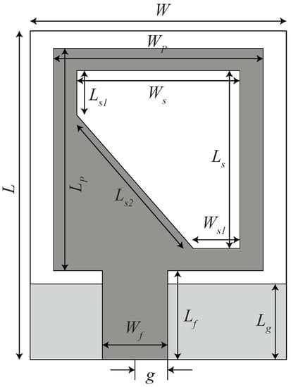
Figure 1.
Single-element antenna structure.

Table 1.
Optimized design parameters of single-antenna element (in mm).
2.2. Design Procedure
The design process of a single-antenna element consists of three major steps. These steps are named as antenna 1, antenna 2, and the proposed design, as depicted in Figure 2. Antenna 1 consists of a conventional rectangular patch element, which is fed through a 50 Ω microstrip feed line, as shown in Figure 2a. The bottom side of antenna 1 has a partial ground plane, which is designed to achieve wide impedance bandwidth. In antenna 2, a triangular slot (shown in Figure 2b) has been etched from a rectangular patch. In the final step, i.e., proposed design, shown in Figure 2c, the position of the microstrip feed line has been changed to improve the impedance matching at lower frequency bands. The step-by-step improvement in the reflection coefficient (S) of the single antenna element is depicted in Figure 3.
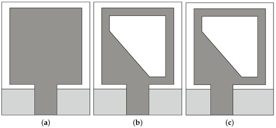
Figure 2.
Design process of the proposed single antenna element (a) antenna 1 (b) antenna 2 (c) proposed design.
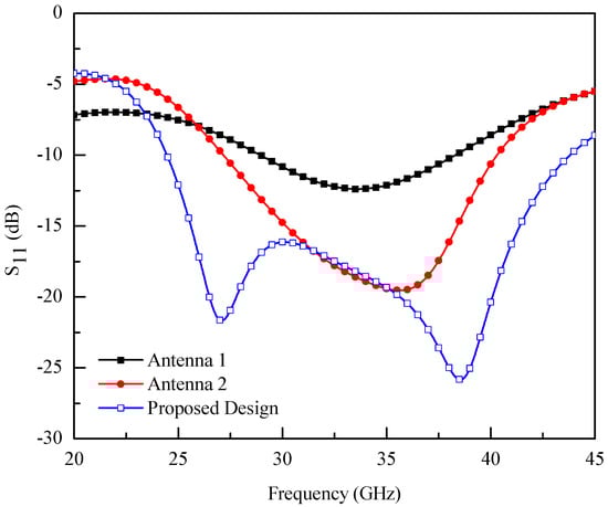
Figure 3.
Step-by-step improvement in S of single element antenna.
The targeted spectrum coverage is 28 and 38 GHz frequency bands. For this purpose, antenna 1, with rectangular patch and the partial ground plane, is designed as shown in Figure 2a. The rectangular patch has a length = 5 mm, which is ≈ at 28 GHz, where is the guided wavelength, while its width is = 4.5 mm. This configuration results in an impedance bandwidth that ranges from 28.95 to 38.275 GHz (i.e., BW = 9.325 GHz) with a resonance point at 33.57 GHz, as shown in Figure 3. After etching the triangular slot from the rectangular patch, as shown in Figure 2b, the bandwidth of the antenna improves by 3.8 GHz, ranging from 27.17 to 40.29 GHz (i.e., BW = 13.12 GHz) and its resonance point shifts towards 35.6 GHz. This effect can be seen from the graph of Figure 3 (red curve). The introduction of the triangular slot in the radiation element can provide two benefits: (1) the overall size of the antenna is reduced and (2) it excites higher-order modes in the design, which can lead to enhanced impedance bandwidth.
When the position of the feed line shifts by 0.5 mm from the normal position, shown in Figure 2c (proposed design), the antenna impedance bandwidth further improves by 6.18 GHz in the frequency range of 24.5–43.8 GHz (i.e., BW = 19.3 GHz), and it provides two resonance points at 27 GHz and 38.5 GHz, as shown in Figure 3. The change in the feed line position will initiate a capacitive effect in the patch radiator, which ultimately reduces the inductive effect results in a purely resistive impedance, and enhances the impedance bandwidth. This can be observed from Figure 4a, where a parametric study is presented by changing the feed line position. From the figure, it can be noted that when the feed line is positioned on its normal location ( and ), the antenna resonates at a center frequency of 35 GHz and provides an impedance bandwidth from 28 to 40 GHz. When the feed line position is changed up to 0.5 mm, an enhanced impedance bandwidth is observed. For values greater than 0.5 mm, the bandwidth of the antenna reduces and, ultimately, its resonance shifts towards lower bands. Therefore, one can say that the electrical length of the antenna increases when the feed line position is shifted towards its maximum value.
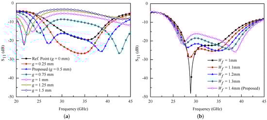
Figure 4.
Effect of (a) g and (b) on antenna’s performance.
The effect of feed line width () on the antenna’s performance is shown in Figure 4b. The value of is increased from 1 mm to 1.4 mm with a step size of 0.1 mm. One can observe from Figure 4b that the bandwidth of the antenna also increased with the increase in . Therefore, for the proposed design, is chosen to be 1.4 mm.
Figure 5a illustrates the effect of on antenna’s performance. From the figure, it can be observed that when the value of increases from 2 mm to 4 mm, the lower frequency limit is extended from 25.55 GHz to 24.37 GHz. On the other hand, from Figure 5b, it can be observed that the antenna’s impedance bandwidth is almost equal when the value of increases from 1.5 mm to 3.5 mm. It can also be observed from Figure 5a,b, that for = 4 mm and = 3.5 mm, the antenna resonates for the bands of interest, i.e., 28 GHz and 38 GHz.
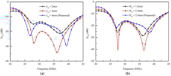
Figure 5.
Effect of (a) and (b) on antenna’s performance.
To validate the proposed methodology, the surface current distribution of the proposed planar antenna is plotted and shown in Figure 6. It has been observed from the figure that the use of a triangular slot and the shift in feed line position generates two different paths for the surface current, which results in two resonant points. In the case of 27 GHz, the maximum current is distributed around the base and perpendicular side of the triangular slot, while for 38.5 GHz, a dense current is distributed around the hypotenuse of the triangular slot. Therefore, it is worth mentioning that the triangular slot plays an important role in achieving a wideband response with two resonant points, i.e., 27 GHz and 38.5 GHz.
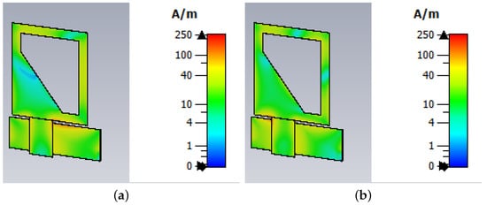
Figure 6.
Simulated surface current distribution of the proposed planar antenna at (a) 27 GHz and (b) 38.5 GHz.
The radiation characteristics of a single-antenna element are shown in Figure 7 for resonant frequencies 27 GHz and 38.5 GHz. From Figure 7a, one can observe that the proposed antenna has typical monopole-like radiations in both E- and H-plane. For 38.5 GHz, shown in Figure 7b, directional radiation patterns are observed for both planes.
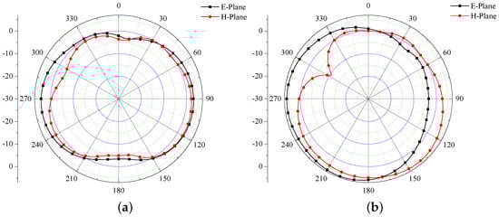
Figure 7.
Simulated radiation characteristics of single antenna element at (a) 27 GHz and (b) 38.5 GHz.
The simulated gain and radiation efficiency of a single-antenna element are illustrated in Figure 8. The proposed antenna offers a radiation efficiency of more than 75% and the gain varies linearly between 3.2 and 5.7 dBi in the entire operating band. The minimum gain value is noted to be 3.2 dBi at 24.5 GHz, while the maximum gain is 5.25 dBi at 43.8 GHz, as shown in Figure 8.
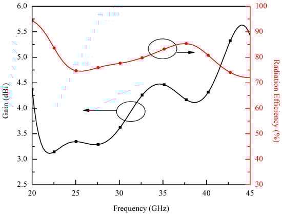
Figure 8.
Simulated gain and radiation efficiency of single antenna element.
3. Feed Network and Array Design
This section describes the design of the proposed feeding network and antenna array. The feeding network plays a crucial role in designing the antenna array, so its design and analysis should be considered first. Therefore, for the proposed array, a four-way planar broadband corporate feeding network has been designed, as shown in Figure 9.
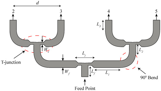
Figure 9.
Structure of the proposed four-way broadband feeding network.
The purpose behind the feeding network is to provide each antenna element input waveform with equal magnitude and phase. The proposed feeding network has one input and four output ports. It consists of three distinct parts, i.e., microstrip lines, 90 bends, and T-junctions. The design starts with the realization of a microstrip feed line whose characteristic impedance () is 50 at 28 GHz. The S11 of the microstrip line is ≤−40 dB over the entire frequency range, as shown in Figure 10a, while its transmission coefficient (S21) is ≈0 dB, as shown in Figure 10b. For routing multiple feed lines in the system, several 90 bends have to be utilized. While designing the 90 bend, it should be noted that its respective reflection coefficient should be less than 10 dB, which is also clear from the result of Figure 10a. The optimized values of the 90 bend are: = 1.4 mm and radius (r) = 2 mm. The magnitude of S of 90 bend is shown in Figure 10b, and it is also ≈0 dB that indicates maximum power transfer at the output ports. T-junction is the most important part of any feeding network. The main purpose of the T-junction is to provide 3 dB power division and zero phases at the output ports. The structure of the designed T-junction power divider is also shown in Figure 9. The S shown in Figure 10a indicates that the T-junction has less than −10 dB response over a broad range from 20 to 40 GHz. Furthermore, the transmission coefficients of the proposed T-junction, shown in Figure 10b, are better than 3.5 dB for the entire operating range.
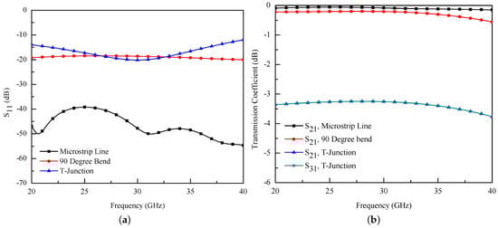
Figure 10.
Simulated (a) reflection and (b) transmission coefficients of different parts of the feed network.
To provide isolation between the array elements, the gap d between the elements is chosen to be 9.6 mm, which is greater than at the lowest operating frequency, where is the free-space wavelength. It also ensures that no grating lobes are formed at this frequency or above this point. Rest of the optimized design parameters are: = 2, = 3.8, = 0.45, = 5.2, = 1, and = 0.5 (in mm). The proposed feeding network has been simulated in the CST Microwave Studio, and the S parameter is shown in Figure 11. From the figure, one can observe that the proposed feeding network has S magnitude less than 10 dB for the desired frequency range, i.e., from 20 to 40 GHz. On the other hand, Figure 12 illustrates the transmission coefficients of the proposed four-way broadband feeding network. It has been noted from the result of Figure 12 that the power distribution ratio is in the range of 6–7 dB.
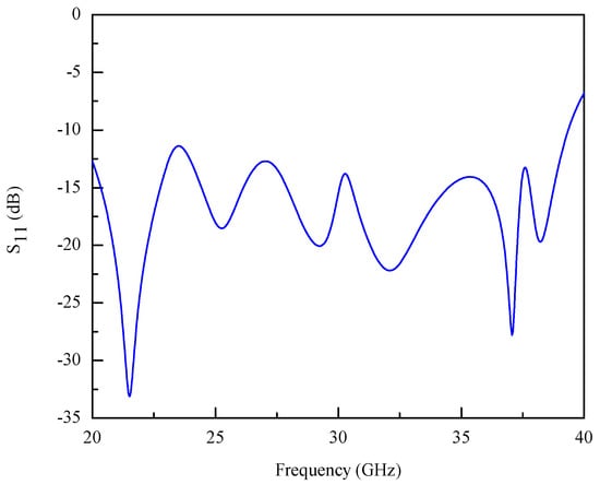
Figure 11.
Simulated S of the proposed four-way broadband feeding network.
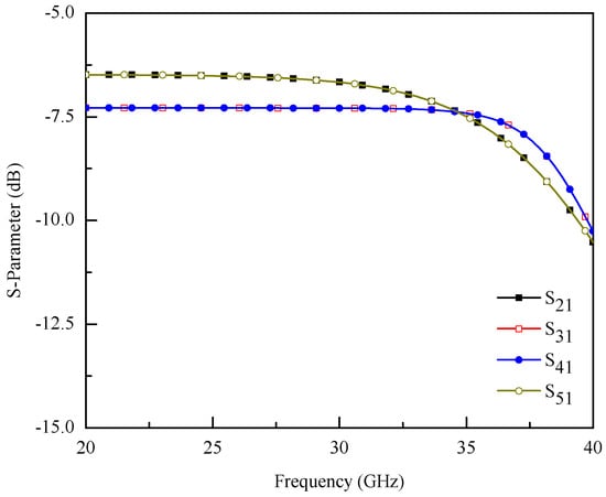
Figure 12.
Simulated transmission coefficients of the proposed four-way broadband feeding network.
After designing a feeding network, multiple single antenna elements and feeding network are combined to realize the final array, as shown in Figure 13. The overall dimensions of the array are W = 35.5 mm and L = 14.85 mm.
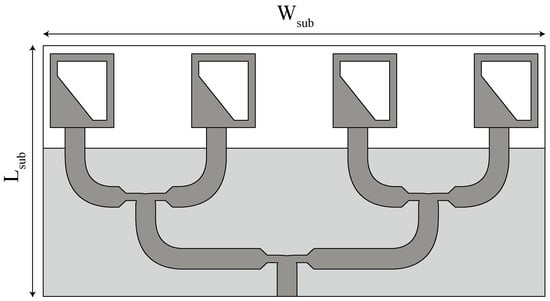
Figure 13.
Proposed four element antenna array.
4. Simulated and Measured Results
The proposed four-element antenna array has been designed and simulated in CST Microwave Studio, and fabricated on 0.51 mm thick Rogers RT/Duroid 5880 substrate. The fabricated prototype of the proposed array is shown in Figure 14. A Cinch Connectivity Solutions 2.92 mm End Launch RF Connector has been used for array testing, as shown in Figure 14. Furthermore, to validate the simulation results, the prototype, shown in Figure 14, is measured using Agilent Technologies Power Network Analyzer (PNA) N5245B. The length of the microstrip feed line has been increased from 2 to 10 mm to effectively use the RF connector. The array with a 10 mm microstrip feed line is also modeled in CST and S is plotted along with the original feed length, as shown in Figure 15. The comparison between the simulated and measured S of the proposed antenna array is also shown in Figure 15. From the figure, one can observe that for both the feed lines, i.e., 2 mm and 10 mm, the array offers almost equal results. From this result, one can also observe that the designed array provides two different impedance bandwidths, i.e., from 23 to 24.6 GHz and from 26 to 45 GHz. The measured S are in good agreement with the simulated one. Furthermore, from the results of Figure 15, it can be noted that the antenna array offers multiple resonances in the band of interest. The discrepancies between the results could arise due to fabrication intolerances and RF connector losses.
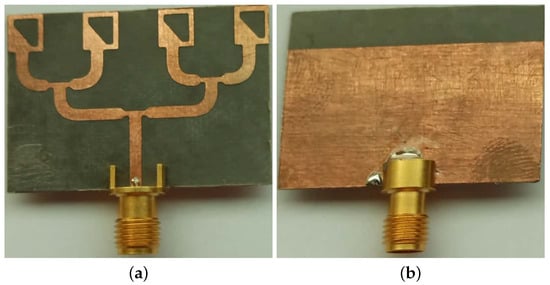
Figure 14.
(a) Front view and (b) back view of the fabricated prototype of the proposed four element antenna array.
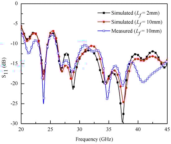
Figure 15.
Simulated and measured S of the proposed four element antenna array.
The radiation efficiency and gain of the proposed array are shown in Figure 16. The proposed antenna array offers a simulated radiation efficiency of more than 90% for the entire frequency band, while the measured radiation efficiency varies in the range of 84–95% from 27 to 37.5 GHz. From simulations, the average gain of the proposed array is noted to be ≈9.5 dBi from 26 to 35 GHz, and it increases linearly up to 12 dBi at 40 GHz. Furthermore, the measured gain shows an average value of 9.5 dBi from 27 to 37.5 GHz.
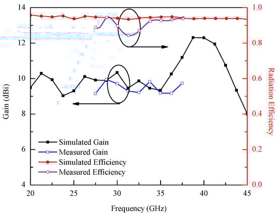
Figure 16.
Simulated and measured gain, and radiation efficiency of the proposed four element antenna array.
The simulated and measured radiation characteristics of the proposed antenna array are shown in Figure 17 for resonant frequencies 28.5 GHz and 37.5 GHz. From Figure 17a,b, one can observe that the main beam is directed towards 0 in the E- and H-plane. In the case of an E-plane, the HPBW is noted to be 12.5. For 38.5 GHz, shown in Figure 17c,d, the maximum radiation occurs at 60 and 330 in E-plane with the HPBW of 23. The radiation null is in the end-fire direction with a magnitude of −10 dB. In H-plane, for 38.5 GHz, the array offers directional radiation characteristics. The main beam is shifted from the end-fire direction and tilted towards 26 in H-plane. From Figure 17a–d, one can also observe that the simulated and measured radiation characteristics are in agreement.
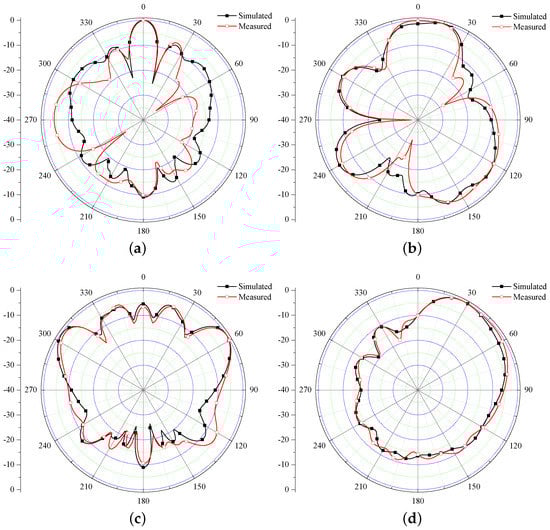
Figure 17.
Simulated and measured radiation characteristics of the proposed four element antenna array (a) for E-plane at 28.5 GHz (b) for H-plane at 28.5 GHz (c) for E-plane at 37.5 GHz (d) for H-plane at 37.5 GHz.
A comparison between proposed and previously presented planar antenna arrays is given in Table 2. The comparison is done in terms of array size, array elements, operating frequency range, bandwidth, efficiency, and peak gain. From the data of the table, it can be noted that the proposed planar array is compact and it offers a wide impedance bandwidth with acceptable gain compared to previously presented designs. Although the gain of the antenna can be increased by increasing the number of array elements, as described by [13], it will increase the overall array size, which is not useful for compact communication devices. This effect can be justified from the result of Figure 18, where a comparison is provided between the gain of four-elements and eight-elements antenna arrays. From the results of Figure 18, one can observe that an ≈3 dB improvement has been observed in the gain value when the number of elements in the array increases.
Table 2.
Comparison between proposed and previously presented planar antenna arrays.
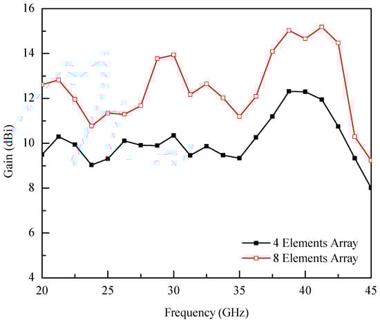
Figure 18.
Comparison between four and eight elements array gain.
5. Conclusions
A four-element (1 × 4) antenna array is presented for upcoming 5G communication systems. The single element of the array consisted of a rectangular patch radiator with a triangular slot and a partial ground plane. It has been described that, by utilizing a triangular slot, and by changing the position of the feed line, an enhanced impedance bandwidth has been achieved, from 26 to 45 GHz, which includes the most prominent 28 and 38 GHz 5G bands. A four-way broadband corporate feeding network is proposed to evaluate the performance of the array. From simulation and measurement results, it can be observed that the designed array offers a peak gain of 12 dBi, and radiation efficiency of >90% for the entire frequency range. The presented array is fabricated and measured, and it can be observed that the measured results showed excellent similarity with the simulated data. Furthermore, the presented array design is compact, simple to fabricate, and offers a high gain that makes it a good candidate for future 5G communication systems.
Author Contributions
Conceptualization, I.A.; methodology, I.A., H.S. and U.R.; software, I.A. and U.R.; validation, U.R. and Z.Y.; formal analysis, Z.Y.; investigation, H.S. and Z.Y.; resources, U.R.; writing—original draft preparation, I.A.; writing—review and editing, U.R. and Z.Y.; visualization, U.R.; supervision, H.S.; project administration, H.S. and Z.Y. All authors have read and agreed to the published version of the manuscript.
Funding
This research received no external funding.
Conflicts of Interest
The authors declare no conflict of interest.
References
- Rappaport, T.S.; Sun, S.; Mayzus, R.; Zhao, H.; Azar, Y.; Wang, K.; Wong, G.N.; Schulz, J.K.; Samimi, M.; Gutierrez, F., Jr. Millimeter wave mobile communications for 5G cellular: It will work! IEEE Access 2013, 1, 335–349. [Google Scholar] [CrossRef]
- Osseiran, A.; Boccardi, F.; Braun, V.; Kusume, K.; Marsch, P.; Maternia, M.; Queseth, O.; Schellmann, M.; Schotten, H.; Taoka, H.; et al. Scenarios for 5G mobile and wireless communications: The vision of the METIS project. IEEE Commun. Mag. 2014, 52, 26–35. [Google Scholar] [CrossRef]
- Sulyman, A.I.; Nassar, A.T.; Samimi, M.K.; MacCartney, G.R.; Rappaport, T.S.; Alsanie, A. Radio propagation path loss models for 5G cellular networks in the 28 GHz and 38 GHz millimeter-wave bands. IEEE Commun. Mag. 2014, 52, 78–86. [Google Scholar] [CrossRef]
- Alhalabi, R.A. High efficiency planar and RFIC-based antennas for millimeter-wave communication systems. Ph.D. Thesis, UC San Diego, San Diego, CA, USA, 2010. [Google Scholar]
- Ashraf, N.; Vettikalladi, H.; Alkanhal, M.A. A DR loaded substrate integrated waveguide antenna for 60 GHz high speed wireless communication systems. Int. J. Antennas Propag. 2014, 2014, 146301. [Google Scholar] [CrossRef]
- Haraz, O.M.; Elboushi, A.; Alshebeili, S.A.; Sebak, A.-R. Dense dielectric patch array antenna with improved radiation characteristics using EBG ground structure and dielectric superstrate for future 5G cellular networks. IEEE Access 2014, 2, 909–913. [Google Scholar] [CrossRef]
- Vettikalladi, H.; Sethi, W.T.; Alkanhal, M.A. High gain and high efficient stacked antenna array with integrated horn for 60 GHz communication systems. Int. J. Antennas Propag. 2014, 2014, 418056. [Google Scholar] [CrossRef]
- Mohamed, I.; Sebak, A.R. High-gain series-fed aperture-coupled microstrip antenna array. Micro. Optical Tech. Lett. 2015, 57, 91–94. [Google Scholar] [CrossRef]
- Park, S.-J.; Shin, D.-H.; Park, S.-O. Low side-lobe substrate integrated-waveguide antenna array using broadband unequal feeding network for millimeter-wave handset device. IEEE Trans. Antennas Propag. 2015, 64, 923–932. [Google Scholar] [CrossRef]
- Dadgarpour, A.; Sorkherizi, M.S.; Kishk, A.A. Wideband low-loss magnetoelectric dipole antenna for 5G wireless network with gain enhancement using meta lens and gap waveguide technology feeding. IEEE Trans. Antennas Propag. 2016, 64, 5094–5101. [Google Scholar] [CrossRef]
- Saad, A.A.R.; Mohamed, H.A. Printed millimeter-wave MIMO based slot antenna arrays for 5G networks. AEU-Int. J. Elect. Commun. 2019, 99, 59–69. [Google Scholar] [CrossRef]
- Jilani, S.F.; Alomainy, A. A multiband millimeter-wave 2-D array based on enhanced Franklin antenna for 5G wireless systems. IEEE Antennas Wirel. Propag. Lett. 2017, 16, 2983–2986. [Google Scholar] [CrossRef]
- Khalily, M.; Tafazolli, R.; Xiao, P.; Kishk, A.A. Broadband mm-Wave microstrip array antenna with improved radiation characteristics for different 5G applications. IEEE Trans. Antennas Propag. 2018, 66, 4641–4647. [Google Scholar] [CrossRef]
- Zhu, S.; Liu, H.; Chen, Z.; Wen, P. A compact gain-enhanced vivaldi antenna array with suppressed mutual coupling for 5G mmWave application. IEEE Antennas Wirel. Propag. Lett. 2018, 17, 776–779. [Google Scholar] [CrossRef]
- Khattak, M.I.; Sohail, A.; Khan, U.; Barki, Z.; Witjaksono, G. Elliptical slot circular patch antenna array with dual band behaviour for future 5G mobile communication networks. Prog. Electromagn. Res. 2019, 89, 133–147. [Google Scholar] [CrossRef]
- Ullah, H.; Tahir, F.A. A broadband wire hexagon antenna array for future 5G communications in 28 GHz band. Micro. Optical Tech. Lett. 2019, 61, 696–701. [Google Scholar] [CrossRef]
- Ullah, H.; Tahir, F.A. Broadband planar antenna array for future 5G communication standards. IET Microw. Antennas Propag. 2019, 13, 2661–2668. [Google Scholar] [CrossRef]
- Ullah, H.; Tahir, F.A. A wide-band rhombus monopole antenna array for millimeter wave applications. Micro. Optical Tech. Lett. 2020, 62, 2111–2117. [Google Scholar] [CrossRef]
- Ullah, H.; Tahir, F.A. A high gain and wideband narrow-beam antenna for 5G millimeter-wave applications. IEEE Access 2020, 8, 29430–29434. [Google Scholar] [CrossRef]
- Ullah, H.; Tahir, F.A. A novel snowflake fractal antenna for dual-beam applications in 28 GHz band. IEEE Access 2020, 8, 19873–19879. [Google Scholar] [CrossRef]
Publisher’s Note: MDPI stays neutral with regard to jurisdictional claims in published maps and institutional affiliations. |
© 2021 by the authors. Licensee MDPI, Basel, Switzerland. This article is an open access article distributed under the terms and conditions of the Creative Commons Attribution (CC BY) license (http://creativecommons.org/licenses/by/4.0/).