Abstract
A split-gate metal–oxide–semiconductor field-effect transistor (SG-DMOSFET) is a well-known structure used for reducing the gate–drain capacitance (CGD) to improve switching characteristics. However, SG-DMOSFETs have problems such as the degradation of static characteristics and a high gate-oxide electric field. To solve these problems, we developed a SG-DMOSFET with floating p+ polysilicon (FPS-DMOSFET) and compared it with a conventional planar DMOSFET (C-DMOSFET) and a SG-DMOSFET through Technology Computer-Aided Design (TCAD) simulations. In the FPS-DMOSFET, floating p+ polysilicon (FPS) is inserted between the active gates to disperse the high drain voltage in the off state and form an accumulation layer over the entire junction field effect transistor (JFET) region, similar to a C-DMOSFET, in the on state. Therefore, the FPS-DMOSFET can minimize the degradation of static characteristics such as the breakdown voltage (BV) and specific on resistance (RON,SP) in the split-gate structure. Consequently, the FPS-DMOSFET can shorten the active gate length and achieve a gate-to-drain capacitance (CGD) that is less than those of the C-DMOSFET and SG-DMOSFET by 48% and 41%, respectively. Moreover, the high-frequency figure of merit (HF-FOM = RON,SP × CGD) of the FPS-DMOSFET is lower than those of the C-DMOSFET and SG-DMOSFET by 61% and 49%, respectively. In addition, the FPS-DMOSFET shows an EMOX of 2.1 MV/cm, which guarantees a gate oxide reliability limit of 3 MV/cm. Therefore, the proposed FPS-DMOSFET is the most appropriate device to be used in high-voltage and high-frequency electronic applications.
1. Introduction
4H-SiC metal-oxide-semiconductor field-effect transistors (MOSFETs) are considered promising candidates for high-temperature and high-voltage applications [1,2]. Recently, several studies have been conducted on trench MOSFETs (UMOSFESTs) owing to their high channel mobility and small cell pitch [3,4,5]. However, a high gate-oxide electric field occurs at the trench gate corner, leading to reliability issues in the gate oxide. To achieve stable operation, the maximum electric field in the gate oxide (EMOX) must be lower than 3 MV/cm [6]. In addition, the gate–drain capacitance (CGD) and gate–drain charge (QGD) of trench MOSFETs are higher than those of planar MOSFETs (DMOSFESTs) due to the large cell density. Furthermore, in high-voltage applications (>3.3 kV), the channel resistance of trench MOSFETs does not have a significant effect on the overall resistance owing to the thick drift region [7]. Therefore, planar MOSFETs are more suitable for high-voltage and high-frequency applications.
The high-frequency performance of SiC MOSFETs is generally evaluated using the high-frequency figure of merit (HF-FOM), which is calculated as RON,SP × QGD or RON,SP × CGD, where RON,SP is the specific on resistance. A well-known method for reducing CGD is the use of the split-gate MOSFET (SG-MOSFET) structure [8,9], which is shown in Figure 1b. This structure improves HF-FOM through reduction of CGD by decreasing the active gate length protruding into the n-drift region (LSG). However, this structure substantially decreases Baliga’s figure of merit (BFOM), which is calculated as BV2/RON,SP [10]. In particular, SG-DMOSFETs have a serious problem of a high EMOX at the gate-oxide corner, which leads to issues with the reliability of the gate oxide. Previously, we showed that, for high-voltage (>3.3 kV) SG-DMOSFETs, the BFOM reduction is intensified as the LSG decreases compared to the HF-FOM improvement [11]. The decrease in BFOM and gate-oxide reliability issues limits the ability of SG-DMOSFETs to improve HF-FOM at high voltages.
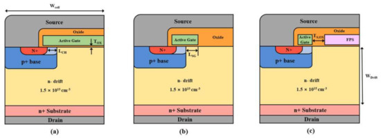
Figure 1.
Schematic cross-sectional views of the MOSFETs. (a) C-DMOSFET (conventional planar DMOSFET); (b) SG-DMOSFET (split-gate DMOSFET); (c) FPS-DMOSFET (floating p+ polysilicon DMOSFET).
The present study proposes and analyzes a new SG-DMOSFET with floating p+ polysilicon (FPS-DMOSFET) in comparison with a conventional planar MOSFET (C-DMOSFET) and conventional SG-DMOSFET through technology computer-aided design Technology Computer-Aided Design (TCAD) simulations. The floating p+ polysilicon (FPS) of the FPS-DMOSFET forms an accumulation layer in the on state and disperses the high drain voltage due to the relatively low potential in the off state. Consequently, the FPS-DMOSFET can have a shorter LSG with significantly less BFOM degradation than the SG-DMOSFET. In addition, it can overcome the problem of electric-field crowding at the active gate oxide, enabling stable operation. The simulation results show that the FPS-DMOSFET achieves not only the best HF-FOM among the studied structures but also an EMOX lower than 3 MV/cm.
2. Device Structures and Fabrication Process
The simulations in this study were conducted using Sentaurus TCAD simulation from Synopsys, Inc. [12]. The models used in the simulation include the doping-dependent carrier mobility model; Shockley–Read–Hall (SRH) recombination, Auger recombination, and inversion and accumulation layer mobility models, and de Man models for impact ionization. Incomplete ionization, high-field velocity saturation, and band-narrowing models are also used [13,14,15].
2.1. Device Concept and Key Parameters
Figure 1 shows schematic cross-sectional views of (a) a C-DMOSFET, (b) a SG-DMOSFET, and (c) the proposed FPS-DMOSFET. The doping concentration and device dimensions of the C-DMOSFET and SG-DMOSFET are described in our previous work [10]. All structures had a drift-layer thickness of 30 μm and an n-drift doping concentration of 1.5 × 1015 cm−3. The channel length was 0.5 μm, the doping concentration of the channel region was 1 × 1017 cm−3, and a fixed charge concentration of 3 × 1012 cm−2 was included at the interface between 4H-SiC and SiO2 to set an adequate threshold voltage. In addition, the LSG of the SG-DMOSFET was 0.7 μm. The detailed device parameters are listed in Table 1. In the FPS-DMOSFET, FPS is inserted between the active gates. It plays a role in preventing the deterioration of the static characteristics because FPS disperses the high drain voltage in the off state and forms an accumulation layer in the on state, resulting in superior BFOM compared to the SG-DMOSFET.

Table 1.
Device parameters of the three devices.
2.2. Proposed Fabrication Process
Figure 2 shows the proposed fabrication procedure of the FPS-DMOSFET. First, the p+ base and n+ source regions are formed by ion implantation. Next, thermal oxidation and n+ polysilicon deposition are performed, as shown in Figure 2b. Then, n+ polysilicon is etched using reactive-ion etching (RIE) to form a split active gate. Subsequently, an interlayer dielectric oxide (ILD) is deposited through low-pressure chemical vapor deposition (LPCVD), which forms a relatively low defect density [16,17]. Next, the ILD is etched to form space for FPS. The thickness of the side oxide between the active gate and FPS (TS,OX) is one of the most important parameters in FPS-DMOSFETs, which affects both static and dynamic characteristics. Therefore, in this ILD etching process, TS,OX is determined by the alignment of the ILD etching process. Accordingly, the oxide between the FPS and n-drift is formed with a thickness of 50 nm through thermal oxidation. Next, p+ polysilicon is deposited by LPCVD and etch-back [18,19]. ILD is deposited through LPCVD again. Finally, the source and drain electrodes are formed.
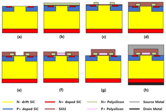
Figure 2.
Proposed fabrication procedure of FPS-DMOSFET (floating p+ polysilicon DMOSFET). (a) form the p+ base and n+ source region; (b) thermal oxidation and n+ polysilicon deposition; (c) n+ polysilicon etching; (d) ILD (interlayer dielectric oxide) oxide deposition; (e) oxide etching and oxidation; (f) p+ polysilicon deposition and etch back; (g) ILD oxide deposition and etching; (h) form the source and drain electrode.
3. Results and Discussion
3.1. FPS-DMOSFET Optimization
In the FPS-DMOSFET optimization process, LSG is one of the most important parameters that determine the performance. A decrease in LSG leads to a decrease in CGD, which improves the HF-FOM; however, it causes deterioration of static characteristics such as BV and RON,SP. Therefore, LSG should be optimized to enhance the performance of the proposed FPS-DMOSFET, considering both BFOM and HF-FOM.
Figure 3 shows the change rate of RON,SP, BV, and CGD according to LSG. To simultaneously analyze the effect of LSG on device characteristics, the RON,SP, BV, and CGD of the FPS-DMOSFET were compared by dividing them by the corresponding values for the C-DMOSFET. First, as shown in Figure 3, the FPS-DMOSFET does not increase RON,SP even if LSG decreases, unlike the SG-DMOSFET, because the FPS forms an accumulation layer in the on state. This allows the FPS-MOSFET to significantly improve the trade-off relationship between BFOM and HF-FOM. On the other hand, a decrease in LSG affects BV and CGD. Figure 3 shows that a reduction of LSG slightly decreases BV while causing a significant improvement in CGD. Therefore, considering both BFOM and HF-FOM, the best performance of the FPS-DMOSFET can be obtained when LSG is set to 0 μm. Although it is difficult to achieve precise alignment in the fabrication process, we assumed it to be the ideal case in the simulation. In addition, as the FPS-DMOSFET is proposed for high-frequency applications, optimization has been performed with a focus on reducing CGD.
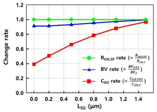
Figure 3.
Change rate of CGD, RON,SP and BV (gate-to-drain capacitance, specific on resistance and breakdown voltage) compared to C-DMOSFET (conventional planar DMOSFET) when TS,OX (thickness of the side oxide) is 250 nm.
However, the FPS-DMOSFET has a higher CGD than the SG-DMOSFET when they have the same LSG. Figure 4 shows the CGD change of the SG-DMOSFET and FPS-DMOSFET according to the change in LSG. In Figure 4, the CGD of the FPS-DMOSFET is larger than that of the SG-DMOSFET when both have the same LSG because of the FPS between the active gates in the FPS-DMOSFET. Figure 5 shows the capacitance analysis of the two structures and a capacitance model that schematically shows these capacitances. The CGD of the SG-DMOSFET consists of a series connection of (1) Cox, the capacitance formed by the overlapping region between the active gate and n-drift and (2) CDEP, the capacitance formed by the depletion region in the junction field effect transistor (JFET) region [9]. Therefore, the CGD of the SG-DMOSFET can be expressed as follows:

Figure 4.
Comparison of CGD (gate-to-drain capacitance) values of SG-DMOSFET (split-gate DMOSFET) and FPS-DMOSFET (floating p+ polysilicon split-gate DMOSFET) according to LSG (active gate length) change.
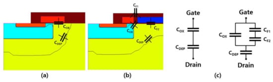
Figure 5.
Depletion lines and CGD (gate-to-drain capacitance) factors distribution of (a) SG-DMOSFET (split-gate DMSOFET); (b) FPS-DMOSFET (floating p+ polysilicon split-gate DMOSFET); and (c) models schematically showing the capacitance of the two structures.
In contrast, the CGD of the FPS-DMOSFET has additional capacitance factors originating from the FPS, active gate, and n-drift, as shown in Figure 5b [20]. Therefore, the total CGD of the FPS-DMOSFET can be expressed as follows:
where CF is the total capacitance of the additional factors due to the FPS of the FPS-DMOSFET. In Equation (3), CF1 is the capacitance formed by the overlapping region between the active gate and FPS, and CF2 is the capacitance formed by the overlapping region between the n-drift and FPS. In other words, CF1 is determined by the side-oxide thickness between the active gate and FPS (TS,OX), and CF2 is determined by the gate-oxide thickness (TOX). Based on Equation (2), CF must be minimized to reduce the CGD of the FPS-DMOSFET. However, there is a limit to the increase in TOX because it has a significant influence on the static characteristics. Therefore, the FPS-DMOSFET was optimized by increasing TS,OX to reduce CF.
Figure 6 shows the CGD change of the FPS-DMOSFET according to variations in LSG and TS,OX. The straight lines of each color show the CGD of the SG-DMOSFET, which has a different LSG. The total CGD of the FPS-DMOSFET decreases with increasing TS,OX and then gradually saturates to a similar level to that of SG-DMOSFET. This result is consistent with the capacitance model of FPS-DMOSFET established in Figure 5. Therefore, TS,OX must be increased to minimize CF. However, increasing TS,OX decreases BV because the drain–voltage dispersion effect of the FPS is reduced in the off state. Therefore, TS,OX should be optimized to enhance the performance of the FPS-DMOSFET. In Figure 6, CGD begins to gradually saturate to a level similar to that of SG-DMOSFET for all LSG values from the point where TS,OX is 250 nm. Therefore, the optimized TS,OX of the FPS-DMOSFET is set to 250 nm.
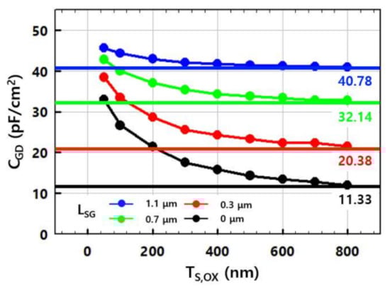
Figure 6.
Comparison of CGD (gate-to-drain capacitance) values of SG-DMOSFET (split-gate DMOSFET) and FPS-DMOSFET (floating p+ polysilicon split-gate DMOSFET) according to LSG (active gate length) change.
3.2. Static Characterisitics
Figure 7 shows the static characteristics, such as BV, RON,SP of the three structures. These results are summarized in Table 2. The on-state characteristics were obtained with VGS and VDS set to 20 V. The C-DMOSFET and FPS-DMOSFET have the same RON,SP of 15.66 mΩ∙cm2, but the SG-DMOSFET has a higher RON,SP of 17.88 mΩ∙cm2. All three structures have the same structure, except for the gate structure. This implies that only the gate structure affects RON,SP. This can be explained through the following equations representing the accumulation-layer resistance (RA,SP) and JFET resistance (RJFET,SP), respectively [21]:
where KA is a coefficient accounting for the current spreading from the accumulation layer to the JFET region, WCELL is the cell pitch, μnA is the electron mobility of the accumulation layer, VGS is the biased gate voltage, and VTH is the threshold voltage. In Equation (5), ρJFET is the conductivity of the JFET region, and W0 is the zero-bias depletion width formed by the junction between the p-base and n-drift under the gate. According to the above equations, a shorter LSG results in a shorter accumulation-layer length, implying a decrease in RA,SP. However, this causes a larger increase in RJFET,SP and a resultant increase in RON,SP. In addition, in the off state (Figure 7b), the leakage current of the FPS-DMOSFET is the largest and the C-DMOSFET is the smallest. This is because the voltage applied to the body diode composed of p+ base and n−drift increases as the active gate length decreases. However, since the leakage currents of the three structures are almost the same, the overall characteristics are not significantly affected.
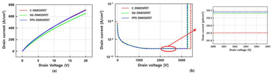
Figure 7.
Static characteristics of the three structures. (a) output curve in the on state and (b) off state leakage current.
Table 2.
Static characteristics of three structures.
Figure 8 shows the electron current densities of the three structures with VGS and VDS set to 20 V. In Figure 8a, the accumulation layer is formed on the entire JFET region owing to the active gate of the C-DMOSFET. On the other hand, in Figure 8b, the accumulation layer breaks in the middle of the JFET because no active gate exists in the middle of the JFET region. As previously mentioned, it leads to an increase in RON,SP due to the increase in RJFET,SP. Therefore, the SG-DMOSFET, which has a shorter LSG, has a 14% larger RON,SP compared with the C-DMOSFET. However, as shown in Figure 8c, the FPS-DMOSFET shows the same transformation of the accumulation layer as the C-DMOSFET, despite having a smaller LSG than those of the C-DMOSFET and SG-DMOSFET. This is because FPS, which has a high electrostatic potential, forms an accumulation layer over the entire JFET region. In addition, Figure 9 shows the electrostatic potential of the three structures with VGS and VDS set to 20 V. Figure 9b shows that the SG-DMOSFET has a remarkably low electrostatic potential in the region where the active gate does not exist. However, as shown in Figure 9c, the electrostatic potential of the FPS is very close to that of the active gate; therefore, the FPS-DMOSFET shows a similar performance as the C-DMOSFET in the on state. In the off state, the p+ base junction is the main region that sustains the high drain voltage before avalanche breakdown. Furthermore, this cause of breakdown is strengthened as LSG decreases, leading to premature p+ base junction breakdown [22]. This is the main cause of the BFOM deterioration in the SG-DMOSFET. Figure 10 shows the electrostatic potential in the off state (VDS = 3000 V, VGS = 0 V). Unlike the SG-DMOSFET (Figure 10b), the FPS-DMOSFET in Figure 10c maintains a relatively low electrostatic potential at the center of the gate structure owing to the FPS. In other words, in the FPS-DMOSFET, the FPS mitigates this effect. Consequently, the concentrated drain voltage across the p + base junction is distributed. Therefore, the optimized FPS-DMOSFET has a BV very close to that of the SG-DMOSFET, although the LSG (=0 μm) is significantly lower than that of the SG-DMOSFET (0.7 μm).
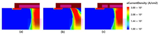
Figure 8.
Electron current density of (a) C-DMOSFET (conventional planar DMOSFET); (b) SG-DMOSFET (split-gate DMOSFET); and (c) FPS-DMOSFET (floating p+ polysilicon DMOSFET) in the on state (VGS = 20 V, VDS = 20 V).
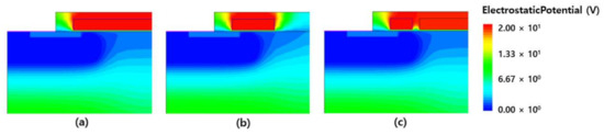
Figure 9.
Electron current density of (a) C-DMOSFET (conventional planar DMOSFET); (b) SG-DMOSFET (split-gate DMOSFET); and (c) FPS-DMOSFET (floating p+ polysilicon DMOSFET) in the on state (VGS = 20 V, VDS = 20 V).
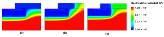
Figure 10.
Electrostatic potential of (a) C-DMOSFET (conventional DMOSFET); (b) SG-DMOSFET (split-gate DMOSFET); and (c) FPS-DMOSFET (floating p+ polysilicon DMOSFET) in the off state (VDS = 3000 V, VGS = 0 V).
Moreover, owing to the relatively low electrostatic potential of the FPS, the FPS-DMOSFET has a smaller EMOX than the SG-DMOSFET. Figure 11 shows the electric-field distribution of the three structures with VDS and VGS set to 3000 V and 0 V, respectively. The SG-DMOSFET shows an EMOX of 3.4 MV/cm owing to the electric-field crowding effect at the active gate corner. Consequently, the SG-DMOSFET does not guarantee the reliability of the gate oxide. On the other hand, the EMOX of C-DMOSFET and FPS-DMOSFET is equal to 2.1 MV/cm. Therefore, the FPS-DMOSFET can guarantee gate-oxide reliability with the split-gate structure applied through FPS.

Figure 11.
Electric field distribution of (a) C-DMOSFET (conventional planar DMOSFET); (b) SG-DMOSFET (split-gate DMOSFET); and (c) FPS-DMOSFET (floating p+ polysilicon DMOSFET) in the off state (VDS = 3000 V, VGS = 0 V).
3.3. Dynamic Characteristics
In the simulation of dynamic characteristics, the active area of the device under test (DUT) was set to 1 cm2. Figure 12a,b show the capacitance graphs of the three structures. The capacitance simulation conditions were as follows: the AC small signal was set to 1 MHz, VGS was fixed at 0 V, and VDS was swept from 0 V to 1500 V. Figure 12a indicates that the FPS-DMOSFET exhibits the smallest CGD. As mentioned earlier for the capacitance modeling, the FPS-DMOSFET has additional CGD factors due to the FPS. However, the optimized FPS-DMOSFET has a smaller LSG than the SG-DMOSFET, resulting in a smaller CGD. In addition, because TS,OX is sufficiently thick (=250 nm), additional CGD factors due to the FPS are significantly eliminated. Similar to CGD, the input capacitance (CISS) is a very important parameter because it affects the delay time in the switching cycle [23]. As shown in Figure 12b, the CISS values of the FPS-DMOSFET, SG-DMOSFET, and C-DMOSFET are 10.13, 11.82, and 12.37 nF/cm2, respectively. This is because the gate–source capacitance (CGS) decreases as LSG decreases. Moreover, in Figure 12b, all three structures have almost the same output capacitance (COSS).
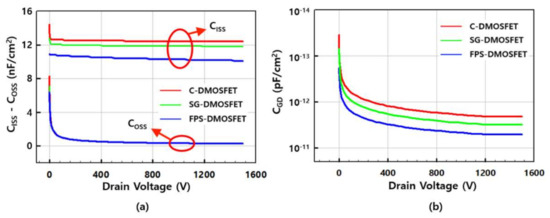
Figure 12.
Capacitance curves of three structures extracted through simulation. (a) CGD curve; (b) CISS and COSS curves.
Figure 13a shows the gate charges of the three structures. The test circuit is shown in Figure 13b, and a constant current of 100 mA was used to charge the gate. In addition, a supply voltage of 1700 V and a load current of 100 A were used to charge the gate of the test circuit. The total gate charge (QG) affects the delay time, and it is dependent on CISS. Moreover, QGD determines the switching power loss and it is dependent on CGD. The extracted QGD values for the C-DMOSFET, SG-DMOSFET, and FPS-DMOSFET are 240.2, 131.1, and 102.8 nC/cm2, respectively, while the extracted QG values are 894.1, 545.0, and 419.3 nC/cm2, respectively.
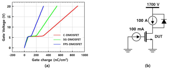
Figure 13.
(a) Gate Charge curves of three structures and (b) the test circuit for gate charge simulation.
Finally, switching parameters such as the turn-on time (TON), turn-off time (TOFF), turn-on energy loss (EON), and turn-off energy loss (EOFF) are extracted through a double-pulse test simulation, and the results are summarized in Table 3. Figure 14a,b show the turn-off and turn-on transients of the double-pulse test simulation. In addition, the test circuit for the double-pulse test simulation is shown in Figure 14c. In this circuit, the external gate resistance and stray inductance were set to 10 Ω and 10 nH, respectively. The gate voltage was swept from −5 V to 20 V to switch between the off and on states. The supply voltage and load inductance were set to 1700 V and 170 μH, respectively, and the first gate pulse was biased for 10 μs; therefore, the load current was set to 100 A/cm2. The body diode of the DUT was used as a freewheeling diode.
Table 3.
Dynamic characteristics of three structures.
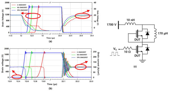
Figure 14.
The switching waveforms of three structures extracted by double pulse test simulation. (a) drain voltage and gate voltage waveforms; (b) drain voltage and drain current waveforms; and (c) the test circuit for double pulse test simulation.
In this paper, TON and TOFF are defined as follows [24]:
where TD,ON is the turn-on delay (from 10% of VGS to 90% of VDS at the rising edge of the second pulse), TR is the rise time in the turn-on transient (from 90% to 10% of VDS at the rising edge of the second pulse), TD,OFF is the turn-off delay (from 90% of VGS to 10% of VDS at the falling edge of the first pulse), and TF is the fall time in the turn-off transient (from 10% to 90% of VDS). As a result, FPS-DMOSFET with CISS has the fastest TON and TOFF as 71.1 ns and 310.9 ns, respectively.
In addition, Figure 15 shows the extracted total switching energy loss (ETOTAL = EON + EOFF) of the three structures. Due to the smallest CGD, FPS-DMOSFET has the EON of 3.31 mJ/cm2 and EOFF of 5.20 mJ/cm2, so that ETOTAL is 8.51 mJ/cm2, which decrease by 43% and 21%, respectively, compared to C-DMOSFET and SG-DMOSFET.
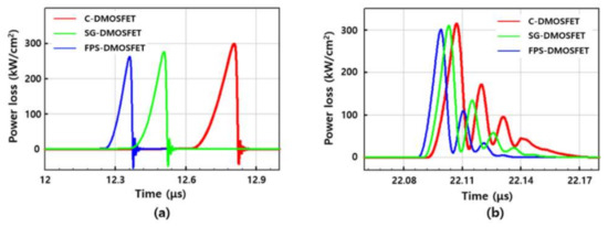
Figure 15.
The switching power loss of three structures extracted by double pulse test. (a) turn off transient and (b) turn on transient.
4. Conclusions
In this paper, an SG-DMOSFET with floating p+ polysilicon (FPS-DMOSFET) was proposed and analyzed in comparison with a C-DMOSFET and a SG-DMOSFET through TCAD simulations. The FPS-DMOSFET shows a shorter LSG with significantly less BFOM degradation than the SG-DMOSFET because the proposed structure has FPS between the active gates, forming an accumulation layer in the on state and dispersing the high drain voltage due to the relatively low potential in the off state. As a result, the HF-FOM of the FPS-DMOSFET is improved by 61% and 49%, respectively, compared to the C-DMOSFET and SG-DMOSFET. Therefore, the FPS-DMOSFET not only has the fastest TON and TOFF, but also the smallest EON and EOFF during the switching operation. Moreover, the FPS-DMOSFET has an EMOX of 2.1 MV/cm, which is lower than that of the SG-DMOSFET (3.4 MV/cm) and the same as that of C-DMOSFET. This implies that the FPS-DMOSFET can guarantee reliable operation. Therefore, FPS-DMOSFETs can significantly improve HF-FOM while solving serious problems in SG-DMOSFETs, such as BFOM degradation and a high EMOX at high voltages.
Author Contributions
Conceptualization, K.C.; data curation, J.Y.; writing-original draft, K.C. and J.Y.; writing- review and editing, K.K. All authors have read and agreed to the published version of the manuscript.
Funding
This research received no external funding.
Acknowledgments
This research was supported by the MSIT (Ministry of Science and ICT), Korea, under the ITRC (Information Technology Research Center) support program (IITP-2021-2018-0-01421) supervised by the IITP (Institute for Information & Communications Technology Planning & Evaluation).
Conflicts of Interest
The authors declare no conflict of interest.
References
- Cooper, J.A.; Agarwal, A. SiC power-switching devices—The second electronics revolution? Proc. IEEE 2002, 90, 956–968. [Google Scholar] [CrossRef]
- Ji, S.; Zhang, Z.; Wang, F. Overview of high voltage sic power semiconductor devices: Development and application. CES Trans. Electr. Mach. Syst. 2017, 1, 254–264. [Google Scholar] [CrossRef]
- Yang, T.; Wang, Y.; Yue, R. SiC Trench MOSFET with Reduced Switching Loss and Increased Short-Circuit Capability. IEEE Trans. Electron Devices 2020, 67, 3685–3690. [Google Scholar] [CrossRef]
- Jiang, H.; Wei, J.; Dai, X.; Ke, M.; Deviny, I.; Mawby, P. SiC Trench MOSFET With Shielded Fin-Shaped Gate to Reduce Oxide Field and Switching Loss. IEEE Electron Device Lett. 2016, 37, 1324–1327. [Google Scholar] [CrossRef]
- Ni, W.; Wang, X.; Xu, M.; Wanga, Q.; Feng, C.; Xiao, H.; Lijuan, J.; Wei, L. Study of Asymmetric Cell Structure Tilt Implanted 4H-SiC Trench MOSFET. IEEE Electron Device Lett. 2019, 40, 698–701. [Google Scholar] [CrossRef]
- Krishnaswami, S.; Das, M.; Hull, B.; Ryu, S.H.; Scofield, J.; Agarwal, A.; Palmour, J. Gate oxide reliability of 4H-SiC MOS devices. In Proceedings of the 43rd Annual, 2005 International Reliability Physics Symposium on IEEE, San Jose, CA, USA, 17–21 April 2005. [Google Scholar]
- Hamada, K.; Hino, S.; Kitani, T. Low On-Resistance SiC-MOSFET with a 3.3-kV Blocking Voltage. Mitsubishi Electr. Adv. 2015, 149, 14–17. [Google Scholar]
- Baliga, B.J. Power semiconductor device figure of merit for high-frequency applications. IEEE Electron Device Lett. 1989, 10, 455–457. [Google Scholar] [CrossRef]
- Han, K.; Baliga, B.J.; Sung, W. Split-Gate 1.2-kV 4H-SiC MOSFET: Analysis and Experimental Validation. IEEE Electron Device Lett. 2017, 38, 1437–1440. [Google Scholar] [CrossRef]
- Shuming, X.; Changhong, R.Y.; Liang, C.; Foo, J.K.P.; Sin, O. Theoretical analysis and experimental characterization of the dummy-gated VDMOSFET. IEEE Trans. Electron Devices 2001, 48, 2168–2176. [Google Scholar] [CrossRef]
- Cha, K.Y.; Yoon, J.W.; Cheon, J.H.; Kim, K.S. The limitation of the Split-Gate MOSFET(SG-MOSFET) at 3.3 kV. In Proceedings of the 2021 International Conference on Electronics, Information, and Communication (ICEIC), Jeju, Korea, 31 January–3 February 2021; pp. 655–658. [Google Scholar]
- Synopsys Inc. Sentaurus Device Manual, User Manual, Version O-2018.06; Synopsys Inc.: Mountain View, CA, USA, 2006. [Google Scholar]
- Darwish, M.N.; Lentz, J.L.; Pinto, M.R.; Zeitzoff, P.M.; Krutsick, T.J.; Vuong, H.H. An improved electron and hole mobility model for general purpose device simulation. IEEE Trans. Electron Devices 1997, 44, 1529–1538. [Google Scholar] [CrossRef]
- Van Overstraeten, R.; De Man, H. Measurement of the ionization rates in diffused silicon p-n junctions. Solid State Electron 1970, 13, 583–608. [Google Scholar] [CrossRef]
- Mujtaba, S.A. Advanced Mobility Models for Design and Simulation of Deep Submicrometer MOSFETs. Ph.D. Thesis, Stanford University, CA, 1995. [Google Scholar]
- Rao, V.R.; Eisele, I.; Patrikar, R.M.; Sharma, D.K.; Vasi, J.; Grabolla, T. High-field stressing of LPCVD gate oxides. IEEE Electron Device Lett. 1997, 18, 84–86. [Google Scholar]
- Ahn, J.; Ting, W.; Kwong, D.L. Comparison of performance and reliability between MOSFETs with LPCVD gate oxide and thermal gate oxide. IEEE Trans. Electron Devices 1997, 38, 2709–2710. [Google Scholar] [CrossRef]
- Bashir, R.; Hebert, F. PLATOP: A novel planarized trench isolation and field oxide formation using poly-silicon. IEEE Electron Device Lett. 1996, 17, 352–354. [Google Scholar] [CrossRef]
- Saxena, R.S.; Kumar, M.J. Dual-Material-Gate Technique for Enhanced Transconductance and Breakdown Voltage of Trench Power MOSFETs. IEEE Trans. Electron Devices 2009, 56, 517–522. [Google Scholar] [CrossRef]
- Hossain, N.M.; Chowdhury, M.H. Multilayer Graphene Nanoribbon and Carbon Nanotube based Floating Gate Transistor for Nonvolatile Flash Memory. Acm J. Emerg. Technol. Comput. Syst. 2015, 12, 1–17. [Google Scholar] [CrossRef]
- Baliga, B.J. DMOSFET Structures Advanced Power MOSFET Concept; Springer Science + Business Media, LLC: New York, NY, USA, 2010; pp. 25–31. [Google Scholar]
- Han, Z.; Song, G.; Bai, Y.; Chen, H.; Liu, X.; Lu, J. A novel 4H-SiC MOSFET for low switching loss and high-reliability applications. Semicond. Sci. Technol. 2020, 35, 1–9. [Google Scholar] [CrossRef]
- Baliga, B.J. Power MOSFETs Fundamentals of Power Semiconductor Devices; Springer International Publishing AG, Part of Natrure: New York, NY, USA, 2019; pp. 441–449. [Google Scholar]
- Graovac, D.; Purschel, M.; Kiep, A. MOSFET power losses calculation using the data-sheet parameters application note, v1.1. Infineon Technol. AG 2006, 1, 1–23. [Google Scholar]
Publisher’s Note: MDPI stays neutral with regard to jurisdictional claims in published maps and institutional affiliations. |
© 2021 by the authors. Licensee MDPI, Basel, Switzerland. This article is an open access article distributed under the terms and conditions of the Creative Commons Attribution (CC BY) license (http://creativecommons.org/licenses/by/4.0/).