Article

Area-Time Efficient Two-Dimensional Reconfigurable Integer DCT Architecture for HEVC

1
Sandhaan Labs Private Limited, Bhubaneswar 751016, Odisha, India
2
School of Computer Science and Engineering, Nanyang Technological University, Singapore 639798, Singapore
3
Department of Electronic Engineering, Myongji University, Yongin 17058, Korea
*
Author to whom correspondence should be addressed.
Electronics 2021, 10(5), 603; https://doi.org/10.3390/electronics10050603
Submission received: 26 January 2021 / Revised: 19 February 2021 / Accepted: 26 February 2021 / Published: 5 March 2021
(This article belongs to the Special Issue System-on-Chip (SoC) Design and Its Applications)

Abstract

:
In this paper, we present area-time efficient reconfigurable architectures for the implementation of the integer discrete cosine transform (DCT), which supports all the transform lengths to be used in High Efficiency Video Coding (HEVC). We propose three 1D reconfigurable architectures that can be configured for the computation of the DCT of any of the prescribed lengths such as 4, 8, 16, and 32. It is shown that matrix multiplication schemes involving fewer adders can be used to derive parallel architectures for 1D integer DCT of different lengths. A novel transposition buffer is designed to be used for the proposed 2D DCT architecture, which offers double the throughput without increasing the size of the transposition buffer. We determine the optimal pipeline locations in the proposed design through the precise estimation of propagation delays and the critical path so that the area-delay-product is optimized and all the output samples are obtained in the same cycle in spite of the recursive nature of the structure. Implementation results show that the proposed 2D integer DCT architectures provide significantly higher throughput per unit area than the existing designs for HEVC.

1. Introduction

The discrete cosine transform (DCT) is a core operation in video compression due to its near-optimal de-correlation efficiency [1,2]. The Joint Collaborative Team-Video Coding (JCT-VC) has defined the integer DCTs for transform lengths, N = 4 , 8, 16, and 32 for the video coding standard H.265/HEVC (High Efficiency Video Coding) [3,4]. Low-cost hardware implementations of the integer DCTs for HEVC were proposed in [5,6,7,8,9,10,11,12,13].
Ahmed et al. [8] proposed a multiplier-less lifting-based approach applied to a sparse decomposition of the DCT matrices. Shen et al. [14] proposed another multiplier-less implementation using a multiple constant multiplication (MCM) approach for the integer DCT of lengths four and eight. For the DCT of lengths 16 and 32, however, they used conventional multipliers. Park et al. [9] used Chen’s factorization of the DCT where the butterfly operation of the DCT computation was implemented by the processing element (PE) with only shifters, adders, and multiplexors. Budagavi and Sze [10] proposed a unified hardware structure that can be used for forward, as well as inverse DCTs. Efficient MCM-based architectures and transposition buffers for integer DCT for HEVC were proposed in [12,13]. However, the transposition unit has a significant overhead of complexity in this design.
As a major deviation from the earlier video coding standards, HEVC allows DCTs of four different lengths. The DCT unit for HEVC is therefore required to be configurable to support different transform lengths, N = 4 , 8, 16, and 32. Based on this requirement, in this paper, we propose efficient reconfigurable structures of the DCT unit that can be used for integer DCTs of different lengths. Specifically, three reconfigurable DCT architectures based on a constant matrix multiplication (CMM) and the MCM are proposed. 2D integer DCT architectures having novel transposition buffers are also proposed. The innovations of the proposed architectures are summarized as follows.
  • A hardware-oriented algorithm for integer DCT computation for HEVC is proposed.
  • Three different flexible hardware architectures for the integer DCT are proposed, each with advantages in terms of area, delay, or power.
  • A novel matrix-vector-product unit that involves fewer adders than the existing method [12,13] is proposed.
  • A novel 2D integer DCT architecture having double the throughput and less latency (without increasing the size of the transposition buffer) is proposed.
  • A novel low-cost pipeline strategy is proposed to reduce the critical path of the proposed 1D integer DCT.
  • Comparisons with existing methods are provided in terms of various metrics such as gate counts, maximum usable frequency, throughput, latency, etc.
The rest of the paper is organized as follows. In the next section, we discuss the key features of the integer DCT for HEVC. We describe three proposed reconfigurable architectures of 1D integer DCT in Section 3. In Section 4, we discuss the implementation of 2D DCT. In Section 5, we compare the area and time complexities of the proposed designs with those of the existing designs. Section 6 presents the conclusions.

2. Key Features of Integer DCT for HEVC

The N-point integer DCT of an input vector x = [ x ( 0 ) , x ( 1 ) , , x ( N 1 ) ] is given by:
y ( 0 ) y ( 1 ) · · · y ( N 2 ) y ( N 1 ) = C N x ( 0 ) x ( 1 ) · · · x ( N 2 ) x ( N 1 )
where the integer DCT kernel C N is an N × N matrix of integers and y = [ y ( 0 ) , y ( 1 ) , , y ( N 1 ) ] is an output vector. The kernel matrices C N for N = 4 , 8, 16, and 32 for HEVC were defined by JCT-VC [3]. The N-point integer DCT for HEVC can be computed by a partial butterfly approach using an ( N / 2 ) -point DCT and a product of the ( N / 2 ) × ( N / 2 ) matrix by an ( N / 2 ) -point vector as:
y ( 0 ) y ( 2 ) · · · y ( N 4 ) y ( N 2 ) = C N / 2 a ( 0 ) a ( 1 ) · · · a ( N / 2 2 ) a ( N / 2 1 )
and
y ( 1 ) y ( 3 ) · · · y ( N 3 ) y ( N 1 ) = S N / 2 b ( 0 ) b ( 1 ) · · · b ( N / 2 2 ) b ( N / 2 1 )
where:
a ( i ) = x ( i ) + x ( N i 1 )
b ( i ) = x ( i ) x ( N i 1 ) ,
for i = 0 , 1 , · · · , N / 2 1 . C N / 2 is an ( N / 2 ) -point integer DCT kernel of size ( N / 2 ) × ( N / 2 ) . S N / 2 is also an integer matrix of size ( N / 2 ) × ( N / 2 ) derived from the first N / 2 columns of the odd-indexed rows of C N , such that the ( i , j ) th entry of S N / 2 can be defined as:
s N / 2 i , j = c N 2 i + 1 , j for 0 i , j N / 2 1
where c N 2 i + 1 , j is the ( 2 i + 1 , j ) th entry of C N . Note that all even DCT outputs are given by Equation (2a), while odd DCT outputs are given by Equation (2b). An ( N / 2 ) -point DCT given by Equation (2a) is again decomposed into an ( N / 4 ) -point DCT and a product of the integer matrix S N / 4 of size ( N / 4 ) × ( N / 4 ) with an ( N / 4 ) -point vector. This decomposition can continue recursively till the N-point DCT is expressed in terms of the four-point DCT and a product of the 4 × 4 matrix and four-point vector.

3. Proposed Reconfigurable Architectures for 1D Integer DCT

In this section, we propose three reconfigurable architectures for the computation of the 1D integer DCT of different lengths for HEVC.

3.1. Proposed 1D DCT Architecture-1

Figure 1 shows the proposed 1D DCT Architecture-1. The architecture in Figure 1a is for the integer DCTs of lengths N = 8 , 16, and 32, whereas the architecture in Figure 1b is for the computation of the four-point integer DCT. Figure 1c describes the structure of the shift-add unit in Figure 1b. Sixteen- or eight- or four-point integer DCTs can be computed by the 32-point DCT structure by setting the s e l control signal to the MUX unit appropriately. The input adder unit (IAU) in Figure 1a computes a ( i ) and b ( i ) for i = 0 , 1 , · · · , N / 2 1 by Equation (3). The MUX unit, which consists of N / 2 2:1 MUXes, selects either a ( i ) or x ( i ) for i = 0 , 1 , · · · , N / 2 1 , depending on whether it is used to compute Equation (2a) or the DCT of a lower size, respectively. Odd-indexed coefficients of y ( i ) for i = 1 , 3 , · · · , N 1 are computed by the matrix-vector-product unit (MVPU) according to Equation (2b). The computation of Equation (2b) could be realized as a CMM problem [15,16,17,18]. We find that the algorithm of Boullis and Tisserand [18] is very efficient when it is used for the computation of the MVPU. We generated the MVPU algorithm for S 4 · b 4 , S 8 · b 8 , and S 16 · b 16 and list these in Table 1, where b N / 2 = [ b ( 0 ) , b ( 1 ) , · · · b ( N / 2 1 ) ] . The complexity of the proposed 1D DCT Architecture-1 is compared to that in [12] in Table 2 since the DCT computation in [12] also uses a partial butterfly approach based on Equations (2a) and (2b). Table 1 of [12] shows the algorithm of the reference DCT architecture to be compared. Specifically, the IAUs of the two structures are the same, and the MVPU of the proposed structure corresponds to the MCM of [12]. The total number of adders listed in the seventh column of Table 2 can be referred to Table 2 of [12]. The proposed Architecture-1 uses 14.6 % fewer adders compared with [12] for N = 32 . Note that pipeline registers are not used for the implementation of the MVPU. The structure requires only input registers after the IAU to hold the incoming data.
Adding pipeline registers in the critical path is the general practice in VLSI design. However, in the recursive design as in the proposed DCT, the locations of pipeline registers need to be carefully decided. Furthermore, the pipelining in the MVPU may significantly increase the silicon area. We could find optimal pipeline locations through precise estimation of propagation delays in the critical path so that area-delay-product can be optimized and all the output samples can be obtained in the same cycle even in the recursive structure. Architecture-1 for the eight-point DCT involves four pipeline registers before the MVPU to reduce the propagation delay, as shown in Figure 1a. In order to obtain all eight DCT coefficients in the same cycle, four more registers are inserted after the first four adders in the four-point integer DCT unit, as shown in Figure 1b. Similarly, eight and 16 registers are located before the MVPU for 16- and 32-point DCTs, respectively. Note that Architecture-1 involves two pipeline stages for any of the DCT sizes, N = 4 , 8, 16, and 32. The array of AND gates is used to disable the IAU, pipeline registers, and MVPU in the computation of the DCT of a lower size in order to reduce the power consumption.

3.2. Proposed 1D DCT Architecture-2

The proposed Architecture-2 is an extension of Architecture-1, as shown in Figure 2, which incorporates coarse-grained reconfiguration with additional hardware units to maintain the same throughput rate for all the transform lengths. It uses an extra ( N / 2 ) -point architecture over the structure of Figure 1a, which takes the input [ x ( N / 2 ) ,..., x ( N 1 ) ] . The output of this additional ( N / 2 ) -point architecture is multiplexed with the output of the MVPU by MUX Unit-2. The 32-point architecture can compute one 32-point DCT, two 16-point DCTs, four 8-point DCTs, and eight 4-point DCTs, while the throughput remains the same as the 32 DCT coefficients per cycle irrespective of the desired transform size.

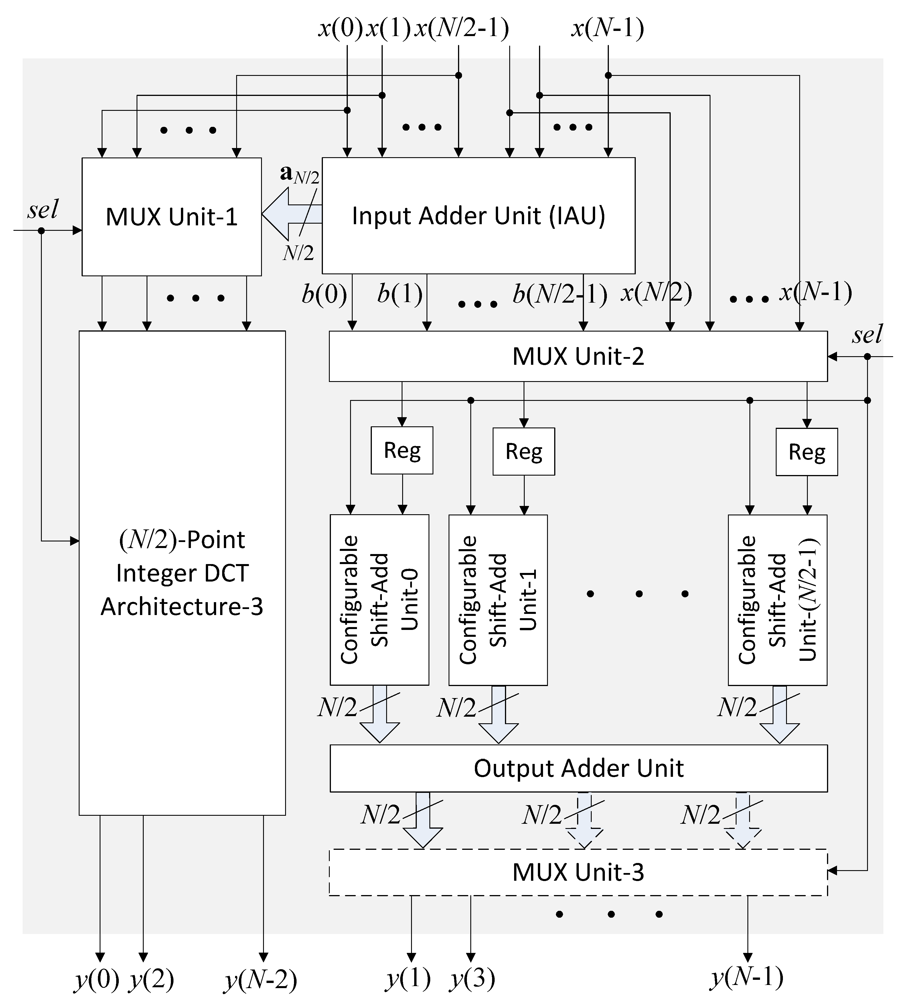
3.3. Proposed 1D DCT Architecture-3

Figure 3 shows the proposed Architecture-3 for 1D DCT. It incorporates a fine-grained reconfiguration for different transform lengths. For the computation of the N-point DCT, the ( N / 2 ) -point integer DCT unit computes Equation (2a), whereas the configurable shift-add units (CSAU) and the output adder unit (OAU) perform the computation of (2b). In order to reuse this architecture for the computation of the ( N / 2 ) -point DCT, the ( N / 2 ) -point integer DCT unit computes an ( N / 2 ) -point DCT, and the CSAU and OAU compute the other ( N / 2 ) -point DCT providing two ( N / 2 ) -point DCTs. Similarly, for the computation of the ( N / 4 ) -point DCT, the ( N / 2 ) -point DCT unit computes two ( N / 4 ) -point DCTs, and the CSAU and OAU compute the other two ( N / 4 ) -point DCTs, producing four ( N / 4 ) -point DCTs. Figure 4a shows the structure of CSAU-1, which is one out of four CSAUs used for the eight-point DCT structure. For the computation of the four-point DCT, CSAU-1 multiplies x ( 5 ) with [ 64 , 36 , 64 , 83 ] in the second column of C 4 (ignoring the signs of the coefficients). This is part of the four-point DCT computation of [ x ( 4 ) , x ( 5 ) , x ( 6 ) , x ( 7 ) ] . For the computation of the eight-point DCT, CSAU-1 multiplies b ( 1 ) with [ 75 , 18 , 89 , 50 ] , which is the second column of S 4 . As shown in Figure 4a, the CSAU can be designed based on the SAU with several MUXes; however, it does not need any additional adder. Each CSAU is designed differently so that the last four MUXes have different combinations of coefficients corresponding to the desired configuration. Since the signs of the coefficients in each configuration may also be different, the OAU is implemented using add/subunits instead of adders or subtractors, as shown in Figure 4b. When the 16-point DCT structure is to be used for the computation of the four-point DCT, the intermediate results of Stage-2 in the three-stage adder-tree in the OAU are directed to the output y ( i ) , unlike the computation for eight- and 16-point DCTs. Therefore, the MUX Unit-3, which involves an array of 2:1 MUXes, is used to select the desired outputs of Stage-2 or outputs of Stage-3. Similarly, a MUX Unit-3 consisting of 3:1 MUXes is used to select the desired outputs of Stages-2, 3, and 4 for the 32-point DCT structure. Since MUX Unit-3 is not required for the eight-point DCT structure, it is indicated by dashed lines as shown in Figure 3.

4. High-Throughput 2D Integer DCT Architecture

Figure 5 shows the proposed architecture for 2D integer DCT using N-point reconfigurable 1D integer DCTs. It consists of two sections corresponding to two stages of 2D DCT computation by row-column decomposition based on the separable property of 2D DCT. The input section of the proposed structure consists of two N-point 1D integer DCTs, to compute the 1D DCT of all the N columns of the N × N input matrix. The first N-point DCT unit (S1-A) computes the DCTs of the first ( N / 2 ) columns of the N × N input matrix, while the second N-point DCT unit (S1-B) computes the DCTs of the last ( N / 2 ) columns of the input matrix. A transposition unit consisting of four ( N / 2 ) × ( N / 2 ) buffers is employed to reorder the DCT coefficients of different columns to be fed to the output section row-wise. The output section consists of two 1D parallel N-point DCT units, to compute the 1D DCT of all the N rows of the N × N intermediate output matrix. The first N-point DCT unit (S2-A) computes the DCT of even rows of the intermediate matrix (available from SR_Even_A and SR_Even_B). The second N-point DCT unit (S2-B) computes the DCT of the odd rows in the intermediate matrix (available from SR_Odd_A and SR_Odd_B).
In each cycle, two columns of the N × N input matrix x are fed to the input section of the proposed 2D DCT architecture as inputs. For example, if Column-0 and column- ( N / 2 ) of the input matrix are fed, respectively, to the DCT units S1-A and S1-B in the input section in the current clock cycle, then Column-1 and column- ( N / 2 + 1 ) are fed concurrently to S1-A and S1-B, respectively, in the next clock cycle. Hence, the entire N × N input matrix is fed to the proposed architecture in N / 2 consecutive clock cycles. The first two rows of 2D DCT from the output section are available after ( N / 2 + 2 ) clock cycles where N / 2 clock cycles are for transposition and two clock cycles for the input and output sections.
In every N / 2 cycle, the proposed 2D DCT architecture can process a new N × N input matrix, resulting in a throughput rate of 2 N DCT coefficients per clock cycle. Therefore, the 2D DCT architecture using 32-point Architecture-1 has 8, 16, 32, and 64 coefficients per clock cycle for the 4-, 8-, 16-, and 32-point DCT computations, respectively. Furthermore, the 2D DCT architecture employing 32-point Architecture-2 or 3 can produce 64 DCT coefficients per clock cycle irrespective of the transform size.
The conventional way to obtain double the throughput is to use double the hardware comprised of two DCT units and the transposition buffers. However, the proposed 2D DCT transposition technique does not increase the transposition buffer size to increase the throughput. The 32 × 32 transposition buffer occupies a 2.1 times larger area than the 32-point integer DCT unit; therefore, the savings of the transposition buffer result in the significant savings in the total silicon area.

5. Implementation Results

The proposed 2D architectures using 32-point 1D Architectures-1, -2, and -3 are coded in VHDL and synthesized by Synopsys Design Compiler using the TSMC 90nm CMOS library. Table 3 lists the gate count, maximum usable frequency (MUF), samples/cycle, throughput (TPT), latency, power consumption, and energy per sample (EPS) of the proposed 2D architectures and existing architectures [6,7,11,12,13]. Throughput per second per gate (TSG) (Ksamples/s/gate) is also listed in the last column in Table 3. Architecture-n in Table 3 means 2D architectures based on conventional transposition by a 32 × 32 transposition buffer and two proposed 1D architectures-n. The architecture- n means 2D architectures using four 1D architectures-n and four ( N / 2 ) × ( N / 2 ) transposition buffers as proposed in Section 4. Existing designs [6,7,13] and proposed Architectures-1 and - 1 have different throughputs depending on the transform length. In Table 3, note that the TPT and TSG values of these designs were calculated based on the maximum throughput in the case of the 32-point DCT computation, and we specifically indicated * with the values. Architectures-1 and 2 can have a 400 MHz MUF, whereas the MUF of Architecture-3 is found to be 380 MHz. Architecture- 2 offers the smallest EPS among the proposed and existing architectures, which have a constant throughput. The throughput of Architecture-1 varies with the DCT size; however, Architectures-2 and -3 yield 32 samples in every cycle, resulting in 12.80 and 12.16 giga samples per second (GSPS) for all different DCT sizes. The 32-point architecture- n uses four 16 × 16 transposition buffers, which involves the same area as 32 × 32 transposition buffers used in 32-point architecture-n, but has double the throughput of 64 samples per cycle and half the transposition latency. Therefore, Architectures- 2 and - 3 have 25.60 and 24.33 GSPS for all the transform sizes. The TSGs of the 2D architectures using the proposed Architecture-1 are the best for the computation of the 32-point DCT, but decrease for DCTs of lower sizes. The 2D architectures using 1D Architecture-3 offer better TSGs than those using 1D Architecture-2, but have a lower throughput. Architecture- n provides 1.32 times better TSG than architecture-n on average for 32-point DCT computations of Architectures 1, 2, and 3. The proposed 2D architectures offer higher throughput, as well as lower latencies and, accordingly, higher TSGs than the existing 2D architectures.

6. Summary and Conclusions

In this paper, we propose area-time efficient architectures for 2D integer DCT to be used in HEVC. Three reconfigurable architectures that support the computation of integer DCT of different sizes are proposed. We propose a novel transposition buffer and a 2D DCT architecture, which provides double the throughput and half the transposition latency without increasing the size of the transposition buffer. Implementation results show that the proposed architectures provide more throughput per unit area than the existing integer DCT architectures for HEVC. The DCT is a basic transform that can be used for the implementation of other widely used transforms such as discrete Fourier transform (DFT), discrete Hartley transform (DHT), and discrete sine transform (DST).

Author Contributions

Conceptualization, P.K.M., S.-K.L., T.S., and S.Y.P.; methodology, P.K.M., S.-K.L., and S.Y.P.; validation, S.Y.P. and D.H.K.; writing—original draft preparation, S.-K.L. and S.Y.P.; writing—review and editing, P.K.M., D.H.K., and S.Y.P. All authors read and agreed to the published version of the manuscript.

Funding

This work was supported by the National Research Foundation of Korea (NRF) grant funded by the Korea government (MSIT) (No. 2019R1F1A1060820).

Acknowledgments

The EDA Tool was supported by the IC Design Education Center.

Conflicts of Interest

The authors declare no conflict of interest.

References

  1. Chen, J.; Liu, S.; Deng, G.; Rahardja, S. Hardware Efficient Integer Discrete Cosine Transform for Efficient Image/Video Compression. IEEE Access 2019, 7, 152635–152645. [Google Scholar] [CrossRef]
  2. Ahmed, N.; Natarajan, T.; Rao, K. Discrete cosine transform. IEEE Trans. Comput. 1974, 100, 90–93. [Google Scholar] [CrossRef]
  3. JCTVC-G495, CE10: Core Transform Design for HEVC: Proposal for Current HEVC Transform. Available online: http://phenix.it-sudparis.eu/jct/doc_end_user/current_document.php?id=3752 (accessed on 4 March 2021).
  4. Bross, B.; Han, W.; Ohm, J.; Sullivan, G.; Wang, Y.; Wiegand, T. High Efficiency Video Coding HEVC Text Specification Draft 10, JCTVC-L1003. Available online: http://phenix.int-evry.fr/jct/doc_end_user/documents/8_San%20Jose/wg11/JCTVC-H1003-v22.zip (accessed on 4 March 2021).
  5. Singhadia, A.; Bante, P.; Chakrabarti, I. A Novel Algorithmic Approach for Efficient Realization of 2D-DCT Architecture for HEVC. IEEE Trans. Consum. Electron. 2019, 65, 264–273. [Google Scholar] [CrossRef]
  6. Zhao, W.; Onoye, T.; Song, T. High-Performance Multiplierless Transform Architecture for HEVC. In Proceedings of the IEEE International Symposium on Circuits and Systems, Beijing, China, 19–23 May 2013; pp. 1668–1671. [Google Scholar]
  7. Zhu, J.; Liu, Z.; Wang, D. Fully Pipelined DCT/IDCT/Hadamard Unified Transform Architecture for HEVC Codec. In Proceedings of the IEEE International Symposium on Circuits and Systems, Beijing, China, 19–23 May 2013; pp. 677–680. [Google Scholar]
  8. Ahmed, A.; Shahid, M.U.; ur Rehman, A. N-point DCT VLSI architecture for emerging HEVC standard. VLSI Des. 2012, 2012, 752024. [Google Scholar] [CrossRef] [Green Version]
  9. Park, J.S.; Nam, W.J.; Han, S.M.; Lee, S. 2D large inverse transform (16×16, 32×32) for HEVC (High Efficiency Video Coding). J. Semicond. Technol. Sci. 2012, 12, 203–211. [Google Scholar] [CrossRef]
  10. Budagavi, M.; Sze, V. Unified forward + inverse transform architecture for HEVC. In Proceedings of the IEEE International Conference on Image Processing, Orlando, FL, USA, 30 September–3 October 2012; pp. 209–212. [Google Scholar]
  11. Sun, H.; Zhou, D.; Zhu, J.; Kimura, S.; Goto, S. An area-efficient 4/8/16/32-point inverse DCT architecture for UHDTV HEVC decoder. In Proceedings of the IEEE International Conference on Visual Communications and Image Processing, Valletta, Malta, 7–10 December 2014; pp. 197–200. [Google Scholar]
  12. Meher, P.K.; Park, S.Y.; Mohanty, B.K.; Lim, K.S.; Yeo, C. Efficient Integer DCT Architectures for HEVC. IEEE Trans. Circuits Syst. Video Technol. 2014, 24, 168–178. [Google Scholar] [CrossRef]
  13. Park, S.Y.; Meher, P.K. Flexible integer DCT architectures for HEVC. In Proceedings of the IEEE International Symposium on Circuits and Systems, Beijing, China, 19–23 May 2013; pp. 1376–1379. [Google Scholar]
  14. Shen, S.; Shen, W.; Fan, Y.; Zeng, X. A unified 4/8/16/32-point integer IDCT architecture for multiple video coding standards. In Proceedings of the IEEE International Conference on Multimedia and Expo, Melbourne, VIC, Australia, 9–13 July 2012; pp. 788–793. [Google Scholar]
  15. Software/Hardware Generation of DSP Algorithms. Available online: http://www.spiral.net/ (accessed on 4 March 2021).
  16. Potkonjak, M.; Srivastava, M.B.; Chandrakasan, A.P. Multiple constant multiplications: Efficient and versatile framework and algorithms for exploring common subexpression elimination. IEEE Trans. Comput.-Aided Des. Integr. Circuits Syst. 1996, 15, 151–165. [Google Scholar] [CrossRef]
  17. Macleod, M.D.; Dempster, A.G. Common subexpression elimination algorithm for low-cost multiplierless implementation of matrix multipliers. Electron. Lett. 2004, 40, 651–652. [Google Scholar] [CrossRef]
  18. Boullis, N.; Tisserand, A. Some optimizations of hardware multiplication by constant matrices. IEEE Trans. Comput. 2005, 54, 1271–1282. [Google Scholar] [CrossRef]
Figure 1. (a) Proposed Architecture-1 for N = 8 , 16, and 32. (b) Four-point integer DCT architecture. (c) Shift-add unit used in (b).
Electronics 10 00603 g001
Figure 2. Proposed Architecture-2 for N = 8 , 16, and 32. The four-point integer DCT architecture is same as the one shown in Figure 1b.
Electronics 10 00603 g002
Figure 3. Proposed Architecture-3 for N = 8 , 16, and 32. The number of output samples of the output adder unit (OAU) is N / 2 , N, and 3 N / 2 for N = 8 , 16, and 32, respectively. The four-point integer DCT architecture is the same as the one shown in Figure 1b.
Electronics 10 00603 g003
Figure 4. (a) Configurable Shift-Add Unit (CSAU)-1 for the eight-point DCT structure. (b) The OAU for the eight-point DCT structure. Input of the OAU ( a , b , c ) means the output of CSAU-a where b and c are used for the four- or eight-point DCT computations according to s e l , respectively.
Electronics 10 00603 g004
Figure 5. Proposed architecture for the 2D integer DCT of size N × N .
Electronics 10 00603 g005
Table 1. Computation of S N / 2 · b N / 2 in the matrix-vector-product unit ( b i = b ( i ) and y 2 × i + 1 = y ( 2 × i + 1 ) for i = 0 , 1 , 2 , , N / 2 1 ).
Computation of S 4 · b 4 in the matrix-vector-product unit (MVPU) for 8-point DCT computation
t 9 = b 0 + 4 b 0 ; t 8 = b 1 8 b 3 ; t 7 = 4 b 2 b 2 ; t 6 = 2 b 0 b 3 ; t 5 = 2 b 1 b 3 ; t 4 = b 1 2 b 2 16 b 3 ; t 3 = b 0 2 t 5 ; t 2 = 4 t 7 + 8 b 3 b 2 ; t 1 = 8 b 0 + b 1 + 4 b 1 2 b 0 ;
y 1 = 16 t 1 + t 3 + 16 t 7 t 4 8 b 0 ; y 3 = 16 t 9 8 t 2 2 t 8 t 9 16 b 1 b 2 2 b 3 ; y 5 = 8 t 1 + t 6 + 16 b 2 t 4 64 t 5 4 b 3 ; y 7 = t 2 + 16 t 3 + t 6 + 16 t 8 + 64 b 2 2 b 1 ;
Computation of S 8 · b 8 in the MVPU for 16-point DCT computation
t 21 = b 3 b 6 ; t 20 = b 2 + b 7 ; t 19 = b 0 b 5 ; t 18 = b 0 + b 1 ; t 17 = b 2 b 4 ; t 16 = 4 b 0 + 2 b 5 b 6 ; t 15 = b 0 4 b 2 2 b 4 ; t 14 = 2 b 3 + 4 b 5 b 7 ; t 13 = 2 b 1 4 b 4 + b 5 ;
t 12 = 2 b 0 4 b 1 b 3 ; t 11 = b 4 + 4 b 6 + 2 b 7 ; t 10 = b 1 + 2 b 2 4 b 7 ; t 9 = b 2 + 4 b 3 + 2 b 6 ; t 8 = 16 t 12 + b 0 + 64 b 4 + 8 b 6 8 t 20 ; t 7 = 16 t 11 + 8 t 18 + 64 b 3 + b 7 8 b 5 ;
t 6 = 8 t 18 + 8 b 4 16 t 9 64 b 5 b 6 ; t 5 = 16 t 13 + b 1 8 t 21 64 b 2 8 b 7 ; t 4 = 16 t 16 + 8 t 20 + b 5 64 b 1 8 b 4 ; t 3 = 16 t 10 + 8 t 19 + b 2 + 8 b 3 64 b 6 ;
t 2 = 16 t 14 + 64 b 0 + 8 b 1 + b 3 8 t 17 ; t 1 = 16 t 15 + 8 t 21 + 64 b 7 b 4 8 b 5 ; y 1 = 128 t 18 + 2 b 0 + b 4 t 5 t 6 t 14 32 b 0 b 5 ;
y 3 = t 9 + 128 t 19 + b 1 + b 3 + 32 b 5 t 7 t 8 2 b 5 ; y 5 = t 1 + t 2 + t 10 + b 5 + 2 b 6 128 t 21 32 b 6 b 7 ; y 7 = t 3 + t 4 + b 1 + 2 b 4 t 12 128 t 17 32 b 4 b 7 ;
y 9 = t 4 + b 0 + 2 b 3 + 128 b 3 t 3 t 11 32 b 3 128 b 5 b 6 ; y 11 = t 2 + 32 b 1 + b 2 t 1 t 16 b 0 2 b 1 128 b 1 128 b 4 ;
y 13 = t 8 + t 13 + 128 t 20 + 2 b 2 t 7 32 b 2 b 4 b 6 ; y 15 = t 6 + t 15 + 128 b 6 + 32 b 7 t 5 b 2 b 3 2 b 7 128 b 7 ;
Computation of S 16 · b 16 in the MVPU for 32-point DCT computation
t 108 = b 8 + b 14 ; t 107 = b 0 b 10 ; t 106 = b 12 8 b 15 ; t 105 = b 8 b 13 ; t 104 = b 9 b 15 ; t 103 = b 2 16 b 8 ; t 102 = 2 b 0 + b 5 ; t 101 = b 0 2 b 14 ; t 100 = b 5 b 7 ;
t 99 = 8 b 7 + b 11 ; t 98 = 2 b 7 b 10 ; t 97 = 32 b 5 b 13 ; t 96 = b 8 2 b 9 ; t 95 = b 3 8 b 9 ; t 94 = b 10 + 32 b 13 ; t 93 = b 6 + 8 b 11 ; t 92 = 2 b 8 b 14 ; t 91 = b 8 + b 9 ;
t 90 = b 4 + 2 b 12 ; t 89 = b 4 32 b 8 ; t 88 = 4 b 4 b 10 ; t 87 = b 1 + 2 b 3 ; t 86 = b 13 + b 15 ; t 85 = b 1 2 b 4 ; t 84 = 2 b 1 b 8 ; t 83 = 4 b 5 b 8 ; t 82 = b 5 8 b 14 ;
t 81 = 2 b 11 + b 12 ; t 80 = 8 b 6 b 13 ; t 79 = b 1 + b 7 ; t 78 = b 2 + 2 b 10 ; t 77 = b 8 16 b 9 ; t 76 = b 14 + 2 b 15 ; t 75 = b 6 b 8 ; t 74 = b 1 + b 15 ; t 73 = b 11 8 b 14 ;
t 72 = 16 b 6 + b 7 ; t 71 = 2 b 6 b 15 ; t 70 = 2 b 1 b 11 ; t 69 = b 3 + 2 b 4 ; t 68 = b 0 b 6 ; t 67 = b 6 2 b 7 ; t 66 = b 2 + b 7 ; t 65 = b 7 8 b 9 ; t 64 = b 0 b 12 ;
t 63 = b 4 2 b 12 ; t 62 = 16 b 2 b 5 ; t 61 = b 6 b 7 ; t 60 = 2 b 11 b 12 ; t 59 = 4 b 1 b 3 ; t 58 = 8 b 3 b 7 ; t 57 = b 0 + b 14 ; t 56 = b 0 + 4 b 13 ; t 55 = 2 b 0 + b 14 ;
t 54 = t 57 2 b 9 ; t 53 = t 91 + 2 b 2 ; t 52 = t 55 + 2 b 12 ; t 51 = 2 t 70 + b 9 ; t 50 = t 87 + 4 b 6 ; t 49 = t 61 2 b 13 ; t 48 = b 6 2 b 11 b 13 ; t 47 = b 2 + 2 b 4 + b 9 ;
t 46 = 4 b 4 t 90 ; t 45 = t 74 + 2 b 10 ; t 44 = 2 b 3 + b 14 b 5 ; t 43 = b 1 + b 10 2 b 12 ; t 42 = t 99 + 4 b 11 ; t 41 = t 103 8 b 6 ; t 40 = 4 b 3 t 69 2 b 11 ;
t 39 = 2 b 3 + b 11 2 t 81 ; t 38 = 16 b 3 + 2 b 4 t 67 ; t 37 = 2 t 63 t 60 ; t 36 = 2 b 2 + 4 b 5 + 2 b 13 b 5 ; t 35 = 4 b 2 + 2 b 5 + 2 b 10 b 2 ; t 34 = 2 t 78 b 10 2 b 13 ;
t 33 = 2 b 5 + 4 b 13 2 b 10 b 13 ; t 32 = 8 b 2 + 64 b 9 b 10 16 b 13 ; t 31 = t 62 8 t 80 ; t 30 = b 3 + 4 b 9 + 2 b 15 b 14 ; t 29 = 16 b 7 + 64 b 12 + b 15 8 b 8 ;
t 28 = t 56 + 4 t 84 8 b 6 ; t 27 = 4 t 66 + 8 b 9 + 8 b 14 b 15 ; t 26 = 4 t 75 + b 1 + 8 b 4 + 8 b 12 ; t 25 = t 58 + 4 b 4 + 4 b 9 4 b 7 ; t 24 = 4 t 85 + 4 b 0 + b 9 8 b 3 ;
t 23 = 4 t 107 t 65 8 b 1 ; t 22 = t 93 + 4 b 14 8 b 12 4 b 15 ; t 21 = 4 t 71 + t 83 8 b 14 ; t 20 = t 77 + 32 t 85 + 8 b 0 8 t 76 ; t 19 = t 72 + 16 t 101 + 8 b 15 8 b 1 64 b 11 ;
t 18 = 8 t 98 + 16 t 102 + 8 b 15 64 b 1 b 13 ; t 17 = 8 t 82 + 8 b 0 + 16 b 10 t 103 32 b 15 ; t 16 = 4 t 46 + 2 t 86 + 64 b 0 t 94 b 3 8 b 3 32 b 7 ;
t 15 = 4 t 40 + t 78 + 32 t 98 2 b 8 b 11 32 b 15 ; t 14 = 4 t 37 + 2 t 100 + 32 b 0 + b 4 t 97 64 b 8 ; t 13 = 4 t 36 + 32 t 74 + 2 t 104 + 64 b 6 t 105 ;
t 12 = 4 t 39 + t 102 + 2 t 103 32 b 2 b 12 64 b 15 ;    t 11 = 4 t 33 + 32 t 91 + t 107 + 64 b 1 2 t 108 ; t 10 = 4 t 34 + 32 t 54 + t 66 2 t 68 ;
t 9 = 4 t 35 + 32 t 61 + 2 t 79 + b 5 + 64 b 14 b 15 ; t 8 = 2 t 52 + 2 t 88 + t 95 + 8 b 13 32 t 33 16 t 85 2 t 89 ; t 7 = 2 t 38 + t 73 + 64 b 0 + 2 b 2 + 8 b 3 + 8 b 10 32 t 34 2 t 95 ;
t 6 = 32 t 36 + 2 t 51 + t 63 + 2 t 80 + 8 t 106 + 4 b 8 + 32 b 12 8 b 5 ; t 5 = 32 t 35 + 8 t 42 + 2 t 50 + 4 b 15 t 81 2 t 82 8 b 2 ;
t 4 = 32 t 37 + 2 t 49 + 4 t 52 + 16 t 83 + t 85 8 b 6 32 b 6 ; t 3 = 2 t 45 + 32 t 46 + 16 t 56 + b 9 4 t 38 2 t 59 32 b 1 ;
t 2 = 32 t 39 + 2 t 54 + 4 t 62 + t 93 + 2 t 106 8 t 108 32 b 14 ; t 1 = 2 t 53 + 4 t 87 32 t 40 2 t 99 8 t 104 32 b 9 64 b 10 b 14 ;
y 1 = t 5 + 2 t 11 + t 49 + t 69 + 4 t 72 + t 108 + 128 b 0 + 32 b 12 8 t 24 2 t 24 ; y 3 = t 2 + 2 t 16 + 4 t 41 + t 84 2 t 23 8 t 23 t 47 t 86 128 b 10 ;
y 5 = 2 t 31 + 64 t 55 + 4 b 1 + 2 b 12 t 4 t 15 t 18 t 30 64 t 105 ; y 7 = t 8 + 2 t 20 + 2 t 48 + 64 t 64 + t 64 + 128 b 9 t 9 t 41 8 t 58 4 b 3 ;
y 9 = t 7 + t 13 + t 19 + t 102 + 128 b 14 16 t 25 2 t 43 t 89 4 b 11 ; y 11 = t 16 + 2 t 17 + 8 t 65 + b 4 + 64 b 5 + 4 b 6 + 2 b 7 t 2 t 31 t 51 128 b 8 ;
y 13 = t 4 + 8 t 27 + 2 t 27 + t 44 + b 0 + 64 b 0 + 4 b 5 + b 10 2 t 15 t 96 32 b 1 128 b 2 ; y 15 = t 7 + 2 t 26 + 8 t 26 + t 90 + 64 t 92 + 2 t 102 + t 104 2 t 13 t 57 32 b 11 ;
y 17 = 2 t 10 + 8 t 25 + 2 t 30 + 16 t 42 + t 68 + t 73 t 6 t 45 16 t 59 ; y 19 = 2 t 14 + t 71 + 4 t 94 t 1 8 t 28 2 t 28 t 43 32 t 76 t 100 ;
y 21 = 2 t 18 + t 32 + 64 t 67 + b 6 + b 11 t 3 t 12 4 t 92 2 t 96 2 b 4 64 b 10 ; y 23 = t 6 + t 10 + t 20 + b 11 2 t 29 2 t 44 64 t 70 64 t 75 t 88 ;
y 25 = t 5 + 2 t 19 + t 29 + 2 t 47 + 4 b 12 t 11 64 t 71 t 95 64 b 3 b 13 ; y 27 = t 1 + t 14 + 2 t 32 + 64 t 66 t 17 t 50 2 t 101 64 b 1 b 12 128 b 15 ;
y 29 = t 3 + 8 t 21 + 2 t 21 + t 48 + t 101 + b 2 2 t 12 4 t 97 b 7 64 b 7 32 b 9 ; y 31 = t 8 + 2 t 9 + 4 t 77 2 t 22 8 t 22 t 53 t 60 t 79 32 b 3 128 b 15 ;
Table 2. Complexity comparison in terms of the number of adders. IAU, input adder unit.
NIAUMVPU N / 2 -DCTTotal
[12]Figure 1[12]Figure 1[12]Figure 1
441014
882833145055
16161201125055186183
3232464367186183682582
Table 3. Comparison of different 2D integer DCT architectures.
DesignTech.
(nm)
Gates
(K)
MUF
(MHz)
Samples/
Cycle
TPT
(GSPS)
LatencyPower
(mW)
EPS
(mW × ns)
TSG
(KSPSPG)
Zhao et al. [6]4520533332 4.54  *38 22.09  *
Zhu et al. [7]90412311 4 / 8 / 16 / 32 9.95  * 10 / 14 / 22 / 38 30.50 3.06 24.13  *
Meher et al. [12]9046331032 9.92 32 86.27 8.69 21.41
Sun et al. [11]901553124 1.24 8.04
Park et al. [13]90402336 4 / 8 / 16 / 32 10.77  * 4 / 8 / 16 / 32 69.05 6.40 26.77  *
Architecture-190310400 4 / 8 / 16 / 32 12.80  * 6 / 10 / 18 / 34 39.15 3.05 41.20  *
Architecture-29042340032 12.80 6 / 10 / 18 / 34 68.07 5.31 30.26
Architecture-39036738032 12.16 6 / 10 / 18 / 34 71.65 5.88 33.08
Architecture- 1 90453400 8 / 16 / 32 / 64 25.60  * 4 / 6 / 10 / 18 74.82 2.92 56.43  *
Architecture- 2 9066240064 25.60 4 / 6 / 10 / 18 127.62 4.98 38.66
Architecture- 3 9056138064 24.33 4 / 6 / 10 / 18 138.23 5.68 43.34
MUF: maximum usable frequency. TPT: throughput. EPS: energy per sample. TSG: TPT per second per gate. KSPSPG: Ksamples/s/gate. For designs where the throughput varies with the transform length, the maximum throughput is shown in the TPT and TSG columns, with an * next to the value.
Publisher’s Note: MDPI stays neutral with regard to jurisdictional claims in published maps and institutional affiliations.

