
Research on EDAC Schemes for Memory in Space Applications

 ,
,
Abstract
:1. Introduction
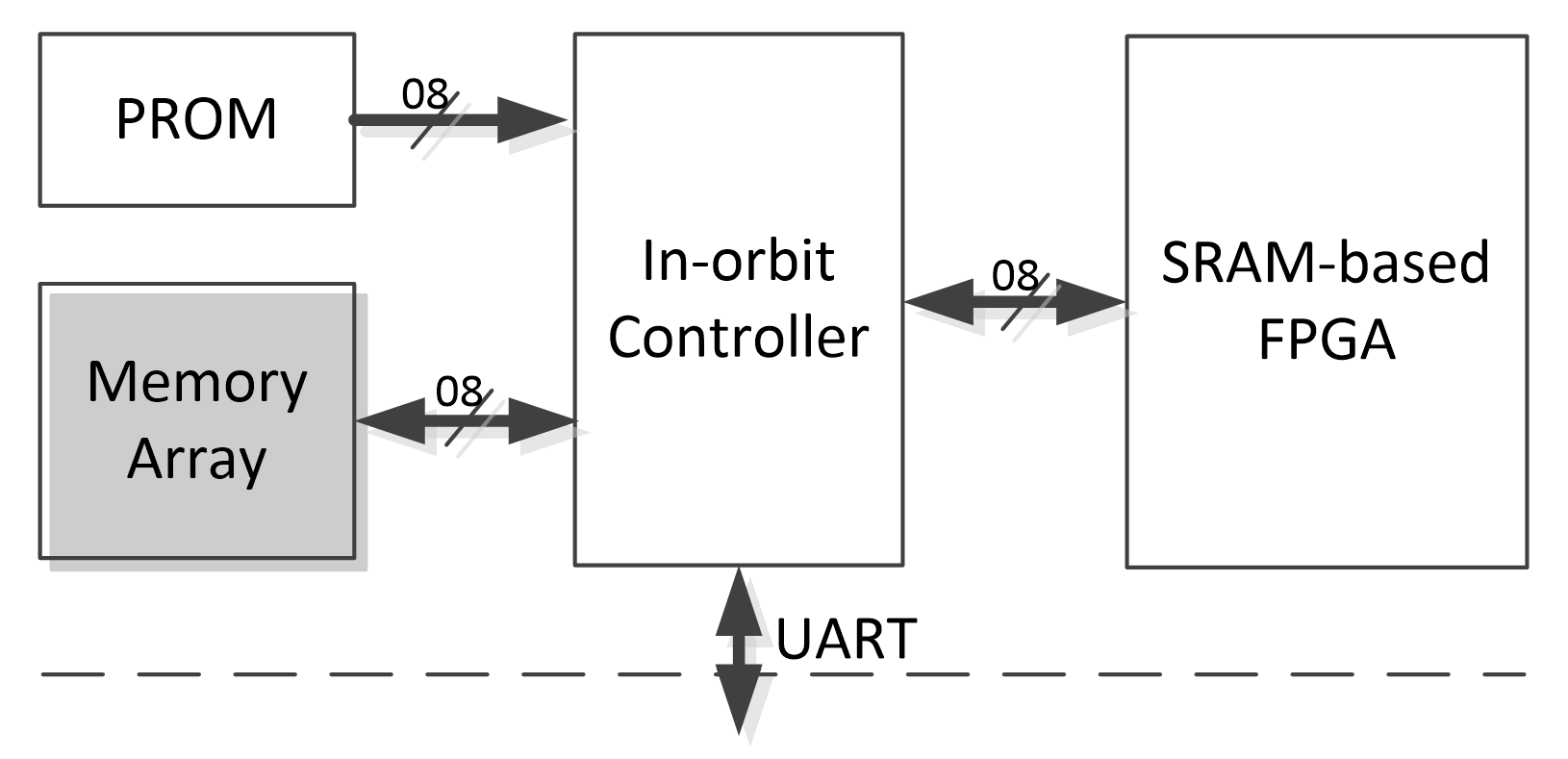
- (1)
- Data encoding: The configuration data are received through the UART, and then redundant encoding is performed by EDAC method.
- (2)
- Periodic readback checking: Check the data stored in the memory array periodically through the FPGA readback function.
- (3)
- Periodic scrubbing: According to the scrub interval set in advance, the memory array can be rewritten unconditionally by continuous scrubbing.
2. Present State-of-the-Art EDAC Schemes
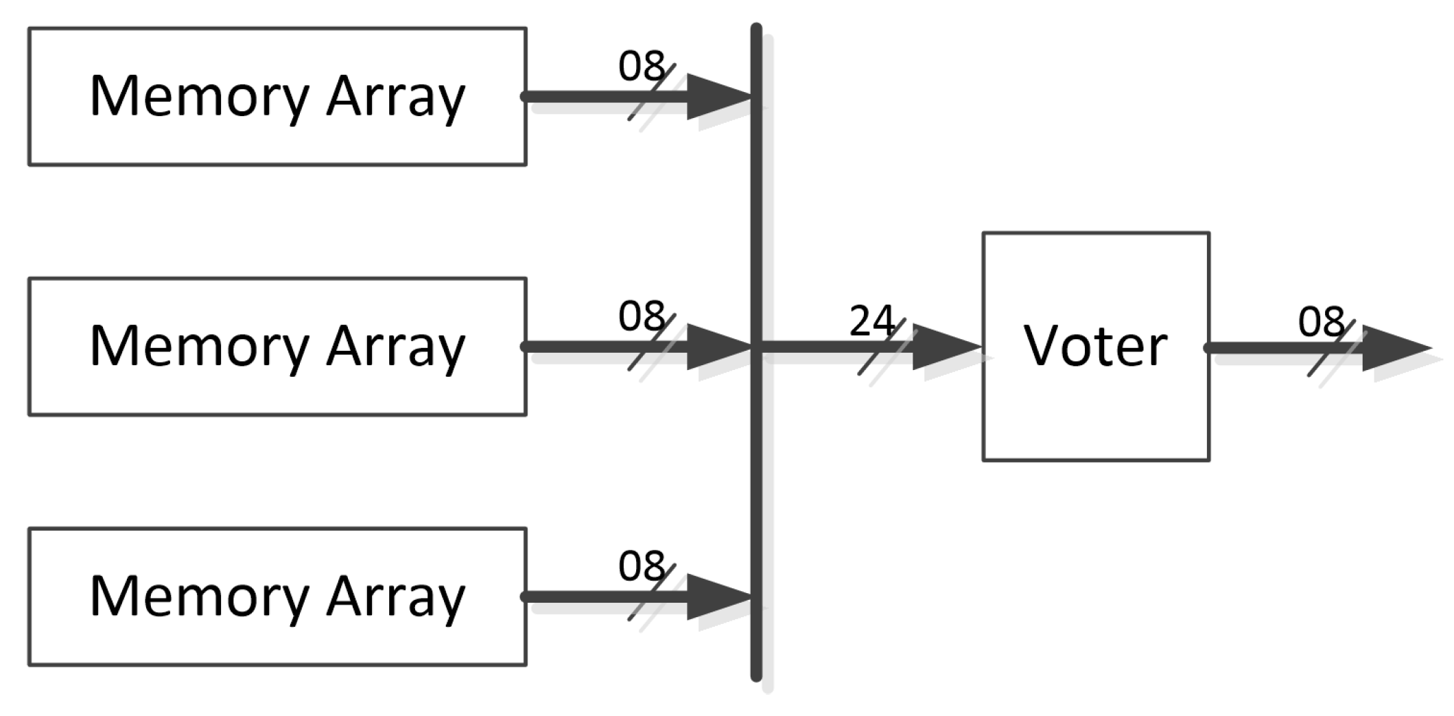
2.1. TMR
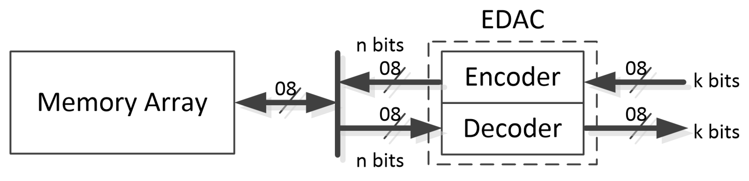
2.2. Linear Block Code Schemes
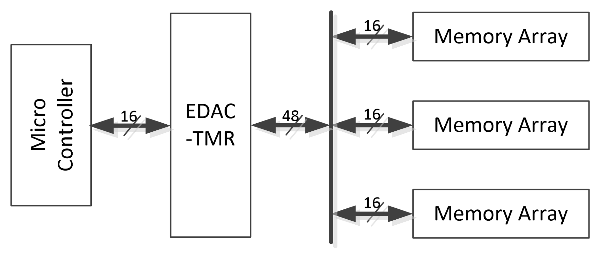
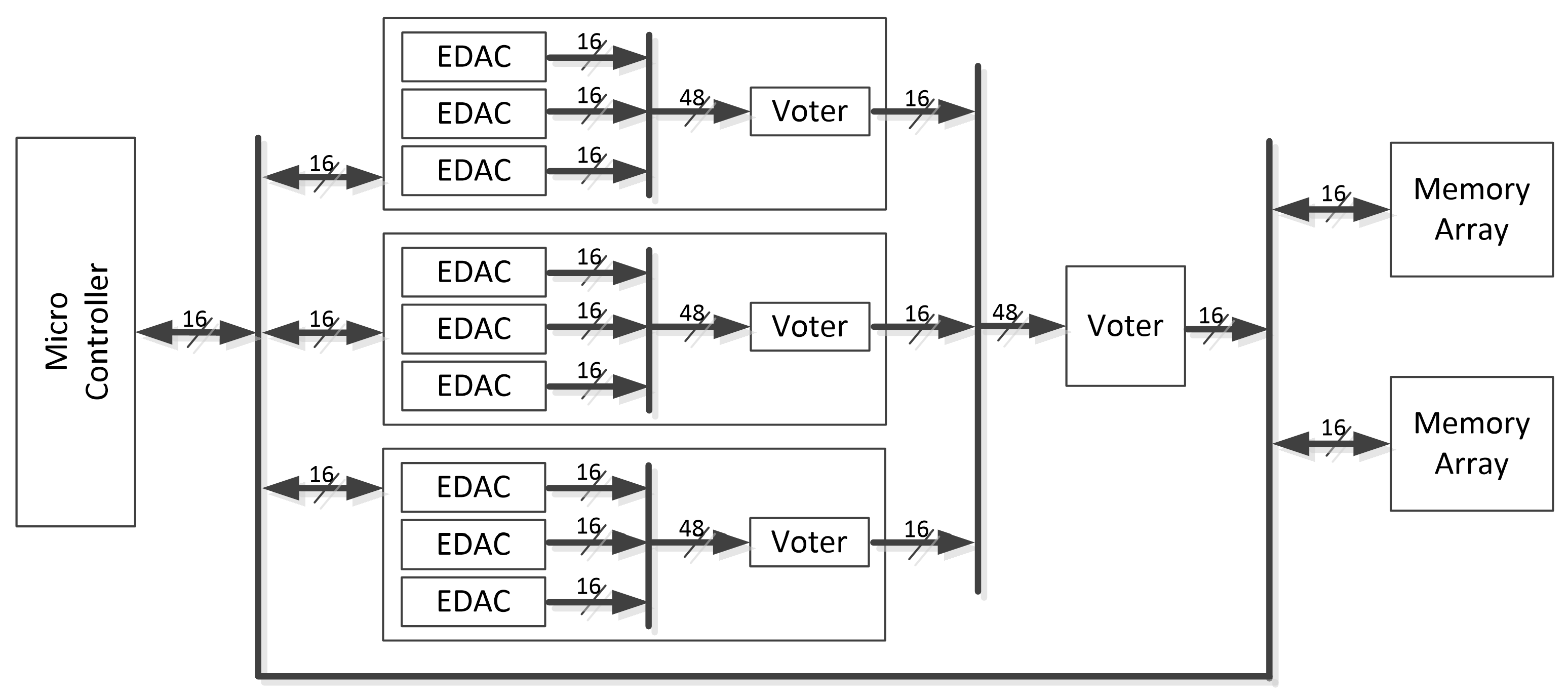
2.3. TMR Based EDAC
2.4. Memory Scrubbing
3. A New Proposed EDAC Scheme
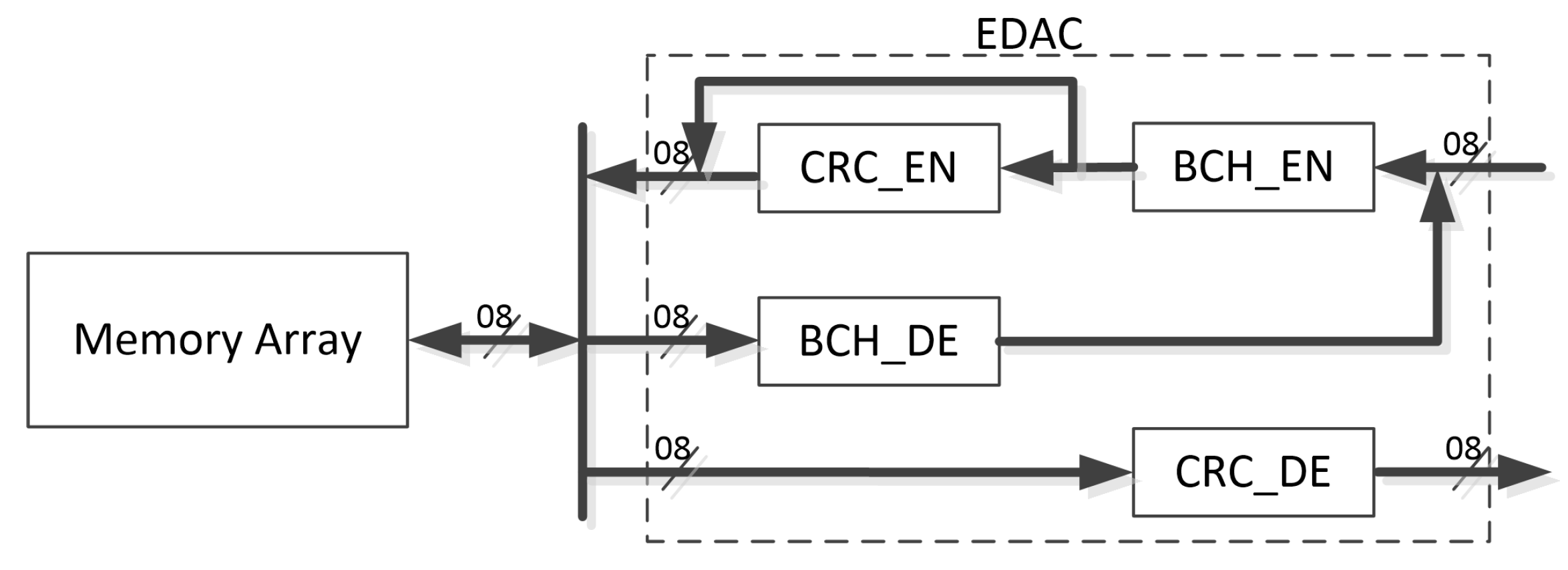
3.1. Cascaded Code Scheme
3.2. BCH
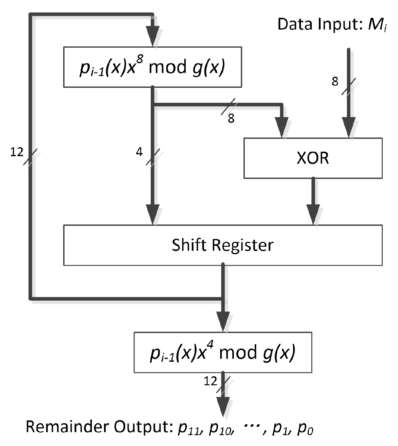
3.2.1. Encoding
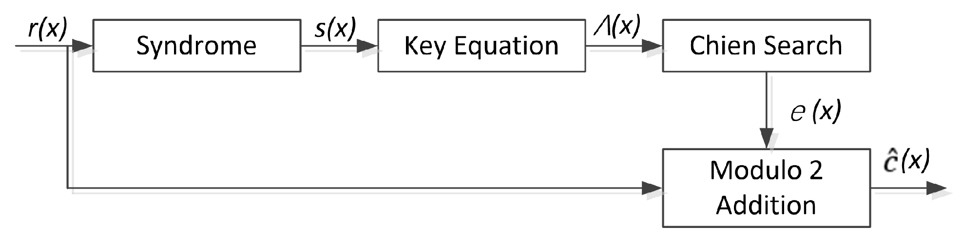
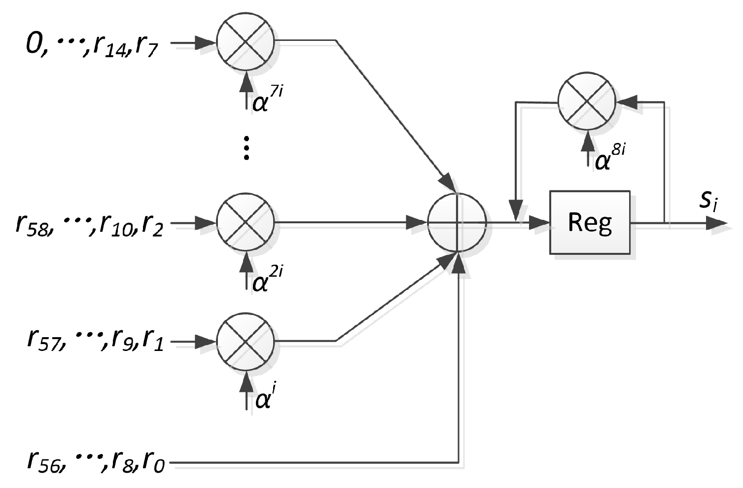
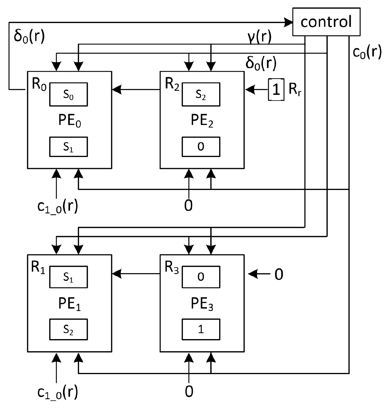
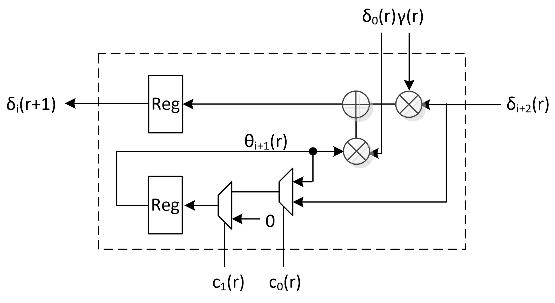
3.2.2. Decoding
- (1)
- Computing the syndrome polynomial based on the input to the decoder.
- (2)
- Calculating the error location polynomial by the key equation.
- (3)
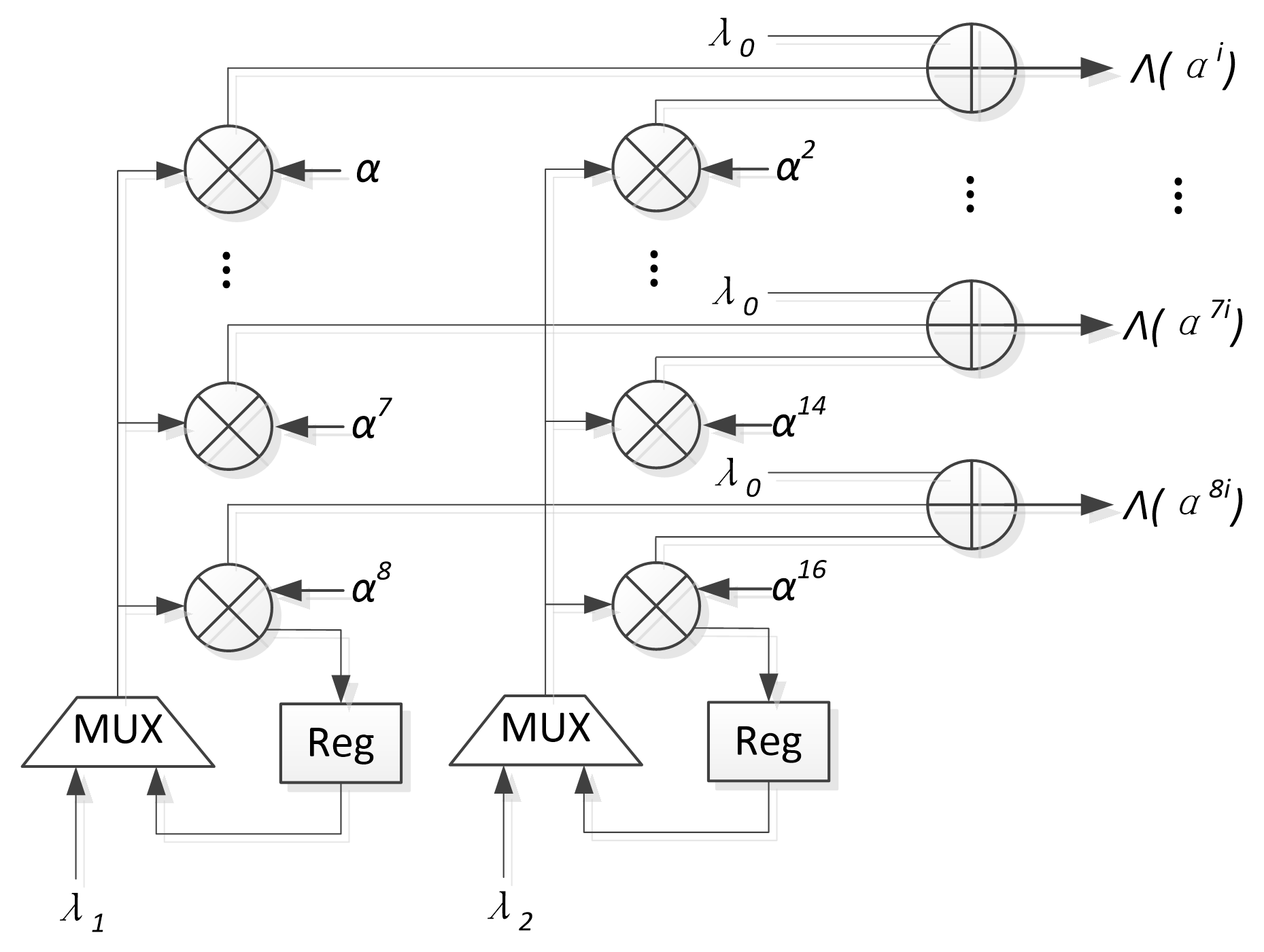
- Calculating the roots () of by Chien search algorithm, and correcting errors based on the roots:
3.3. CRC
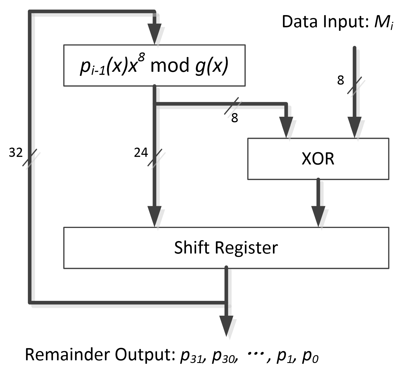
3.3.1. Encoding
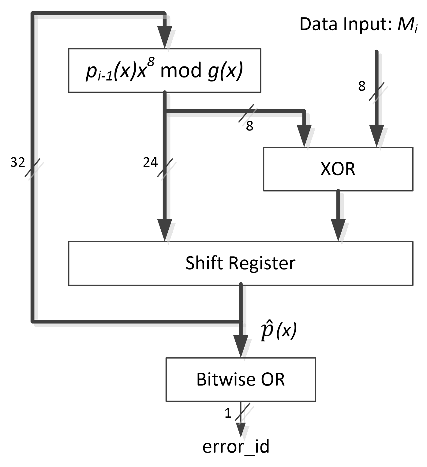
3.3.2. Decoding
3.4. Proposed EDAC Process
- No errors: Both the BCH_DE and the CRC_DE indicate that there are no errors.
- Single-bit or double-bit errors: If the decoding result of the BCH_DE is wrong, the decoded 51 bits data are encoded again by the BCH_EN and written to the blank area of the memory array. Using new encoded data and the old CRC redundant bits, the CRC_DE can identify whether the error has been corrected by the BCH_DE. If yes, overwrite the original data in the memory array with the new encoded data. Otherwise, it means that there are multiple-bit errors and the corresponding memory address should be marked.
- Multiple-bit errors: Other than the above multiple-bit errors, if the decoding result of the BCH_DE is right and the decoding result of the CRC_DE is wrong, it also means that there are multiple-bit errors and the corresponding memory address should be marked.
4. Experimental Results
5. Conclusions
Author Contributions
Funding
Data Availability Statement
Conflicts of Interest
References
- Bentoutou, Y.; Mohammed, A.S. A Review of in-orbit Observations of Radiation-Induced Effects in Commercial Memories on board ALSAT-1. World Acad. Sci. Eng. Technol. J. 2012, 6, 652–654. [Google Scholar]
- Yoshinaga, T.; Watanabe, M. Optically Reconfigurable Gate Array with a Triple Modular Redundancy. In Proceedings of the 2019 6th International Conference on Space Science and Communication (IconSpace), Johor Bahru, Malaysia, 28–30 July 2019; pp. 276–279. [Google Scholar]
- Guo, C.; Xu, J.; Jiang, S.; An, Y.; Yue, L. A Novel Universal Radiation-hardened FFT Chip Design. In Proceedings of the 2018 International Conference on Radiation Effects of Electronic Devices (ICREED), Harbin, China, 7–11 May 2018; pp. 1–4. [Google Scholar]
- Bentoutou, Y. Program Memories Error Detection and Correction On-Board Earth Observation Satellites. World Acad. Sci. Eng. Technol. 2010, 4, 933–936. [Google Scholar]
- Tausch, H.J.; Puchner, H. Analysis of Hamming EDAC SRAMs Using Simplified Birthday Statistics. IEEE Trans. Nucl. Sci. 2015, 62, 1771–1778. [Google Scholar] [CrossRef]
- Ahmad, S.; Zahra, M.; Farooq, S.Z.; Zafar, A. Comparison of EDAC schemes for DDR memory in space applications. In Proceedings of the 2013 International Conference on Aerospace Science Engineering (ICASE), Islamabad, Pakistan, 21–23 August 2013; pp. 1–5. [Google Scholar]
- Zhang, W.; Kang, J.; Dong, Z.; Zhu, Y. RS-LDPC Concatenated Coding for NAND Flash Memory: Designs and Reduction of Short Cycles. In Proceedings of the 2020 IEEE 3rd International Conference on Information Communication and Signal Processing (ICICSP), Shanghai, China, 12–15 September 2020; pp. 342–347. [Google Scholar] [CrossRef]
- Sandell, M.; Ismail, A. Machine Learning for LLR Estimation in Flash Memory With LDPC Codes. IEEE Trans. Circuits Syst. Express Briefs 2021, 68, 792–796. [Google Scholar] [CrossRef]
- Wang, W.; Ho, C.; Chang, Y.; Kuo, T.; Lin, P. Scrubbing-Aware Secure Deletion for 3-D NAND Flash. IEEE Trans. -Comput.-Aided Des. Integr. Circuits Syst. 2018, 37, 2790–2801. [Google Scholar] [CrossRef]
- Khayatzadeh, M.; Saligane, M.; Wang, J.; Alioto, M.; Blaauw, D.; Sylvester, D. 17.3 A reconfigurable dual-port memory with error detection and correction in 28nm FDSOI. In Proceedings of the 2016 IEEE International Solid-State Circuits Conference (ISSCC), San Francisco, CA, USA, 31 January–4 February 2016; pp. 310–312. [CrossRef]
- Zhang, Y.; Khayatzadeh, M.; Yang, K.; Saligane, M.; Pinckney, N.; Alioto, M.; Blaauw, D.; Sylvester, D. 8.8 iRazor: 3-transistor current-based error detection and correction in an ARM Cortex-R4 processor. In Proceedings of the 2016 IEEE International Solid-State Circuits Conference (ISSCC), San Francisco, CA, USA, 31 January–4 February 2016; pp. 160–162. [CrossRef]
- Zhang, Y.; Khayatzadeh, M.; Yang, K.; Saligane, M.; Pinckney, N.; Alioto, M.; Blaauw, D.; Sylvester, D. iRazor: Current-Based Error Detection and Correction Scheme for PVT Variation in 40-nm ARM Cortex-R4 Processor. IEEE J. Solid-State Circuits 2018, 53, 619–631. [Google Scholar] [CrossRef]
- Cannon, M.J.; Keller, A.M.; Rowberry, H.C.; Thurlow, C.A.; Pérez-Celis, A.; Wirthlin, M.J. Strategies for Removing Common Mode Failures From TMR Designs Deployed on SRAM FPGAs. IEEE Trans. Nucl. Sci. 2019, 66, 207–215. [Google Scholar] [CrossRef]
- Middlestead, R.W. Coding for improved communications. In Digital Communications with Emphasis on Data Modems: Theory, Analysis, Design, Simulation, Testing, and Applications; Wiley: Hoboken, NJ, USA, 2017; pp. 261–337. [Google Scholar]
- Kaur, J.; Chopra, S.R. Performance evaluation of space codes using 16-QAM technique. In Proceedings of the 2017 2nd International Conference on Telecommunication and Networks (TEL-NET), Noida, India, 10–11 August 2017; pp. 1–6. [Google Scholar]
- Liang, X.; Zhou, H.; Wang, Z.; You, X.; Zhang, C. Segmented successive cancellation list polar decoding with joint BCH-CRC codes. In Proceedings of the 2017 51st Asilomar Conference on Signals, Systems, and Computers, Pacific Grove, CA, USA, 29 October–1 November 2017; pp. 1509–1513. [Google Scholar]
- Xiao, L.; Sun, Z.; Zhu, M. Efficient encoding and decoding algorithm used in Reed-Solomon codes for multiple fault-tolerance memories. Proceedings of 2011 Cross Strait Quad-Regional Radio Science and Wireless Technology Conference, Harbin, China, 26–30 July 2011; Volume 2, pp. 1569–1572. [Google Scholar]
- Poolakkaparambil, M.; Mathew, J.; Jabir, A.M.; Pradhan, D.K.; Mohanty, S.P. BCH code based multiple bit error correction in finite field multiplier circuits. In Proceedings of the 2011 12th International Symposium on Quality Electronic Design, Santa Clara, CA, USA, 14–16 March 2011; pp. 1–6. [Google Scholar]
- Imran, M.; Al-Ars, Z.; Gaydadjiev, G.N. 4-D parity codes for soft error correction in aerospace applications. In Proceedings of the 2011 IEEE 6th International Design and Test Workshop (IDT), Beirut, Lebanon, 11–14 December 2011; pp. 104–109. [Google Scholar]
- Anne, N.B.; Thirunavukkarasu, U.; Latifi, S. Three and four-dimensional parity-check codes for correction and detection of multiple errors. In Proceedings of the International Conference on Information Technology: Coding and Computing, Las Vegas, NV, USA, 4–7 April 2004; Volume 2, pp. 837–842. [Google Scholar]
- Bentoutou, Y. A real time low complexity codec for use in low Earth orbit small satellite missions. IEEE Trans. Nucl. Sci. 2006, 53, 1022–1027. [Google Scholar] [CrossRef]
- Bentoutou, Y.; Djaifri, M.; Mohammed, A.S. Design and Implementation of a quasi-cyclic Codec for Random Access Memories on board Alsat-1. Acta Astronaut. Elsevier Sci. 2010, 66, 954–961. [Google Scholar] [CrossRef]
- Mousavi, M.; Pourshaghaghi, H.R.; Corporaal, H.; Kumar, A. Scatter Scrubbing: A Method to Reduce SEU Repair Time in FPGA Configuration Memory. In Proceedings of the 2019 IEEE International Symposium on Defect and Fault Tolerance in VLSI and Nanotechnology Systems (DFT), Frascati, Italy, 19–21 October 2020; pp. 1–6. [Google Scholar]
- Li, Y.; Chen, Z.; Shen, Y.; Wang, Y. Improved hybrid scrubbing scheme for spaceborne static random access memory-based field programmable gate arrays. J. Eng. 2019, 2019, 6024–6027. [Google Scholar] [CrossRef]
- Liu, W.; Rho, J.; Sung, W. Low-Power High-Throughput BCH Error Correction VLSI Design for Multi-Level Cell NAND Flash Memories. In Proceedings of the 2006 IEEE Workshop on Signal Processing Systems Design and Implementation, Banff, AB, Canada, 2–4 October 2006; pp. 303–308. [Google Scholar]
- Bentoutou, Y. A Real Time EDAC System for Applications Onboard Earth Observation Small Satellites. IEEE Trans. Aerosp. Electron. Syst. 2012, 48, 648–657. [Google Scholar] [CrossRef]


| System Monitored | Parameters |
|---|---|
| Memory Size | 32 M-Bytes |
| Observation period | 2622 days, 29 November 2002–14 August 2010 |
| Bits monitored | 268,435,456 |
| Total number of errors | 265,649 |
| No. of Single-bit errors | 261,905 (98.59%) |
| No. of Double-byte errors | 3249 (1.223%) |
| No. of Severe errors | 247 (0.093%) |
| No. of Multiple-bit errors | 233 (0.087%) |
| No. of Hardware errors | 15 (0.005%) |
| Code | Scheme (n,k,d) | Code Rate | Bit Overhead | Complexity | |||
|---|---|---|---|---|---|---|---|
| Time | Space | ||||||
| Hadamard | (16,5,8) | 7 | 3 | 31.25% | 220% | ||
| Binary Golay | (23,12,7) | 6 | 3 | 52.17% | 91.66% | ) | |
| Ternary Golay | (11,6,5) | 4 | 2 | 54.54% | 83% | ) | |
| BCH | (15,7,5) | - | 2 | 46.67% | 114.29% | ||
| (31,21,5) | - | 2 | 67.74% | 47.62% | |||
| (63,51,5) | - | 2 | 80.95% | 23.53% | |||
| (127,113,5) | - | 2 | 88.98% | 12.39% | |||
| (255,239,5) | - | 2 | 93.73% | 6.69% | |||
| 4D Parity | (561,560) | - | 2 | 84.21% | 18.56% | ||
| (2193,2048) | - | 2 | 87.67% | 13.28% | |||
| No Errors | SED | SEC | DED | DEC | MED | MEC | |||
|---|---|---|---|---|---|---|---|---|---|
| BCH_EN | ✓ | ✓ | ✓ | ✓ | ✓ | ✓ | ✓ | ||
| BCH_DE | ✓ | ✓ | ✓ | ✓ | ✓ | ✓ | ✓ | ✓ | ✓ |
| CRC_EN | ✓ | ✓ | |||||||
| CRC_DE | ✓ | ✓ | ✓ | ✓ | ✓ | ✓ | ✓ | ✓ | ✓ |
| Scrubbing | ✓ | ✓ | |||||||
| EDAC Type | TMR | EDAC-TMR 1 [4] | EDAC-TMR 2 [26] | The Proposed EDAC |
|---|---|---|---|---|
| EDAC overhead | 0 | 0 | 800% | 100% |
| Memory overhead | 200% | 200% | 100% | 88.24% |
| Time overhead | ||||
| EDAC Capability | MEC-MED | DEC-DED | DEC-DED | MEC-MED |
| Severe errors correction | NO | YES | YES | YES |
| Corrected in-orbit errors | 98.7% | 100% | 100% | 100% |
Publisher’s Note: MDPI stays neutral with regard to jurisdictional claims in published maps and institutional affiliations. |
© 2021 by the authors. Licensee MDPI, Basel, Switzerland. This article is an open access article distributed under the terms and conditions of the Creative Commons Attribution (CC BY) license (http://creativecommons.org/licenses/by/4.0/).
Share and Cite
Chen, M.; Guo, C.; Chen, L.; Li, W.; Zhang, F.; Hu, X.; Xu, J. Research on EDAC Schemes for Memory in Space Applications. Electronics 2021, 10, 533. https://doi.org/10.3390/electronics10050533
Chen M, Guo C, Chen L, Li W, Zhang F, Hu X, Xu J. Research on EDAC Schemes for Memory in Space Applications. Electronics. 2021; 10(5):533. https://doi.org/10.3390/electronics10050533
Chicago/Turabian StyleChen, Mengfu, Chenguang Guo, Lei Chen, Wenjie Li, Fan Zhang, Xiaoxiang Hu, and Jiancheng Xu. 2021. "Research on EDAC Schemes for Memory in Space Applications" Electronics 10, no. 5: 533. https://doi.org/10.3390/electronics10050533
APA StyleChen, M., Guo, C., Chen, L., Li, W., Zhang, F., Hu, X., & Xu, J. (2021). Research on EDAC Schemes for Memory in Space Applications. Electronics, 10(5), 533. https://doi.org/10.3390/electronics10050533