
A Broadband Asymmetrical GaN MMIC Doherty Power Amplifier with Compact Size for 5G Communications


Abstract
:1. Introduction
2. Circuit Design
2.1. Design of Power Cells
2.2. Design of Power Divider
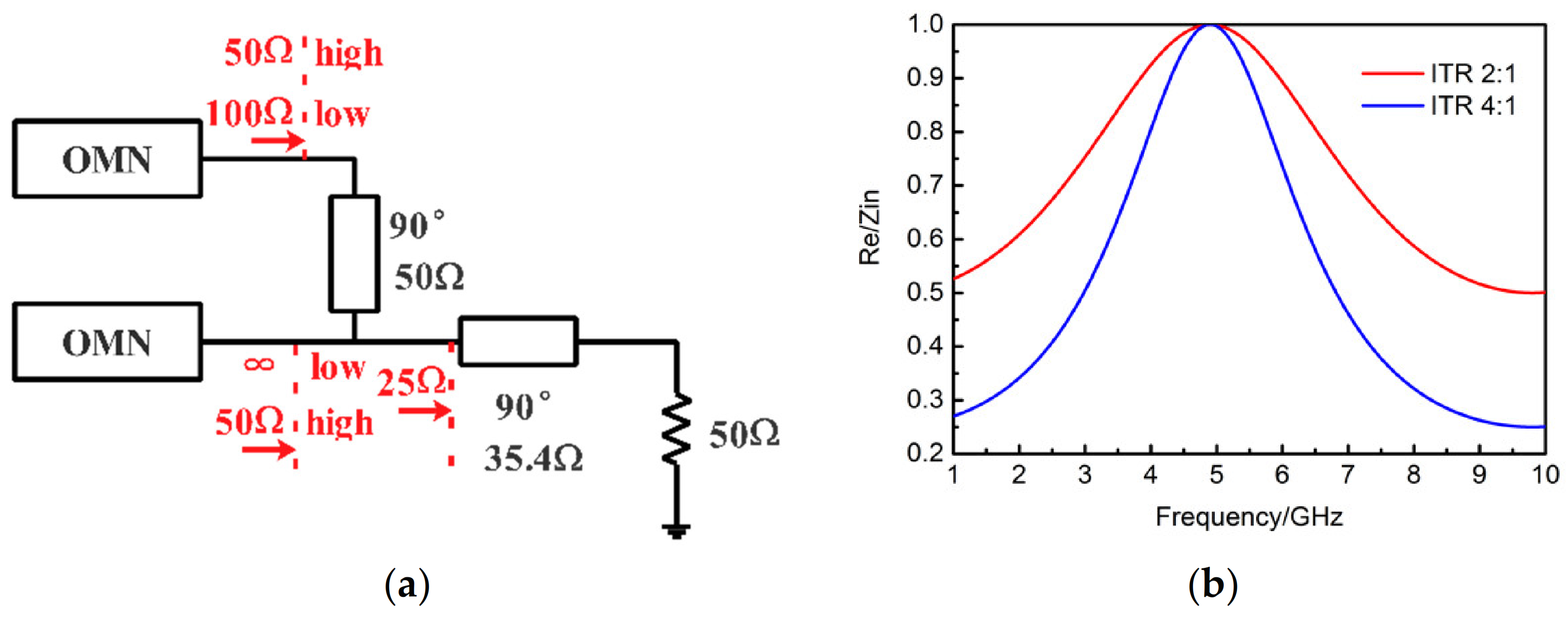
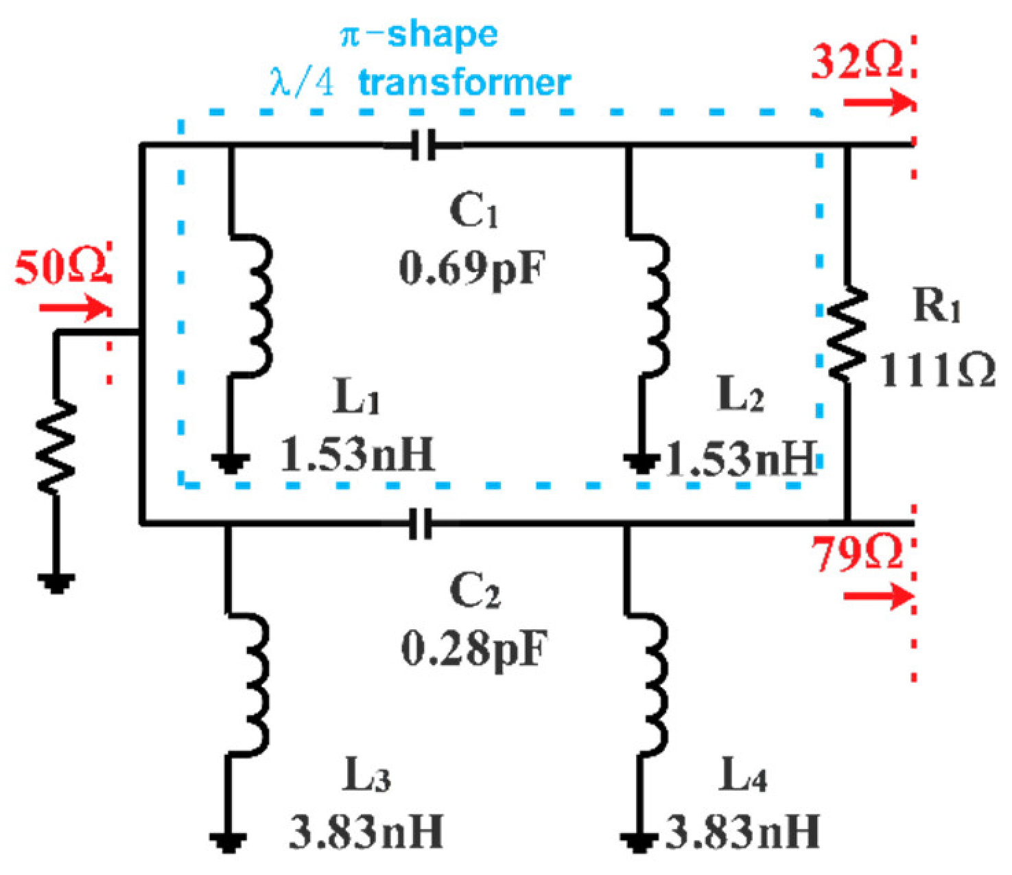
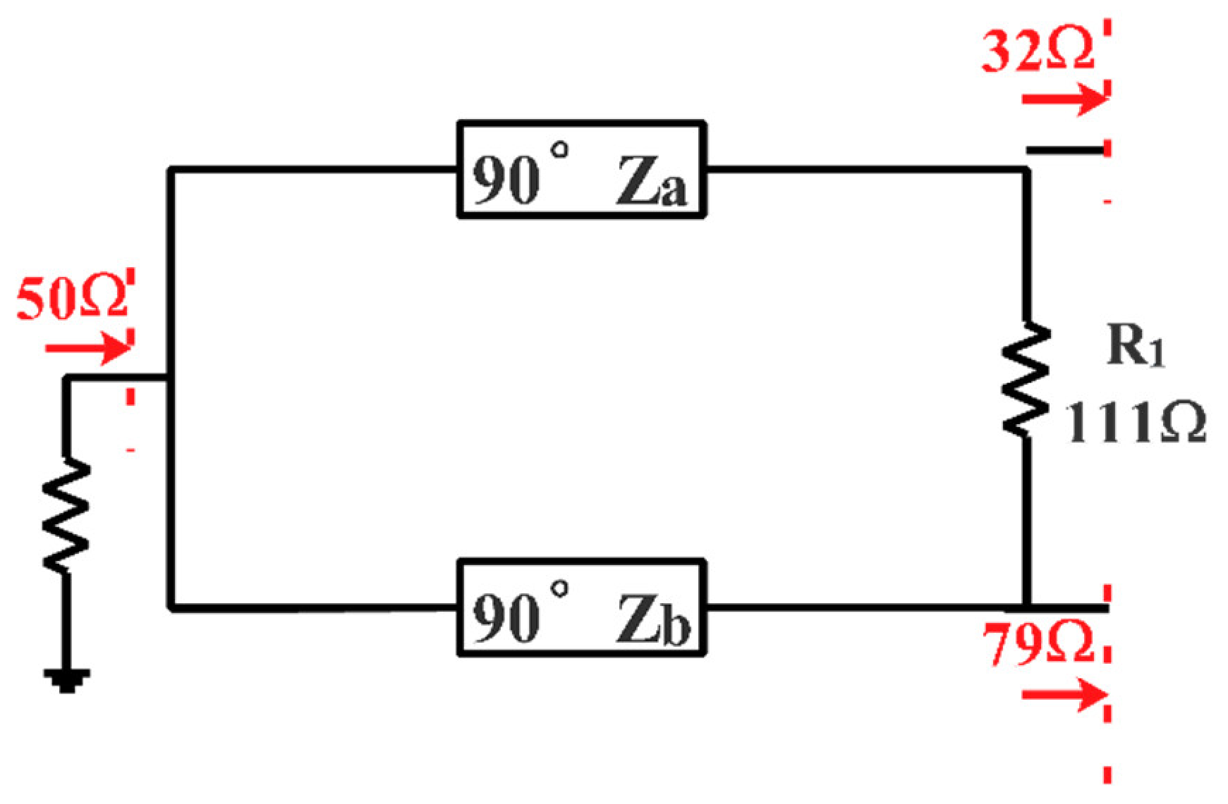
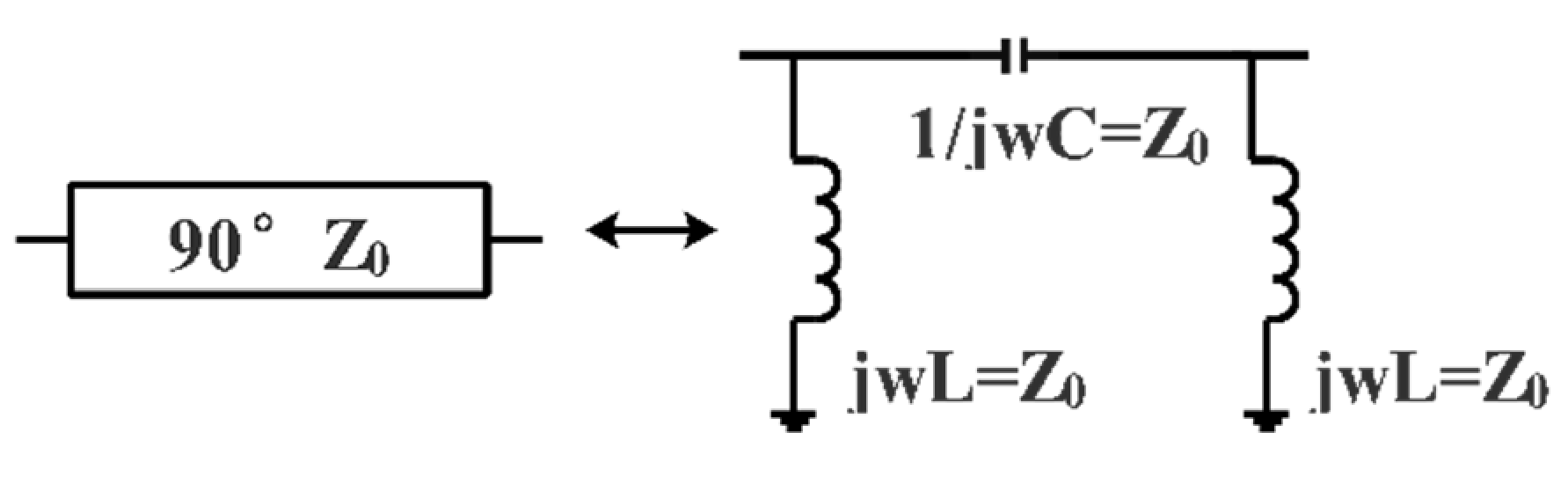
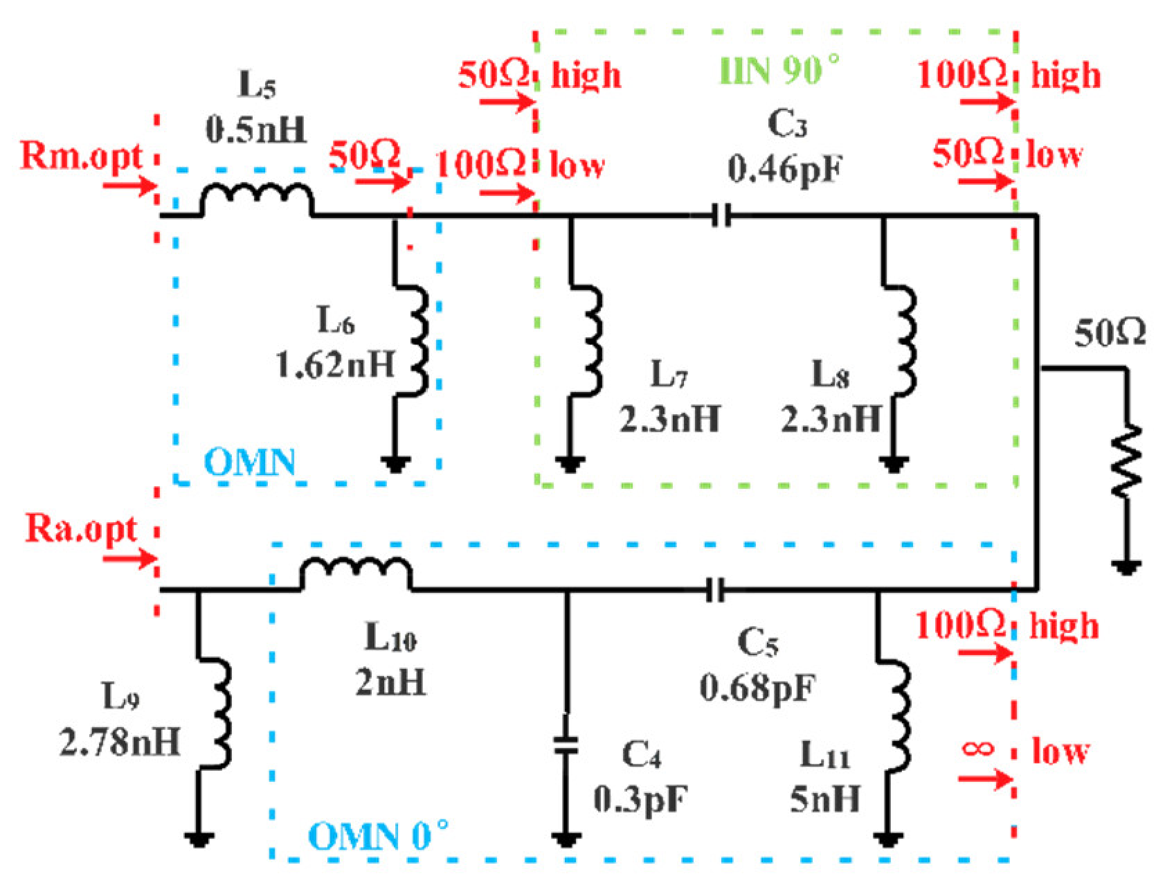
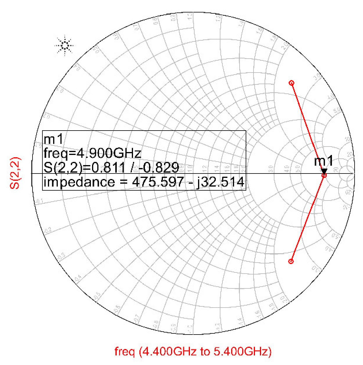
2.3. Design of OMN
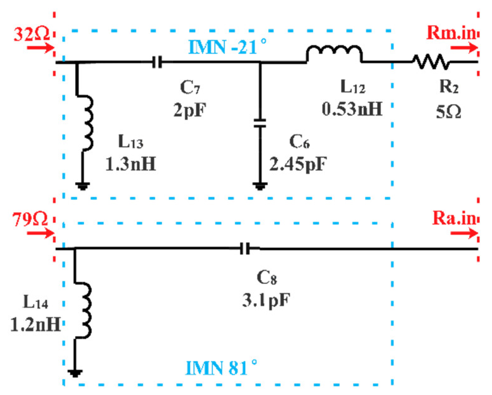
2.4. Design of IMN
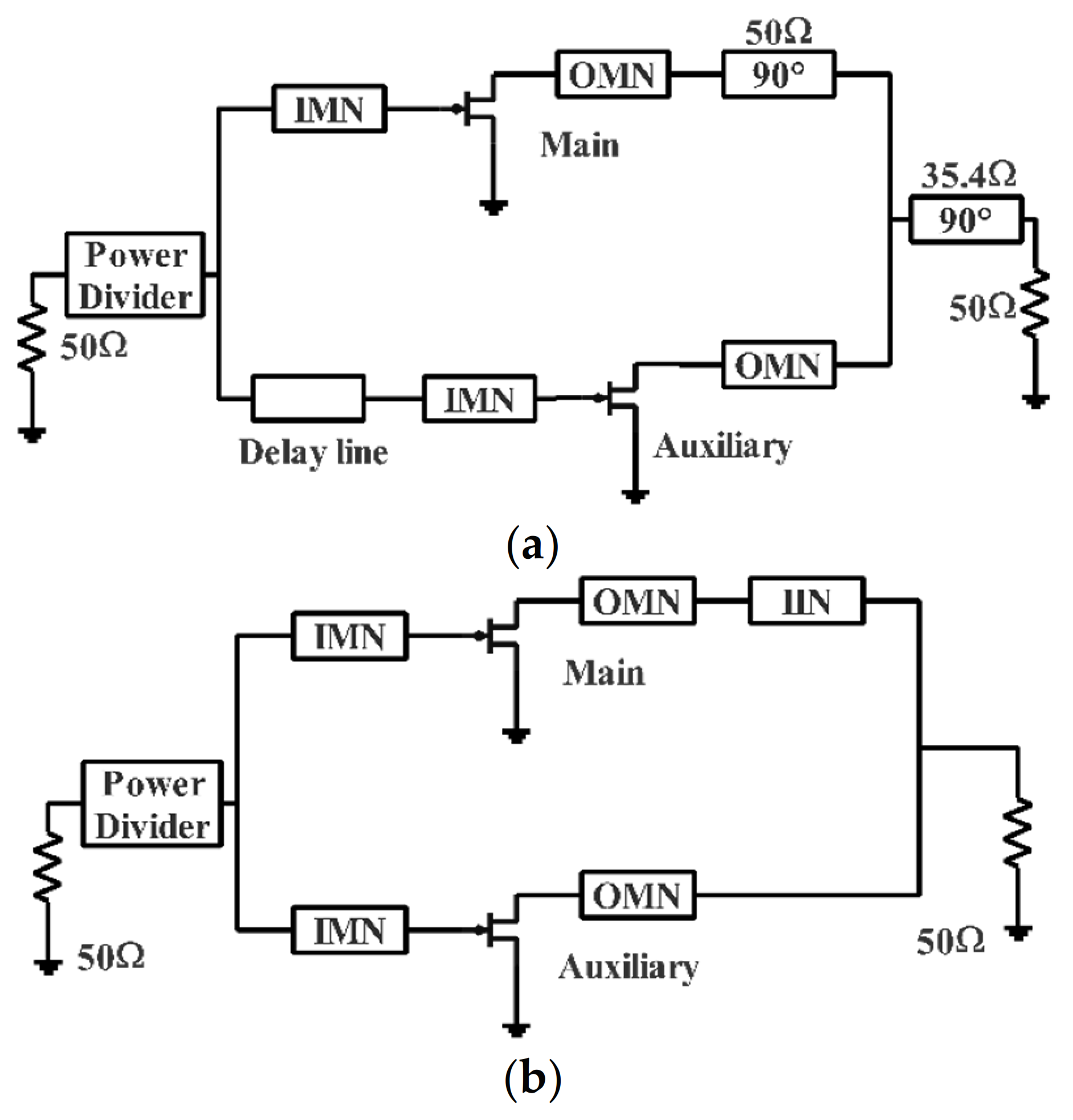
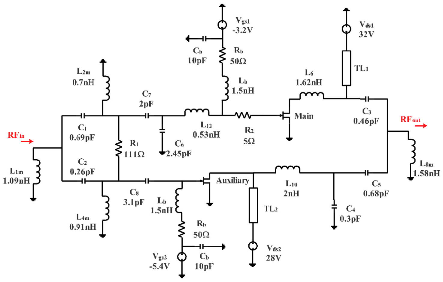
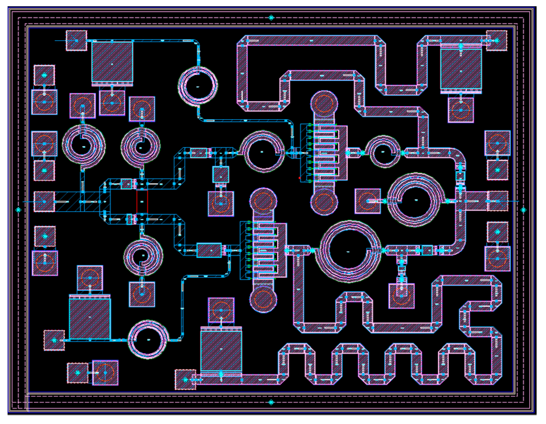
2.5. The Implementation of DPA
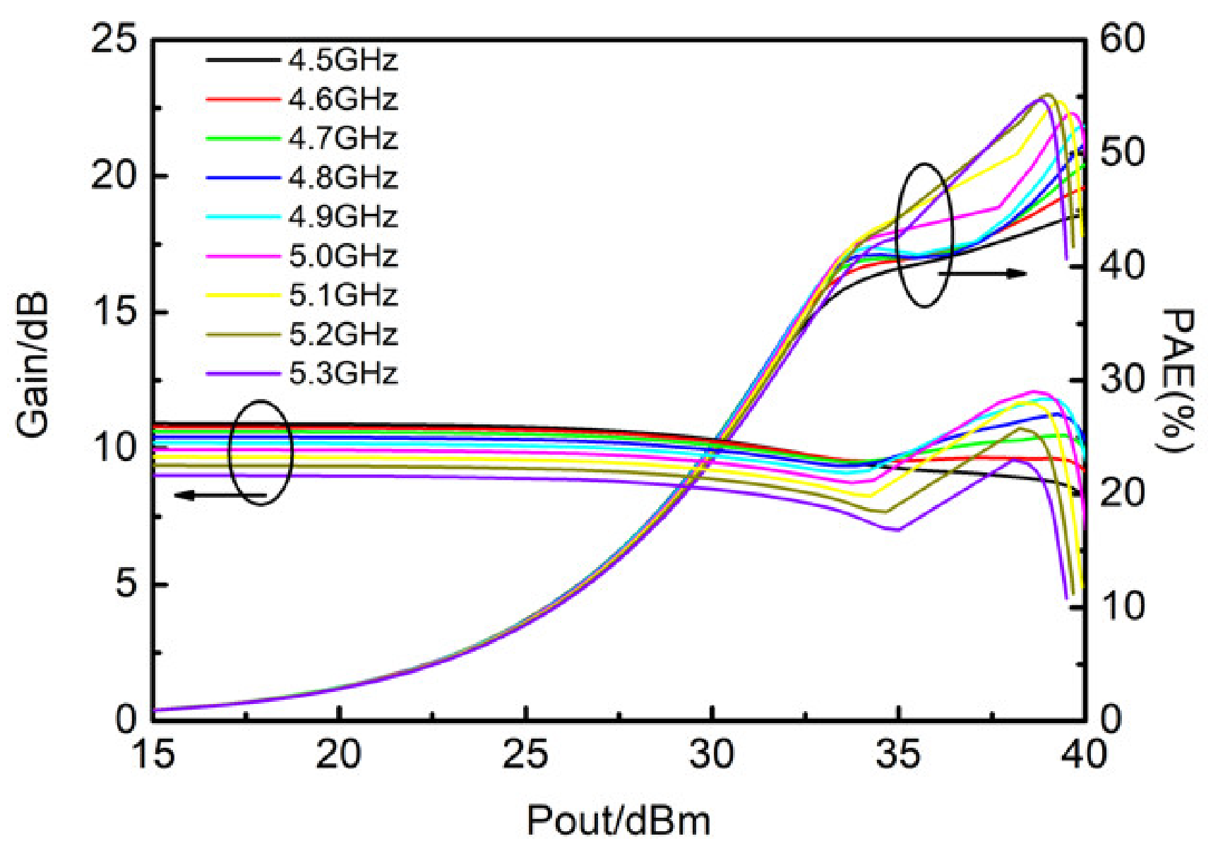
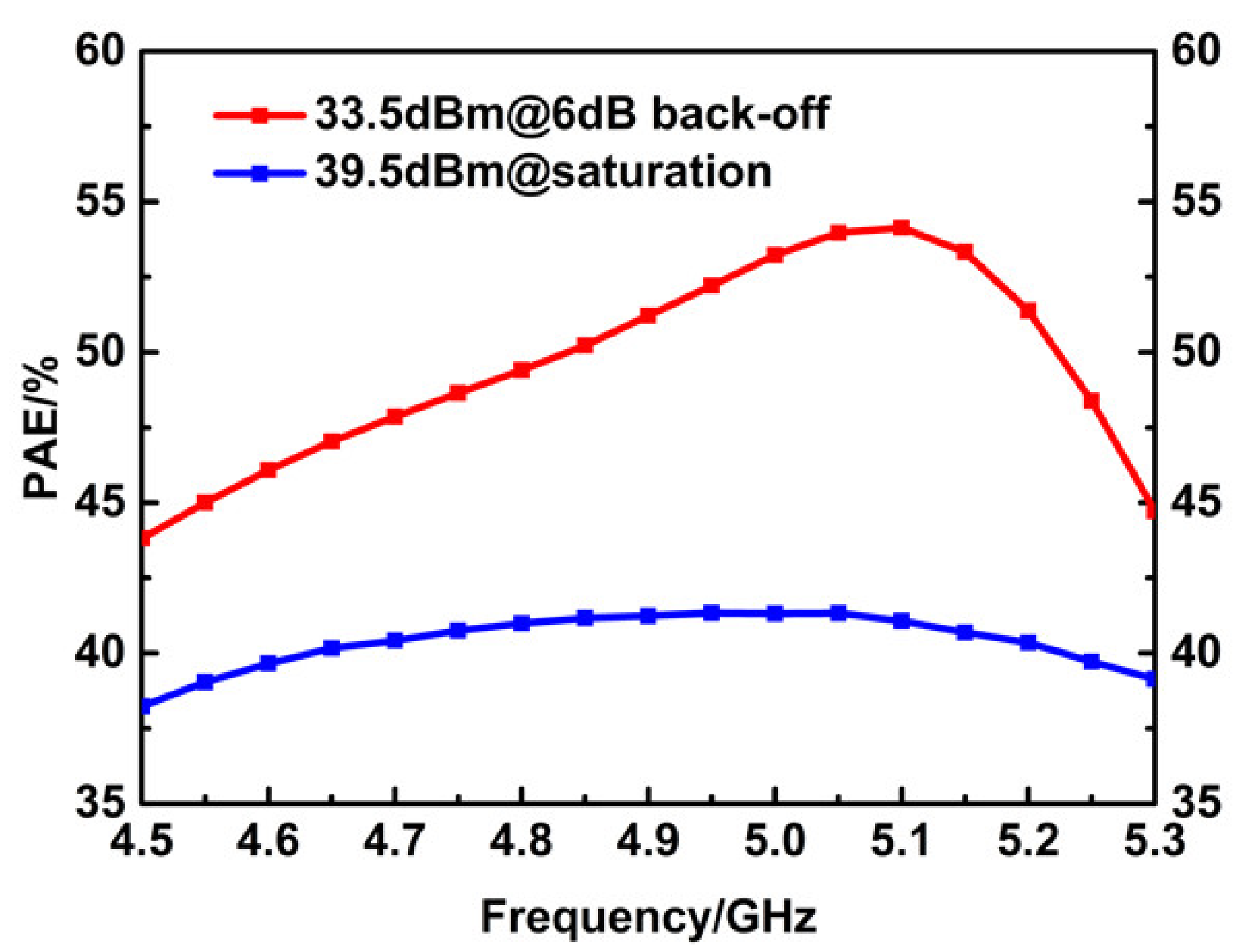
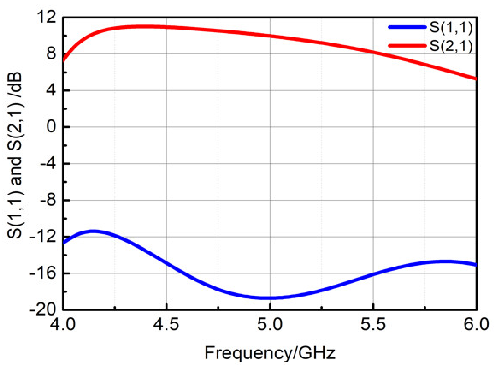
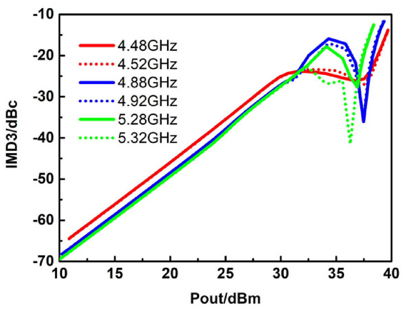
3. Simulation Results
4. Conclusions
Author Contributions
Funding
Conflicts of Interest
References
- Andrews, J.G.; Buzzi, S.; Choi, W.; Hanly, S.V.; Lozano, A.; Soong, A.C.K.; Zhang, J.C. What Will 5G Be? IEEE J. Sel. Areas Commun. 2014, 32, 1065–1082. [Google Scholar] [CrossRef]
- Popovic, Z. Amping Up the PA for 5G: Efficient GaN Power Amplifiers with Dynamic Supplies. IEEE Microw. Mag. 2017, 18, 137–149. [Google Scholar] [CrossRef]
- Sajedin, M.; Elfergani, I.T.E.; Rodriguez, J.; Abd-Alhameed, R.A.; Abdulkhaleq, A.M.; Parchin, N.O.; Al-Yasir, Y.I.A. A Doherty Power Amplifier Based on the Harmonic Generating Mechanism. In Proceedings of the 2020 14th European Conference on Antennas and Propagation (EuCAP), Copenhagen, Denmark, 15–20 March 2020; pp. 1–5. [Google Scholar]
- Doherty, W.H. A New High Efficiency Power Amplifier for Modulated Waves. Proc. Inst. Radio Eng. 1936, 24, 1163–1182. [Google Scholar] [CrossRef]
- Zhou, X.Y.; Chan, W.S.; Pang, J.; Xia, J.; Feng, W. Broadband Doherty-Like Power Amplifier Using Paralleled Right- and Left-Handed Impedance Transformers. IEEE Trans. Microw. Theory Tech. 2020, 68, 4599–4610. [Google Scholar] [CrossRef]
- Zhou, X.Y.; Chan, W.S.; Chen, S.; Feng, W.J. Broadband Highly Efficient Doherty Power Amplifiers. IEEE Circuits Syst. Mag. 2020, 20, 47–64. [Google Scholar] [CrossRef]
- Nikandish, G.; Staszewski, R.B.; Zhu, A.N. Breaking the Bandwidth Limit: A Review of Broadband Doherty Power Amplifier Design for 5G. IEEE Microw. Mag. 2020, 21, 57–75. [Google Scholar] [CrossRef] [Green Version]
- Lv, G.S.; Chen, W.H.; Feng, Z.H. A C-band GaAs Doherty Power Amplifier MMIC with Compact Size and 1-GHz Bandwidth. In Proceedings of the 2018 IEEE Mtt-S International Microwave Workshop Series on 5g Hardware and System Technologies (Imws-5g), Dublin, Ireland, 30–31 August 2018. [Google Scholar]
- Lee, J.; Lee, D.-H.; Hong, S. A Doherty Power Amplifier With a GaN MMIC for Femtocell Base Stations. IEEE Microw. Wirel. Compon. Lett. 2014, 24, 194–196. [Google Scholar] [CrossRef]
- Kim, C.H.; Jee, S.; Jo, G.-D.; Lee, K.; Kim, B. A 2.14-GHz GaN MMIC Doherty Power Amplifier for Small-Cell Base Stations. IEEE Microw. Wirel. Compon. Lett. 2014, 24, 263–265. [Google Scholar] [CrossRef]
- Sajedin, M.; Elfergani, I.T.E.; Rodriguez, J.; Abd-Alhameed, R. Modified Symmetric Three-stage Doherty Power Amplifier for 5G. In Proceedings of the 2019 13th European Conference on Antennas and Propagation (EuCAP), Krakow, Poland, 31 March–5 April 2019. [Google Scholar]
- Maroldt, S.; Ercoli, M. 3.5-GHz Ultra-Compact GaN Class-E Integrated Doherty MMIC PA for 5G massive-MIMO Base Station Applications. Eur. Microw. Integr. 2017, 196–199. [Google Scholar] [CrossRef]
- Lv, G.; Chen, W.; Liu, X.; Ghannouchi, F.M.; Feng, Z. A Fully Integrated C-Band GaN MMIC Doherty Power Amplifier With High Efficiency and Compact Size for 5G Application. IEEE Access 2019, 7, 71665–71674. [Google Scholar] [CrossRef]
- Lv, G.; Chen, W.; Liu, X.; Feng, Z. A Dual-Band GaN MMIC Power Amplifier With Hybrid Operating Modes for 5G Application. IEEE Microw. Wirel. Compon. Lett. 2019, 29, 228–230. [Google Scholar] [CrossRef]
- Li, S.H.; Hsu, S.S.H.; Zhang, J.; Huang, K.C. A Sub-6 GHz Compact GaN MMIC Doherty PA with a 49.5% 6 dB back-off PAE for 5G Communications. In In Proceedings of the IEEE/MTT-S International Microwave Symposium-IMS, Pennsylvania, PA, USA, 10–15 June 2018; pp. 805–807. [Google Scholar] [CrossRef]
- Bhardwaj, S.; Kitchen, J. Broadband Parallel Doherty Power Amplifier in GaN for 5G Applications. In Proceedings of the IEEE Topical Conference on RF/Microwave Power Amplifiers for Radio and Wireless Applications (PAWR), Orlando, FL, USA, 20–23 January 2019; pp. 228–230. [Google Scholar] [CrossRef]
- Liu, R.J.; Zhu, X.W.; Jiang, X.; Xia, D. A 4.9-GHz GaN MMIC Doherty Power Amplifier for 5G Application. In In Proceedings of the 2019 IEEE International Symposium on Radio-Frequency Integration Technology (Rfit2019), Nanjing, China, 28–30 August 2019. [Google Scholar]
- Youngoo, Y.; Jeonghyeon, C.; Bumjae, S.; Bumman, K. A fully matched N-way doherty amplifier with optimized linearity. IEEE Trans. Microw. Theory Tech. 2003, 51, 986–993. [Google Scholar] [CrossRef]
- Liu, M.; Fang, X.; Huang, H.; Boumaiza, S. Dual-band 3-way Doherty Power Amplifier with Extended Back-off Power and Bandwidth. IEEE Trans. Circuits Syst. II Express Briefs 2019. [Google Scholar] [CrossRef]
- Kang, H.; Lee, H.; Oh, H.; Lee, W.; Park, C.S.; Hwang, K.C.; Lee, K.Y.; Yang, Y. Symmetric Three-Way Doherty Power Amplifier for High Efficiency and Linearity. IEEE Trans. Circuits Syst. II Express Briefs 2017, 64, 862–866. [Google Scholar] [CrossRef]
- Wong, J.; Watanabe, N.; Grebennikov, A. High-Power High-Efficiency Broadband GaN HEMT Doherty Amplifiers for Base Station Applications. In Proceedings of the 2018 IEEE Topical Conference on RF/Microwave Power Amplifiers for Radio and Wireless Applications (PAWR), Anaheim, CA, USA, 14–17 Jane 2018; pp. 16–19. [Google Scholar]
- Liu, G.; Cheng, Z.; Zhang, M.; Chen, S.; Gao, S. Bandwidth enhancement of three-device Doherty power amplifier based on symmetric devices. IEICE Electron Express 2018, 15, 20171222. [Google Scholar] [CrossRef] [Green Version]
- Huang, C.; He, S.; You, F. Design of Broadband Modified Class-J Doherty Power Amplifier With Specific Second Harmonic Terminations. IEEE Access 2018, 6, 2531–2540. [Google Scholar] [CrossRef]
- Fang, X.H.; Cheng, K.-K.M. Extension of High-Efficiency Range of Doherty Amplifier by Using Complex Combining Load. IEEE Trans. Microw. Theory Tech. 2014, 62, 2038–2047. [Google Scholar] [CrossRef]
- Abdulkhaleq, A.M.; Yahya, M.A.; McEwan, N.; Rayit, A.; Abd-Alhameed, R.A.; Ojaroudi Parchin, N.; Al-Yasir, Y.I.A.; Noras, J. Recent Developments of Dual-Band Doherty Power Amplifiers for Upcoming Mobile Communications Systems. Electronics 2019, 8. [Google Scholar] [CrossRef] [Green Version]
- Nikandish, G.; Staszewski, R.B.; Zhu, A. Bandwidth Enhancement of GaN MMIC Doherty Power Amplifiers Using Broadband Transformer-Based Load Modulation Network. IEEE Access 2019, 7, 119844–119855. [Google Scholar] [CrossRef]
- Quaglia, R.; Pirola, M.; Ramella, C. Offset Lines in Doherty Power Amplifiers: Analytical Demonstration and Design. IEEE Microw. Wirel. Compon. Lett. 2013, 23, 93–95. [Google Scholar] [CrossRef]
- Seunghoon, J.; Juyeon, L.; Junghwan, S.; Seokhyeon, K.; Cheol Ho, K.; Junghwan, M.; Bumman, K. Asymmetric Broadband Doherty Power Amplifier Using GaN MMIC for Femto-Cell Base-Station. IEEE Trans. Microw. Theory Tech. 2015, 63, 2802–2810. [Google Scholar] [CrossRef]
- Kang, D.; Kim, D.; Cho, Y.; Park, B.; Kim, J.; Kim, B. Design of Bandwidth-Enhanced Doherty Power Amplifiers for Handset Applications. IEEE Trans. Microw. Theory Tech. 2011, 59, 3474–3483. [Google Scholar] [CrossRef]
- Jangheon, K.; Jeonghyeon, C.; Ildu, K.; Bumman, K. Optimum operation of asymmetrical-cells-based linear Doherty power Amplifiers-uneven power drive and power matching. IEEE Trans. Microw. Theory Tech. 2005, 53, 1802–1809. [Google Scholar] [CrossRef]


| Parameter | Reference [15] | Reference [17] | Reference [26] | This Work |
|---|---|---|---|---|
| Fre (GHz) | 5.9 | 4.8–5.0 | 4.5–6.0 | 4.5–5.3 |
| Gain (dB) | 14.4 | 9 | 11.6 | 11 |
| Psat (dBm) | 38.7 | 40.3 | 36 | 39.5 |
| PAE (sat) | 47.3% | 60–63%(DE) | 25.7% | 44–54% |
| PAE (back-off) | 49.5%@6 dB | 51–53%(DE)@6 dB | 22.5–27.6%@8 dB | 38–41.3%@6 dB |
| Size (mm2) | 2.49 × 1.56 | 2.5 × 2.3 | 3.0 × 2.8 | 2.37 × 1.86 |
Publisher’s Note: MDPI stays neutral with regard to jurisdictional claims in published maps and institutional affiliations. |
© 2021 by the authors. Licensee MDPI, Basel, Switzerland. This article is an open access article distributed under the terms and conditions of the Creative Commons Attribution (CC BY) license (http://creativecommons.org/licenses/by/4.0/).
Share and Cite
Cheng, P.; Wang, Q.; Li, W.; Jia, Y.; Liu, Z.; Feng, C.; Jiang, L.; Xiao, H.; Wang, X. A Broadband Asymmetrical GaN MMIC Doherty Power Amplifier with Compact Size for 5G Communications. Electronics 2021, 10, 311. https://doi.org/10.3390/electronics10030311
Cheng P, Wang Q, Li W, Jia Y, Liu Z, Feng C, Jiang L, Xiao H, Wang X. A Broadband Asymmetrical GaN MMIC Doherty Power Amplifier with Compact Size for 5G Communications. Electronics. 2021; 10(3):311. https://doi.org/10.3390/electronics10030311
Chicago/Turabian StyleCheng, Peisen, Quan Wang, Wei Li, Yeting Jia, Zhichao Liu, Chun Feng, Lijuan Jiang, Hongling Xiao, and Xiaoliang Wang. 2021. "A Broadband Asymmetrical GaN MMIC Doherty Power Amplifier with Compact Size for 5G Communications" Electronics 10, no. 3: 311. https://doi.org/10.3390/electronics10030311
APA StyleCheng, P., Wang, Q., Li, W., Jia, Y., Liu, Z., Feng, C., Jiang, L., Xiao, H., & Wang, X. (2021). A Broadband Asymmetrical GaN MMIC Doherty Power Amplifier with Compact Size for 5G Communications. Electronics, 10(3), 311. https://doi.org/10.3390/electronics10030311