Article

Battery Charger Based on a Resonant Converter for High-Power LiFePO4 Batteries

by
Christian Brañas
1,*,
Juan C. Viera
2,
Francisco J. Azcondo
1,
Rosario Casanueva
1,
Manuela Gonzalez
2 and
Francisco J. Díaz
1
1
Electronics Technology, Systems and Automation Engineering Department, University of Cantabria, 39005 Santander, Spain
2
Department of Electrical Engineering, University of Oviedo, Campus de Gijón, Módulo 3, 33204 Gijón, Spain
*
Author to whom correspondence should be addressed.
Electronics 2021, 10(3), 266; https://doi.org/10.3390/electronics10030266
Submission received: 21 December 2020 / Revised: 20 January 2021 / Accepted: 21 January 2021 / Published: 23 January 2021

Abstract

:
A new battery charger, based on a multiphase resonant converter, for a high-capacity 48 V LiFePO4 lithium-ion battery is presented. LiFePO4 batteries are among the most widely used today and offer high energy efficiency, high safety performance, very good temperature behavior, and a long cycle life. An accurate control of the charging current is necessary to preserve the battery health. The design of the charger is presented in a tight correlation with a battery model based on experimental data obtained at the laboratory. With the aim of reducing conduction losses, the general analysis of the inverter stage obtained from the parallel connection of N class D LCpCs resonant inverters is carried out. The study provides criteria for proper selection of the transistors and diodes as well as the value of the DC-link voltage. The effect of the leakage inductance of the transformer on the resonant circuit is also evaluated, and a design solution to cancel it is proposed. The output stage is based on a multi-winding current-doubler rectifier. The converter is designed to operate in open-loop operation as an input voltage-dependent current source, but in closed-loop operation, it behaves as a voltage source with an inherent maximum output current limitation, which provides high reliability throughout the whole charging process. The curve of efficiency of the proposed charger exhibits a wide flat zone that includes light load conditions.

1. Introduction

Lithium iron phosphate (LiFePO4) batteries have a great electrochemical performance and a good thermal stability, which makes them safer and more robust. This lithium-based technology exhibits a very low internal resistance offering a high current rating. Their cycle life is significantly longer compared to other technologies [1,2]. The applications of LiFePO4 batteries are, among others, for storage systems in renewable energy facilities, powering electric vehicles and uninterruptible power supplies (UPS) in data centers, telecommunications, and hospitals. A battery model is an important tool for designing the charger allowing the study of the dynamic response of the battery-charger system along the whole charging process, wherein the converter load, i.e., the equivalent resistance of the battery, varies from almost short-circuit to open-circuit values. Most of the battery models are aimed to improve the battery management system (BMS) performance, providing information about important parameters of the battery such as the state of charge (SOC) [3]. The estimation of the battery SOC and power capacity is usually solved by applying three methods, i.e., the look-up table method, the model-based method, and the artificial intelligence method [4,5,6,7]. In addition to that, the BMS is responsible for ensuring the battery operation within safety margins of temperature and sets the overvoltage and under voltage protection limits. In this work, the battery modeling is presented in a tight correlation with the battery charger design.
The technology of resonant converters is chosen to implement the proposed battery charger. The advantages of the resonant conversion of energy, such as high frequency of operation, sinusoidal waveforms, and low switching losses are well known [8]. Among all possible configurations of resonant converters, the series resonant converter and the LLC converter have been widely used [9,10,11,12]. Usually, the converter is designed to operate as a voltage source with some kind of control to limit the charging current. In this work, the converter is designed as a voltage-dependent current source. In this approach, the circuit presents an inherent maximum current limitation, which is a safer operation mode. The LiFePO4 technology reaches current rates as high as hundreds of amps. In circuit design for high-current applications, conduction losses are a major design limitation [13,14]. In high-current resonant converters, increasing the dc-link voltage, Vdc, and using a step-down transformer (n > 1) reduces the amplitude of the resonant currents in the inverter stage, minimizing the conduction loss in transistors and resonant inductors. New Wide Band Gap (WBG) devices enable the operation at an 800 V to 1700 V dc-link voltages range [15]. WBG devices achieve high performance at high current levels with important simplifications in the power circuit. However, the cost of WBG devices limits their use for certain applications.
In this work, a generalized design method aimed at minimizing the conduction loss is presented for multiphase resonant converters [16]. The number of parallel branches and therefore phases, N, in the inverter stage is calculated according to the maximum output power and the expected efficiency. This alternative offers another degree of freedom for achieving efficiencies higher than 90% even at relatively low values of Vdc and using low-cost transistors. Moreover, the multi-phase structure makes it possible to regulate the charging current at constant switching frequency by shifting the phase of the output voltages of each class D section of the inverter.
This paper is organized as follows: After the introduction, Section 2 describes the charging profile of the target LiFePO4 battery, which is oriented to obtain a fast charge without reducing its lifetime. The battery model is presented in Section 3. The analysis of the proposed charger and main design equations are developed in Section 4. The efficiency of the charger is studied in Section 5. A detailed step-by-step design sequence of the proposed charger is explained in Section 6. In Section 7 and Section 8, the results obtained for the modeling of the battery and experimental waveforms to verify the performance of the prototype are presented, ending with a discussion about Si vs. SiC solutions and concluding remarks.

2. Charging Method

The main characteristics of the commercial 48NPFC50 LiFePO4 battery (Narada Power Source Co., Ltd., Hangzhou, China) [17] used in this work are 48 V nominal voltage and 50 Ah nominal capacity (Cn) i.e., 2.4 kWh of power capacity. The battery consists of fifteen (Ns = 15) stacked cells in series and incorporates a BMS that guarantees the right balance-of-charge of all cells. Thus, the voltage across each cell is assumed identical to any other. The battery charger is designed to meet all operational limits settled by the BMS.
The charging protocol recommended for LiFePO4 batteries is the well-known [18] constant current (CC)–constant voltage (CV) method (i.e., CC–CV). During the CC stage, the battery is charged at the maximum current rate, which depends on the battery capacity and technology. Once the battery voltage reaches its maximum charging voltage specified in the battery data sheet, the CV stage begins. At this point, the power drawn from the charger is the maximum, which happens at 90% of the SOC approximately. During the CV stage, the charging current diminishes. Three experimental charging profiles are carried on at the battery laboratory facility shown in Figure 1. They are evaluated at room temperature (25 °C) using the battery test equipment PEC SBT-10050 (PEC, Leuven, Belgium) and taking into account that the battery is fully discharged as the initial condition.
Those profiles correspond to the battery charge at current rates equal to Cn/5, Cn/2, and Cn during the CC stage. The results are shown in Figure 2.
The temperature is observed by the BMS during the whole charging process, and it implements the corresponding protection (maximum value 55 °C for charging) to prevent the battery aging. Electro-thermal models for studying the temperature of a lithium-ion cell as a function of the charging/discharging current have been reported in [19,20]. The user manual recommends a conservative value, Cn/5, for the charging current rate; however, LiFePO4 technology tolerates fast-charging protocols [21,22,23,24]. In this work, in order to shorten the charging time, a maximum charging current rate of 20 A (approximately Cn/2) is chosen the charger design. According to the experimental characterization of the battery, charging at Cn/2 keeps the temperature of the battery well below 55 °C.

3. Battery Model

Although the LiFePO4 cell is a complex physical system with several variables involved, a good trade-off among simplicity, accuracy, and insight information is obtained with the electrical parameters-based models [25], as shown in Figure 3. The single cell model is generalized by affecting all parameters by the total number of cells, Ns, under the assumption that all cells are identical, as shown in Figure 3.
The state of charge (SOC) [26] of the battery is defined as the ratio of the battery charge, Q, to the nominal capacity, Cn.
S O C = Q C n · 100 %
The model calculates the SOC [26], integrating the battery current-dependent current source, ibat, which charges/discharges the capacitor Cn. The SOC is equal to the voltage across the capacitor Cn, vCn varying from zero to one corresponding to exhausted to fully charged battery, respectively.
S O C ( t ) = S O C ( t o ) + 1 C n t o t i b a t t d t
The voltage-controlled voltage source, Nsvqoc(SOC), dependent on the voltage vCn, represents the quasi-open-circuit battery voltage, where vqoc, is the quasi-open-circuit voltage across one single cell. The experimental measurement of vqoc as a function of the SOC is a time-consuming task because it should be obtained while keeping the cell in electrochemical equilibrium [27], charging and discharging the cell at a very low current rate. From the experimental study of one single cell, the vqoc as a function of the SOC was obtained by charging and discharging the cell at Cn/50. This test required 100 h. The result is shown in Figure 4.
As it is observed in Figure 4, the quasi-open-circuit cell voltage, vqoc, incorporates the effect of the voltage hysteresis caused by the battery structure [27]. The maximum hysteresis is about ≈ 40 mV within the 30% SOC region, and the average is ≈ 20 mV within the 40% to 80% SOC region. The experimental test results show a cell capacity Cn = 50 Ah, which is represented in the model by a capacitance Cn = 180,000 F.
The electrolyte and electrode resistance are modeled by RΩ. In addition to that, the model also includes two time constants, which are modeled by networks RtCt and RdCd. The time constant RtCt is associated to chemical reactions and charge transportation phenomenon in the electrodes. This time constant is within the range from milliseconds to a few seconds. In contrast, the time constant RdCd governs the mass diffusion in the electrolyte and electrodes and is within the tens of seconds range [27]. From the point of view of the battery charger design, the electrical parameters of the battery at the end of the CC stage are of interest. At this point, the power supplied by the charger is the maximum. For a given SOC, the battery model can be simplified to a resistance, rBat, in series with a voltage source equal to the quasi-open-circuit voltage NsVqoc. Assuming the battery is in steady state, rbat is obtained from the model shown in Figure 3 as
r B a t = N s · R Ω + R t + R d .
The specific values Rt and Rd for a given SOC should be obtained from the dynamic study of the battery, once the time constants associated with transport and diffusion phenomena were obtained. Finally, the battery voltage is obtained as:
V B a t = N s V q o c + I B a t r B a t .

4. Multiphase LCpCs Resonant Converter

The proposed battery charger is a multiphase resonant converter. The general form of the circuit is shown in Figure 5, where the battery is modeled in steady state by its internal impedance, rBat, in series with the quasi-open-circuit battery voltage NsVqoc.
The AC side is a multiphase resonant inverter, which consists of N paralleled LCpCs class D sections [16,28]. Among the possible configurations of the resonant network, the configuration LCpCs of the LCC family is chosen to achieve a current source behavior while preserving the zero voltage switching (ZVS) mode of transistors [8,29]. Unlike the LLC converter, the proposed LCpCs does not require a gapped-core transformer [30], so the magnetizing inductance, LM, is high enough to neglect its impact in the later analysis.
The DC side consists of an M-winding current multiplier, which is derived from the parallel connection of an M current-doubler rectifier [31,32]. The low output voltage of this application recommends the use of Schottky diodes without any control circuit in the secondary side, which is a simplification in comparison to solutions based on synchronous rectification (SR).

4.1. Resonant Inverter Stage

The converter is analyzed considering the general case, where each midpoint voltage vi of all class D sections has associated a phase-angle Ψ0, Ψ1, …, Ψi−1. To illustrate this assumption, the midpoint voltages, vi, are shown in Figure 6.
Using the fundamental approximation, the input voltages, vi, are represented with the exponential form given in (5),
V i = 2 V d c π · e j Ψ i 1 ,
where i ∈ [1, 2, …, N] is the phase number. In steady state and using the low ripple approximation, the M-winding output rectifier is reduced to an equivalent impedance Rac [8,29]. The resonant inverter stage is analyzed using the simplified circuit model shown in Figure 7.
The parallel parameters of the resonant inverter are defined in Table 1.

4.1.1. AC Side Output Current

During the CC stage of the charging process, the converter provides an inherent current limitation, protecting the battery and extending its life. The current source behavior of the resonant converter is achieved by fixing the switching frequency at ω = ωp, where ωp is the parallel resonant frequency, as given in Table 1. Once the switching frequency is fixed at ω = ωp, the output current, seen from the primary side of the transformer, i.e., through Cs, Iac, is calculated by (6).
I ac = 2 V d c π Z p m = 1 N sin Ψ m 1 + j m = 1 N cos Ψ m 1
From (6), the current source behavior is verified, given that Iac has no dependence on the load.

4.1.2. Switching Mode

The switching losses are minimized by ensuring the zero voltage switch (ZVS) on the primary side of the converter [8,29]. The ZVS mode requires sufficient phase-delay of the resonant current with respect to the input voltage. A high value of Qp reduces the reactive energy in the resonant converter, which is beneficial from the point of view of reducing the conduction loss. However, some reactive energy must be accepted for ensuring the ZVS mode of all transistors. The complex form, Ii, of each resonant current is given in (7) as a function of the angles Ψ0, Ψ1, …, ΨN−1.
I i = 2 V d c π Z p × Q p N m = 1 N cos Ψ m 1 C p N C s L k L m = 1 N sin Ψ m 1 sin Ψ i 1 j Q p N m = 1 N sin Ψ m 1 + C p N C s L k L m = 1 N cos Ψ m 1 + cos Ψ i 1
In order to determine the power factor angle, ϕi, of each transistor’s leg, the input impedance Zi = Vi/Ii, of each phase is calculated. The power factor angle, ϕi is obtained using ϕi = angle(Zi) as a function of the control angles, Ψ0, Ψ1, …, ΨN−1, the number of phases, N, and the quality factor, Qp. Upon substitution of Ψ0 = Ψ1 = …ΨN−1 = 0° in (5) and (7), ϕi at the maximum output current is obtained:
ϕ i = arctan 1 + C p C s N L k L Q p .
From (8), it can be observed that the effect of leakage inductance referred to the primary side of the transformer, Lk, is more significant for high-power as well as for high-frequency designs, where the value of inductance of the resonant circuit, L, is usually low, and a high value of leakage inductance could produce the loss of the ZVS mode. However, the series disposition of Lk and Cs enables the cancelation of the Lk effect on the AC side by calculating Cs to achieve, at the switching frequency, the series resonance with Lk. According to this proposal, Cs is obtained from (9).
C s = L N L k C p
With the cancellation of the Lk effect, the value of the power factor angle, ϕi, depends essentially on the value of the quality factor Qp, which is set during the design process of the converter. The minimum value of power factor angle for achieving ZVS, ϕzvs, depends on the dead time, td, of the transistors’ driver and the switching frequency ωp [33].
φ z v s = t d ω p 2 π · 360 °
As design criteria, a value of power factor angle ϕi = 2ϕzvs is assumed at nominal conditions for achieving a reliable operation of the converter. This is the most restrictive design condition for operating in ZVS mode for the whole range of variation of the control angle Ψ. From (8) to (10), the value of the quality factor at nominal conditions, QpN, is obtained:
Q p N = 1 tan 2 φ z v s

4.1.3. Variation of the Quality Factor and Transformer Turns Ratio

During the charging process, the equivalent impedance of the battery, RBat, changes depending on VBat and IBat, whose relationship is given by the charging profile of the battery, as shown in Figure 1. At the end of the CC stage, VBat = VBat(Max) and the power supplied to the battery reaches the maximum, PBat = VBat(Max)IBat(Max). The specifications of the point of maximum output power are used for defining the nominal value of the quality factor, QpN. Thus, during the CC stage of the charging profile, the converter works with a quality factor lower than the nominal one, which strengthens the inductive behavior of the resonant tank, assuring the ZVS mode.
During the CV stage, the reduction of the charging current leads to a significant increment in the equivalent resistance RBat and consequently, the reflected impedance on the AC side, Rac, and the quality factor Qp also increase. Assuming that VBat(Max) is constant and working with (6), the quality factor as a function of Ψ is obtained in (12),
Q p = n π 2 V B a t ( M a x ) 2 V d c N m = 1 N sin Ψ m 1 2 + m = 1 N cos Ψ m 1 2
The increment of Qp, as a consequence of the reduction of the charging current during the CV stage could put at risk the ZVS mode of the transistors of the converter. However, it is beneficial from the point of view of achieving waveforms with low distortion and increases the converter efficiency. The nominal value of quality factor is obtained by evaluating (12) for Ψ0 = Ψ1 = ΨN−1 = 0°.
Q p N = n π 2 V B a t ( M a x ) 2 V d c
From (13) and (11), the transformer’s turns ratio (n:1) can be obtained:
n = 2 V d c π 2 V B a t ( M a x ) tan 2 φ z v s .

4.2. Output Current Multiplier

In order to analyze the output current multiplier stage, first, a single-winding current-doubler rectifier with an ideal transformer, as seen in Figure 8, is considered. The quasi-sinusoidal voltage vac at parallel capacitor Cp drives the current multiplier stage. The diodes D1 and D2 turn on alternatively according the positive or negative cycle of vac, respectively.
The diodes conduction time, t1, is obtained from the volts–seconds balance across the inductors. The areas are calculated according to the approximation shown in Figure 8 right.
t 1 = n π 1 + n π T
The average current through each inductor, Lo1,2, is equal to one-half of the charging current IBat. The amplitude of the current ripple in each inductor is determined by
Δ i L = n π 2 V B a t ( M a x ) 1 + n π ω p L o .
The total ripple current through the filter capacitor Co is calculated considering M parallel rectifiers and taking into account the ripple cancellation effect due to the 180° phase displacement between the current through each inductor [31,32] in the current-doubler structure; thus,
Δ i C = n π 2 M V B a t ( M a x ) 2 1 + n π ω p L o
The output voltage ripple is
Δ v B a t = n π 3 M V B a t ( M a x ) 16 1 + n π ω p 2 L o C o
From (18), the ripple of the charging current is a function of the switching frequency, output filter components, and battery parameters.
Δ i B a t = n π 3 M V B a t ( M a x ) 16 1 + n π r B a t ω p 2 L o C o
The limitation of the output current ripple, ΔiBat, is mandatory in order to avoid the battery degradation [12].

Reflected Impedance on the Primary Side of the Transformer

Since the output filter removes the high-frequency ripple, the low ripple approximation [29] is used to study the proposed rectifier in steady state. Considering the total current in the primary side and using the first harmonic of the square waveform, the relationship between the AC and DC currents is given in (20).
I ^ a c = 2 I B a t n π
where Îac is the amplitude of the transformer’s primary current. From (20) and (6), the charging current is obtained as a function of the angles Ψ0, Ψ1, …, ΨN−1,
I B a t = n V d c Z p m = 1 N sin Ψ m 1 2 + m = 1 N cos Ψ m 1 2
The normalized amplitude of the charging current, IBat, is depicted in Figure 9 as a function of the control angle, Ψ, and considering the modulation pattern where all phases are evenly shifted.
Working with (21), the maximum charging current is achieved at Ψ0 = Ψ1 = ΨN−1 = 0° and is given by
I B a t ( M a x ) = n V d c Z p · N
From (22), it can be observed that the output current capability of the multiphase converter is enhanced by increasing the number, N, of paralleled phases. An accurate acquisition of the modulation angle, covering the whole range over the entire battery charging process, facilitates the computation of ampere-hours in order to calculate the supplied capacity.
The amplitude of the voltage in the primary side of the transformer is obtained from the power balance in the windings. Assuming a lossless transformer,
P a c = P B a t = I ^ a c V ^ a c 2 = I B a t V B a t
and substituting (20) into (23),
V ^ a c = n π V B a t = n π r B a t · I B a t + n π · V B a t .
From (20) and (24), the battery is modeled from the AC side by
V ^ a c = n 2 π 2 2 r B a t · I ^ a c + n π · V B a t .
The reflected impedance of the current multiplier and load, Rac, into the AC side of the converter defines important characteristics of the resonant inverter, such as the switching mode of the transistors, the distortion of the waveforms, and the efficiency [11]. From (25), the rectifier stage is reflected into the AC side as the equivalent resistance Rac in (26),
R a c = π 2 2 n 2 R B a t = π 2 2 n 2 r B a t + V B a t I B a t
Assuming an ideal transformer, where the leakage inductance reflected in the secondary side is Lks = 0, the maximum voltage across the diodes is VB = −nπVBat. However, in practice, Lks is in series with the junction capacitance of the reverse-biased diode, Cj, causing a high-frequency oscillation or ringing. The selection of the Schottky devices takes into account the minimization of this effect.

5. Efficiency of the Multiphase LCpCs Resonant Converter

The overall efficiency of the converter is calculated by
η = ηI·ηR,
where ηI is the efficiency of the resonant inverter stage and ηR is the efficiency of the output current multiplier stage.

5.1. Efficiency of the Inverter Stage

Taking into account the ZVS mode operation of the converter, the switching loss is considered negligible in comparison to the conduction loss. The efficiency of the resonant inverter stage, ηI, considering the conduction loss only [16] is
η I = 1 1 + r R a c · k = 1 N I ^ i 2 I ^ a c 2
where Îi is the amplitude of each resonant current given in (7). The resistance r represents the rdson of the transistors as well as the ESR of the inductors. The highest efficiency, ηI(Max), is achieved with Ψ0 = Ψ1 = … = ΨN−1 = 0°. Upon substitution of Ψ0 = Ψ1 = … = ΨN−1 = 0° in (28) and under the assumption that Cs is calculated according to (9), the maximum efficiency as a function of the ratio r/Rac, the nominal value of the quality factor, QpN, and the number of phases, N, is obtained.
η I ( M a x ) = 1 1 + r N R a c · 1 + Q p N 2
From (28), it is observed that ηI(Max) is improved by increasing Rac. The straightforward way to increase Rac is through the larger transformer turns ratio, n. However, it should be considered that QpN increases with n, according to (12), which could jeopardize the ZVS mode of the converter transistors. Taking into account the tight correlation among, N, QpN, n, and r/Rac, the design process oriented to find a suitable value of these parameters involves iterative cycles. Upon the substitution of (12) and (20) into (29), ηI(Max) is obtained as a function of the converter parameters,
η I ( M a x ) = 1 1 + π 2 r I B a t ( M a x ) V B a t ( M a x ) 2 N V d c 2 + 2 r I B a t ( M a x ) n 2 π 2 N V B a t ( M a x ) 1 1 + 2 r I B a t ( M a x ) n 2 π 2 N V B a t ( M a x )
The maximum efficiency of the resonant inverter stage, ηI(Max), improves, approaching one asymptotically as the number of phases, N, increases.

5.2. Efficiency of the Output Current Multiplier

Limiting the current level through the output rectifier stage is a major design challenge oriented to reduce the conduction loss. The proposed M-windings output current multiplier lowers the amplitude of the current through diodes by a factor M and the average current through filters inductors by a factor 2M. An expression for the rectifier efficiency, ηR, only including the conduction loss, is obtained from the analysis of the current paths shown in Figure 7. Considering a lossless transformer, the total power, PT, in the secondary side of the current multiplier is
P T = P B a t + M V D I B a t M + I B a t 2 r D M 2 + I B a t 2 r L F 4 M 2 ,
where PBat is the output power, PBat = VBat·IBat, VD and rD are the voltage and dynamic resistance of the linear model of the diode, and rLF is the ESR of the filter inductor Lo. The efficiency, ηR, is calculated with ηR = PBat/PT,
η R = 1 1 + V D V B a t + r D M + r L F 2 M I B a t V B a t .
The efficiency of the output current multiplier, ηR, is improved by increasing the number of secondary windings, M. The theoretical limit ηR(Max) of ηR is obtained letting M→∞,
η R ( M a x ) = 1 1 + V D V B a t ( M a x ) .
From (32) and (33), it can be observed that the ratio VD/VBat(Max) should be minimized, which confirms the benefit of using Schottky diodes or sync rectifiers to improve the efficiency of the rectifier stage.

5.3. Optimum N and M of Parallelized Stages

The expressions (30) to (33) are used as a criterion to define the appropriate number of phases, N, of the resonant inverter stage as well as the number of secondary windings, M, of the output current multiplier. The maximum efficiency of the inverter section, ηI(Max), and the efficiency of the current multiplier, ηR, are depicted in Figure 10 as a function of N and M.
From a practical point of view, the asymptotic variation of ηR and ηI(Max), shown in Figure 10, limits the maximum values of M and N. The criterion for choosing the suitable values of M and N is a tradeoff between the increment of the efficiency and the circuit complexity. It is assumed that if the increment of efficiency achieved is barely 1%, a higher number of secondary windings M or phases, N, is not justified.

6. Design of the Multiphase LCpCs Resonant Converter

(1)
The maximum battery voltage is set at VBat(Max) = 53.5 V, which is below the overvoltage protection limit (54.7 V) defined by the BMS. The output current capability of the circuit is set to IBat = 20 A in order to shortening the charging time. The equivalent impedance of the battery is RBat = 2.67 Ω. The peak power that must be supplied by the charger is PBat = 1.07 kW. The converter supply voltage is Vdc = 400 V, which is the output voltage of a previous front-end PFC stage. The switching frequency is set at ωp = 2π(125 kHz).
(2)
The drive signals of the transistors are obtained from an integrated circuit IR2111 with a dead time, td = 650 ns. From (10), the minimum value of the power factor angle for each class D section is ϕzvs = 29.25°. Using the design constrain φi = 2ϕzvs = 58° from (11), the nominal value of the quality factor is obtained, QpN = 0.624. The transformer turns ratio, n, is calculated from (14), approximating to the nearest entire value, n = 1.
(3)
The number of phases, N, is calculated taking into account that transistors are low-cost CoolMOSTM SPA11N60C3 (Infineon, Neubiberg, Germany) with rds(on) = 0.38 Ω. Considering the equivalent series resistant (ESR) of the resonant inductors and tracks of the printed circuit board (PCB), a worst case of r = 1 Ω is assumed. Upon substitution in (30), the pair n = 1 and N = 4 yields ηI(Max) = 0.98. This value of efficiency means 21 W power loss in the resonant inverter stage at full load conditions.
(4)
The expected efficiency of the rectifier stage is calculated using the conduction loss model of the Schottky diode STPS30M60S (STMicroelectronics, Geneva, Switzerland) from ST with VD = 0.395 V and rD = 0.0047 Ω. The filter inductors are Vishay IHLP−8787MZ (Vishay Intertechnology, Malvern, USA) with Lo = 75 μH and rLF = 30 mΩ at 25° C. Taking into account the temperature effect, the value rLF = 90 mΩ is assumed. Upon substitution of VD, rD, VBat(Max), rLF, and IBat = 20 A in (32), the value M = 1 yields an efficiency of the rectifier stage at maximum load, ηR = 0.97. This value of efficiency means 32 W power loss in the current-doubler rectifier at full load. In this way, the configuration of a four-phases (N = 4) resonant inverter with a single (M = 1) current-doubler rectifier as output stage achieves an overall efficiency at full load equal to η = ηI·ηR = 0.95.
(5)
From (16), the amplitude of the current ripple in each inductor is ΔiL = 2.16 A. The rBat is estimated at 40 mΩ. The output capacitor, Co, is calculated to achieve a maximum current ripple equal to 0.1% of the charging current, ΔiBat = 20 mA. From (19), Co = 680 μF.
(6)
The characteristic impedance is obtained from (22), Zp = 80 Ω. In Table 1, the reactive components are L = Zp/ωp = 100 μH and Cp = 4/ωpZp = 64 nF.
(7)
The transformer has been built with an ETD49 core of material N87. The primary and secondary are 16 single-layer turns of 40 strands of litz wire. The resulting magnetizing inductance is LM = 800 μH and the leakage inductance from the primary and secondary sides are Lkp = Lks = 1.4 μH. The total leakage inductance is Lk = Lkp + n2·Lks = 2.8 μH.
(8)
Once Lk is known, the series capacitor Cs is calculated with (9) to cancel out the effect of Lk, Cs = 571 nF.

7. Control Circuit and Battery Modeling

During the CV stage, the charging current must be regulated to avoid the voltage of the battery exceeding VBat(Max). The current is modulated through the phase-angles Ψ0, Ψ1, and ΨN−1, while keeping the switching frequency constant. Different patterns are possible for adjusting Ψ1, Ψ2, and ΨN−1. For any value of N, the full control of the charging current is achieved if the phase shift is evenly distributed among all N phases, e.g., Ψ0 = 0°, Ψ1 = Ψ, Ψ2 = 2Ψ…ΨN–1 = (N–1)Ψ. In this case, the minimum current IBat = 0 A is achieved at Ψ = 360°/N. This pattern requires N control signals. For this design, where N = 4, the control angles are adjusted as follows: Ψ0 = Ψ1 = 0° and Ψ2 = Ψ3 = Ψ. For this approach, the minimum IBat = 0 A is achieved at Ψ = 180°, and only two control signals are required, which implies a simplification of the control circuit.
Once the converter is designed, the battery-charger system is completed with a control loop to limit the output voltage of the charger to the maximum value recommended for the battery. The action of the control loop transforms the circuit’s open-loop current source behavior into a voltage source. A type I error amplifier is enough for this action. The scheme of the charger-battery system, modeled in Simulink, is shown in Figure 11. In the voltage mode, the battery imposes the dynamic response of the converter-battery system [27].
The Simulink® model of the battery [34,35] is shown in Figure 12. The look-up tables include the quasi-open circuit voltage of a basic cell for the charge and discharge trajectories as a function of the SOC.
The different parameters of the model can be tuned using curve fitting. The data used as reference for adjusting the model were obtained from the experimental characterization of the battery charging at 25 A, which has been shown in Figure 1. The time constant for charge transportation and diffusion phenomena are 1 s and 100 s, respectively. The impedance for the charge transport is Rt = 0.7 mΩ and the capacitance is Ct = 1428 F. The impedance of the diffusion is Rd = 0.6 mΩ and the corresponding capacitance is Cd = 166,000 F. The impedance due to electrodes and electric connections is RΩ = 1 mΩ. The impedance of the battery pack is obtained from (4), rbat = 34.5 mΩ. This value of rBat includes the impedance of connectors and cables, which is used to conform to the battery by the series connection of the 15 cells.
The variation of the battery voltage, obtained from the simulation of the system in Figure 11, is shown in Figure 13. It can be observed that simulation and experimental results are in good agreement for the three charging profiles in Figure 2 that were evaluated experimentally.

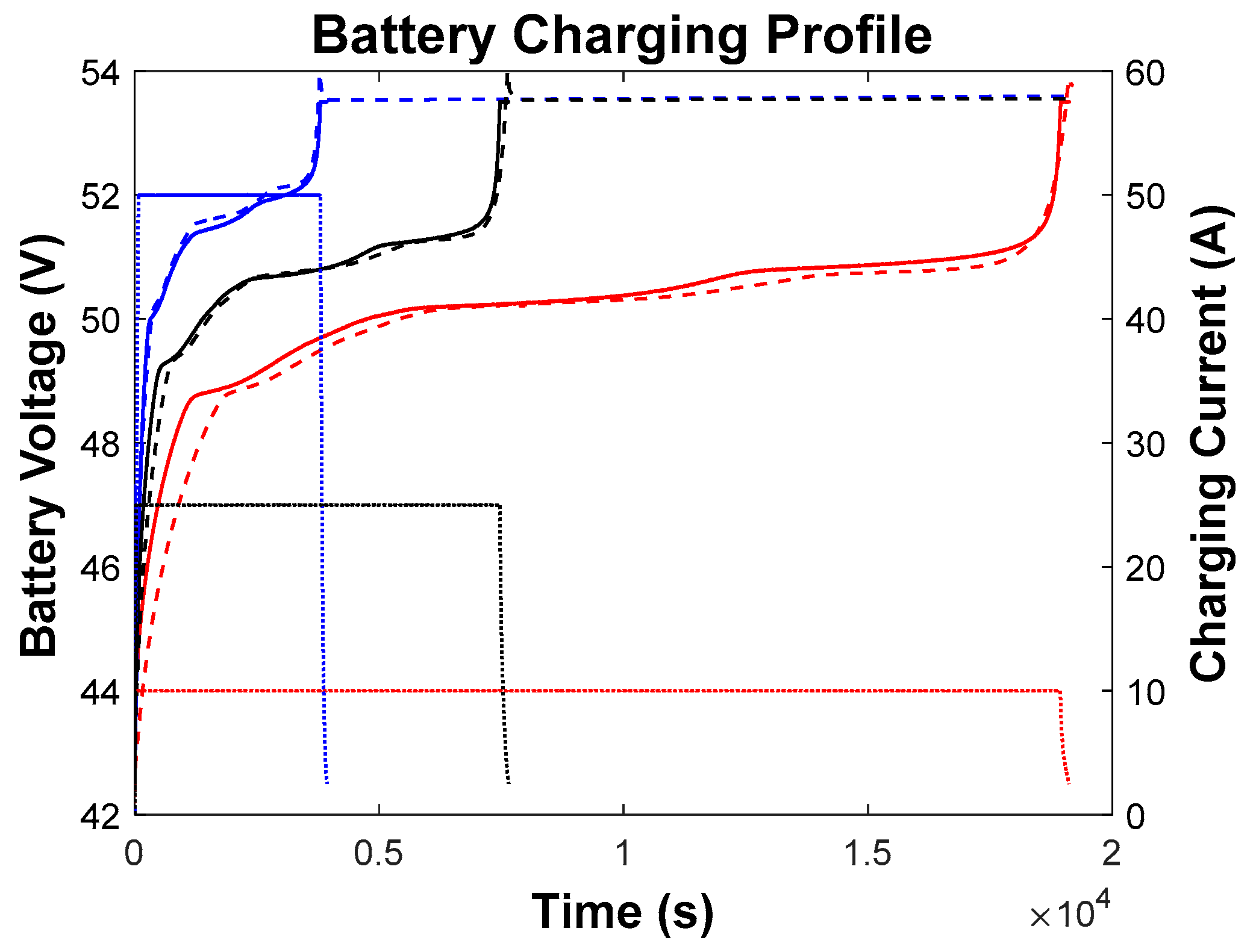
8. Results of the Experimental Prototype

An experimental prototype, shown in Figure 14, has been built to validate the theoretical proposal.
When connecting the battery to the charger, an initial frequency sweep is programmed to ensuring the gradual growth of the charging current to prevent the occurrence of an overvoltage across the discharged battery. The experimental waveforms in different circuit sections are shown in Figure 15, Figure 16 and Figure 17. In order to demonstrate the charger performance at different operation points, the waveforms for full load and 70% of full load operation are shown. In Figure 15, it is observed that the resonant current has a phase lag with respect to the input voltage. At full load condition, φi1,2 = φi3,4 = 54°, which is in good agreement with the theoretical value, and at 70% of the full load condition, φi1,2 = 54°, φi3,4 = 72°. The ZVS mode operation was verified for all phases of the resonant inverter section.
In Figure 16, the current and voltage at the primary side of the transformer are shown. The amplitude of the current square waveform is half (10 A) of the battery charging current. In Figure 17, the charging current at full load (20 A) and at 70% of full load are shown. The results are in good agreement with the theoretical value according to the control angle Ψ. It can be observed that the charging current ripple is negligible as it is required for this application. The experimental efficiency of the prototype measured at the point of maximum load (IBat = 20 A, PBat = 1.07 kW) was η = 91.3%. The efficiency at 70% and 50% of the full load was η = 90.2% and η = 88%, respectively. The experimental efficiency is slightly lower than the theoretical due to the switching losses, the power dissipation at the transistors drive circuit, and the auxiliary power supply loss.

9. Discussion

In this work, the general design method of the proposed charger has been explained, but the particular configuration of the final solution depends on the chosen technology. One key decision is the most suitable value of the dc-link voltage. The solution for an dc-link voltage Vdc = 400 V, which was obtained from a single-phase power factor corrector (PFC) based on a Boost Converter, and using the CoolMOSTM SPA11N60C3 MOSFET transistor and the STPS30M60S Schottky diode has been fully developed. As alternative, a solution with Vdc = 800 V, obtained from a three-phase PFC and using silicon carbide (SiC) components is also assessed. For this case, the third-generation C3M0065100K MOSFET transistor (Wolfspeed, Research Triangle Park, USA) with the CGD15SG00D2 driver (Wolfspeed, Research Triangle Park, USA) is used in the inverter section. As the voltage, current, and power at the circuit output are the same, the silicon (Si) Schottky diode STPS30M60S is used in both cases. For a better comparison, both designs are summarized in Table 2.
As it can be seen in Table 2, both designs achieve a similar theoretical efficiency, but the SiC technology uses only two phases for the resonant inverter stage.

Considerations about the Solution Cost

SiC technology for power devices is becoming more competitive in technical performance and cost. Important advances have been reported in terms of increasing the wafer diameter and minimization of the defect density [36], which contribute to lowering the cost of the devices, so it is worth comparing the cost of the proposed alternatives. Focusing on the inverter section of the described designs, i.e., Vdc = 400 V for the four-phase Si inverter and Vdc = 800 V for the two-phase SiC inverter, the cost assessment reveals that at present, the solution based on SiC components is more expensive despite requiring fewer transistors. The cost of the third-generation SiC MOSFET C3M0065100K is five times (5 ×) that of the SPA11N60C3 Si MOSFET. On the other hand, in contrast to the simplicity of the half-bridge driver, based on the integrated circuit IR2111, the complexity and cost of the selected driver CGD15SG00D2 for SiC MOSFETS are also significantly higher [37]. In addition, the PFC section adds a cost difference in favor of the Vdc = 400 V four-phase Si design. For illustrating the analysis, in Table 3 and Table 4, the cost of the SiC components and its Si counterparts are summarized [38]. Differences in the magnetic elements, capacitors, and control circuit have less impact on cost.
Nowadays, for a given architecture, the use of SiC MOSFETs could be recommended if the maximum current, voltage, and temperature limits of the Si MOSFETs are compromised, e.g., for charging currents and powers higher than 50 A and 2.5 kW, respectively.

10. Conclusions

The general design procedure of a multiphase resonant converter for battery charger applications has been presented. Since the output current on the AC side is shared among N equal inverter sections, the circuit presents high output current capability using low-cost power MOSFETs, and the design of the resonant inductors is simplified. The proposed output rectifier is based on an M-winding current-doubler rectifier that also diminishes the conduction loss by using passive components. The efficiency curve of the proposed charger exhibits a wide flat zone, assuring a constant value of efficiency even at light load conditions. This feature is very interesting for the battery charger applications, taking into account that high efficiency is desirable along the whole charging process, despite the heavy load variation. The effect on the AC side of the leakage inductance of the transformer Lk is canceled out by the series capacitor Cs. The maximum charging current is limited by the circuit in an inherent manner, without the necessity of any control. However, the output voltage is limited to the maximum value recommended for the battery by a voltage control loop with a type I error amplifier. The control action is performed keeping constant the switching frequency by adjusting the control angle, Ψ, while maintaining the ZVS mode at any operation point. The general proposal has been validated by implementing an experimental prototype for charging a commercial 48 V LiFePO4 battery with 50 Ah of capacity. The achieved efficiency of the N = 4 inverter with Vdc = 400 V using Si MOSFETs is similar to the predicted with an N = 2 inverter with Vdc = 800 V using SiC MOSFETs.

Author Contributions

The battery characterization and the experimental evaluation of the different charging profiles were carried out at the Batteries Laboratory of University of the Oviedo by J.C.V. and M.G. The proposed charger was developed at the Power Electronics Laboratory of the University of Cantabria by C.B., F.J.A., R.C. and F.J.D. Conceptualization, C.B. and J.C.V.; methodology, C.B. and J.C.V.; validation, C.B., J.C.V., R.C. and F.J.D.; formal analysis, C.B. and J.C.V.; investigation, C.B., J.C.V. and F.J.A.; writing—original draft preparation, C.B. and J.C.V.; writing—review and editing, F.J.A., M.G., R.C. and F.J.D.; project administration, F.J.A. and M.G.; funding acquisition, F.J.A. and M.G. All authors have read and agreed to the published version of the manuscript.

Funding

This work was funded by the Spanish Ministry of Science and the EU through the projects RTI2018-095138-B-C31: “Power Electronics for the Grid and Industry Applications”, TEC2016-80700-R (AEI/FEDER/UE), PID2019-110955RB-I00, and by the Principality of Asturias via Project FC-IDI/2018/000226.

Conflicts of Interest

The authors declare no conflict of interest.

References

  1. Khaligh, A.; Li, Z. Battery ultracapacitor, fuel cell, and hybrid energy storage systems for electric, hybrid electric, fuel cell, and plug-in hybrid electric vehicles: State of the art. IEEE Trans. Veh. Technol. 2010, 59, 2806–2814. [Google Scholar] [CrossRef]
  2. Braun, P.; Cho, J.; Pikul, J.; King, W.; Zhang, H. High power rechargeable batteries. Curr. Opin. Solid State Mater. Sci. 2012, 16, 186–198. [Google Scholar] [CrossRef]
  3. Waag, W.; Fleischer, C.; Sauer, D.U. Critical review of the methods for monitoring of lithium-ion batteries in electric and hybrid vehicles. J. Power Sources 2014, 258, 321–339. [Google Scholar] [CrossRef]
  4. Wei, Z.; Zhao, J.; Xiong, R.; Dong, G.; Pou, J.; Tseng, K.J. Online Estimation of Power Capacity With Noise Effect Attenuation for Lithium-Ion Battery. IEEE Trans. Ind. Electron. 2019, 66, 5724–5735. [Google Scholar] [CrossRef]
  5. Wei, Z.; Zhao, D.; He, H.; Cao, W.; Dong, G. noise-tolerant model parameterization method for lithium-ion battery management system. Appl. Energy 2020, 268, 114932. [Google Scholar] [CrossRef]
  6. Ke, M.Y.; Chiu, Y.H.; Wu, C.Y. Battery Modelling and SOC Estimation of a LiFePO4 Battery. In Proceedings of the 2016 International Symposium on Computer, Consumer and Control (IS3C), Xi’an, China, 4–6 July 2016. [Google Scholar]
  7. Wang, A.; Jin, X.; Li, Y.; Li, N. LiFePO4 battery modeling and SOC estimation algorithm. In Proceedings of the 2017 29th Chinese Control and Decision Conference (CCDC), Chongqing, China, 28–30 May 2017. [Google Scholar]
  8. Kazimierczuk, M.K.; Czarkowski, D. Resonant Power Converters, 2nd ed.; John Wiley & Sons: Hoboken, NJ, USA, 2012. [Google Scholar]
  9. Lin, C.H.; Wang, C.M.; Hung, M.H.; Li, M.H. Series-resonant battery charger with synchronous rectifiers for LiFePO4 battery pack. In Proceedings of the 2011 6th IEEE Conference on Industrial Electronics and Applications, Beijing, China, 21–23 June 2011. [Google Scholar]
  10. Karimi, S.; Tahami, F. A Comprehensive Time-domain-based Optimization of a High-Frequency LLC-based Li-ion Battery Charger. In Proceedings of the 2019 10th International Power Electronics, Drive Systems and Technologies Conference (PEDSTC), Shiraz, Iran, 12–14 February 2019. [Google Scholar]
  11. Shafiei, N.; Ordonez, M.; Craciun, M.; Botting, C.; Edington, M. Burst Mode Elimination in High-Power LLC Resonant Battery Charger for Electric Vehicles. IEEE Trans. Power Electron. 2016, 31, 1173–1188. [Google Scholar] [CrossRef]
  12. Park, S.M.; Kim, D.H.; Joo, D.M.; Kim, M.J.; Lee, B.K. Design of Output Filter in LLC Resonant Converters for Ripple Current Reduction in Battery Charging Applications. In Proceedings of the 9th International Conference on Power Electronics-ECCE Asia, Seoul, Korea, 1–5 June 2015. [Google Scholar]
  13. Liu, X.; Baguley, C.A.; Madawala, U.K.; Thrimawithana, D.J. A Compact Power Converter for High Current and Low Voltage Applications. In Proceedings of the 39th Annual Conference of the IEEE Industrial Electronics Society, Vienna, Austria, 10–13 November 2013; pp. 140–144. [Google Scholar]
  14. Yilmaz, M.; Krein, P.T. Review of battery charger topologies, charging power levels, and infrastructure for plug-in electric and hybrid vehicles. IEEE Trans. Power Electron. 2013, 28, 2151–2169. [Google Scholar] [CrossRef]
  15. Ashok, B. Wide-Bandgap-Based Power Devices. IEEE Power Electron. Mag. 2015, 2, 42–47. [Google Scholar]
  16. Branas, C.; Azcondo, F.J.; Casanueva, R. A Generalize Study of Multiphase Parallel Resonant Inverters for High-Power Applications. IEEE Trans. Circuits Syst. 2008, 55, 2128–2138. [Google Scholar] [CrossRef]
  17. Narada NPFC Series. Operation Manual. Available online: https://mpinarada.com/wp-content/uploads/2019/01/OM-Narada-NPFC-Series-Li-Ion-0423-V8.pdf (accessed on 22 January 2021).
  18. Keil, P.; Jossen, A. Charging protocols for lithium-ion batteries and their impact on cycle life—An experimental study with different 18650 high-power cells. J. Energy Storage 2016, 6, 125–141. [Google Scholar] [CrossRef]
  19. Wu, J.; Wei, Z.; Liu, K.; Quan, Z.; Li, Y. Battery-Involved Energy Management for Hybrid Electric Bus Based on Expert-Assistance Deep Deterministic Policy Gradient Algorithm. IEEE Trans. Veh. Technol. 2020, 69, 12786–12796. [Google Scholar] [CrossRef]
  20. Wu, J.; Wei, Z.; Li, W.; Wang, Y.; Li, Y.; Sauer, D. Battery Thermal- and Health-Constrained Energy Management for Hybrid Electric Bus based on Soft Actor-Critic DRL Algorithm. IEEE Trans. Ind. Inform. 2020. [Google Scholar] [CrossRef]
  21. Notten, P.H.; het Veld, J.O.; Van Beek, J.R.G. Boostcharging Li-ion batteries: A challenging new charging concept. J. Power Sources 2005, 145, 89–94. [Google Scholar] [CrossRef]
  22. Perez, H.E.; Dey, S.; Hu, X.; Moura, S.J. Optimal Charging of Li-Ion Batteries via a Single Particle Model with Electrolyte and Thermal Dynamics. J. Electrochem. Soc. 2017, 164, 1–10. [Google Scholar] [CrossRef]
  23. Anseán, D.; González, M.; Viera, J.C.; García, V.M.; Blanco, C.; Valledor, M. Fast charging technique for high power lithium iron phosphate batteries: A cycle life analysis. J. Power Sources 2013, 239, 9–15. [Google Scholar] [CrossRef]
  24. Anseán, D.; Dubarry, M.; Devie, A.; Liaw, B.Y.; García, V.M.; Viera, J.C.; González, M. Fast charging technique for high power LiFePO4 batteries: A mechanistic analysis of aging. J. Power Sources 2016, 321, 201–209. [Google Scholar] [CrossRef]
  25. Chen, M.; Rincon-Mora, G.A. Accurate Electrical Battery Model Capable of Predicting Runtime and I-V Performance. IEEE Trans. Energy Convers. 2006, 21, 504–511. [Google Scholar] [CrossRef]
  26. Truchot, C.; Dubarry, M.; Liaw, B.Y. State-of-charge estimation and uncertainty for lithium-ion battery strings. Appl. Energy 2014, 119, 218–227. [Google Scholar] [CrossRef]
  27. Jossen, A. Fundamentals of battery dynamics. J. Power Sources 2006, 154, 530–538. [Google Scholar] [CrossRef]
  28. Bojarski, M.; Asa, E.; Colak, K.; Czarkowski, D. A 25 kW Industrial Prototype Wireless Electric Vehicle Charger. In Proceedings of the 2016 IEEE Applied Power Electronics Conference and Exposition (APEC), Long Beach, CA, USA, 20–24 March 2016; pp. 1756–1761. [Google Scholar]
  29. Erickson, R.W.; Maksimovic, D. Fundamentals of Power Electronics, 2nd ed.; Springer: New York, NY, USA, 2001. [Google Scholar]
  30. Zhang, J.; Hurley, W.G.; Wölfle, W.H. Gapped Transformer Design Methodology and Implementation for LLC Resonant Converters. IEEE Trans. Ind. Appl. 2016, 52, 342–350. [Google Scholar] [CrossRef]
  31. Huber, L.; Jovanovic, M.H. Forward-flyback Converter with Current-Doubler Rectifier: Analysis, Design and Evaluation Results. IEEE Trans. Power Electron. 1999, 14, 184–192. [Google Scholar] [CrossRef] [Green Version]
  32. Alou, P.; Oliver, J.A.; García, O.; Prieto, R.; Cobos, J.A. Comparison of Current Doubler Rectifier and Center Tapped Rectifier for Low Voltage Applications. In Proceedings of the Twenty-First Annual IEEE Applied Power Electronics Conference and Exposition, (APEC’06), Dallas, TX, USA, 19–23 March 2006; pp. 744–750. [Google Scholar]
  33. Lopez, V.M.; Navarro-Crespin, A.; Schnell, R.W.; Branas, C.; Azcondo, F.J.; Zane, R. Current Phase Surveillance in Resonant Converters for Electric Discharge Applications to Assure Operation in Zero-Voltage-Switching Mode. IEEE Trans. Power Electron. 2012, 27, 2925–2935. [Google Scholar] [CrossRef]
  34. Plett, G. Extended Kalman Filtering for Battery Management System of LiPB-Based HEV Battery Packs—Part 1: Background. J. Power Sources 2004, 134, 252–261. [Google Scholar] [CrossRef]
  35. Plett, G. Extended Kalman Filtering for Battery Management Systems of LiPb-Based HEV Battery Packs—Part 2: Modeling and Identification. J. Power Sources 2004, 134, 262–276. [Google Scholar] [CrossRef]
  36. Loboda, M.J.; Chung, G.; Carlson, E.; Drachev, R.; Hansen, D.; Sanchez, E.; Wan, J.; Zhang, J. Advances in SiC Substrates for Power and Energy Applications. In Proceedings of the GOMACTECH Conference, Palm Springs, CA, USA, 16–19 May 2011. [Google Scholar]
  37. Hazra, S.; Vechalapu, K.; Madhusoodhanan, S.; Bhattacharya, S.; Hatua, K. Gate Driver Design Considerations for SiliconCarbide MOSFETs Including For Series Connected Devices. In Proceedings of the 2017 IEEE Energy Conversion Congress and Exposition (ECCE), Cincinnati, OH, USA, 1–5 October 2017. [Google Scholar]
  38. Nielsen, R.Ø.; Török, L.; Munk-Nielsen, S.; Blaabjerg, F. Efficiency and Cost Comparison of Si IGBT and SiC JFET Isolated DC/DC Converters. In Proceedings of the IECON 2013—39th Annual Conference of the IEEE Industrial Electronics Society, Vienna, Austria, 10–13 November 2013. [Google Scholar]
Figure 1. (Left) Laboratory facility for battery testing. (Right) Battery connected to SBT-10050 test equipment.
Electronics 10 00266 g001
Figure 2. Experimental charging profiles at 10, 25, and 50 A for a 48NPFC50 LiFePO4 battery.
Electronics 10 00266 g002
Figure 3. Battery model considering Ns stacked cells in series.
Electronics 10 00266 g003
Figure 4. Quasi-open-circuit voltage of the cell as a function of the state of charge (SOC) obtained at Cn/50 for a complete charge/discharge cycle. Solid line: Charge trajectory. Dashed line: Discharge trajectory.
Electronics 10 00266 g004
Figure 5. General architecture of the battery charger based on an N-phase LCpCs resonant inverter with an M-winding current-doubler rectifier as output stage. Multiple configurations are possible according to the N and M values.
Electronics 10 00266 g005
Figure 6. Output voltages of each inverter section obtained in the midpoint of the transistors leg.
Electronics 10 00266 g006
Figure 7. Simplified model using the fundamental approximation for circuit analysis purposes of the inverter stage.
Electronics 10 00266 g007
Figure 8. (Left) Current-doubler rectifier considering the positive semi-cycle of the drive voltage vac. (Right) Theoretical voltage waveform at the filter inductors.
Electronics 10 00266 g008
Figure 9. Amplitude of the normalized charging current, IBat, as a function of the control angle, Ψ, for N = 2, 3, and 4. All phases are evenly shifted, Ψ0 = 0°, Ψ1 = Ψ, Ψ2 = 2Ψ, …, ΨN−1 = (N–1)Ψ.
Electronics 10 00266 g009
Figure 10. Maximum efficiency of the resonant inverter stage, ηI(Max), and efficiency of the output current multiplier, ηR, as a function of the number of phases, N, and secondary windings M. The following typical values are assumed: n = 2, r = 1.7 Ω, IBat(Max) = 20 A, 2rIBat(Max)2VBat(Max) = 0.5, VD/VBat(Max) = 0.05 and rD = rLF = 0.1.
Electronics 10 00266 g010
Figure 11. Control loop for limiting the maximum battery voltage, VBat(Max).
Electronics 10 00266 g011
Figure 12. Simulink® model of the battery.
Electronics 10 00266 g012
Figure 13. Charging profiles at 10, 25, and 50 A. Solid lines: Experimental battery voltage. Dashed lines: Simulation result. Dot lines: Charging current.
Electronics 10 00266 g013
Figure 14. Details of the experimental prototype of the charger. (Left) Four-phase resonant inverter stage. (Right) Current-doubler rectifier.
Electronics 10 00266 g014
Figure 15. From top to bottom: Midpoint voltages of phases 1 and 2, v1,2. Midpoint voltages of phases 3 and 4, v3,4. Resonant current of phases 1 and 2, i1,2. Resonant current of phases 3 and 4, i3,4. (Left) Full load condition (Ψ0 = Ψ1 = Ψ2 = Ψ3 = 0°). (Right) 70% of full load condition (Ψ0 = Ψ1 = 0°, Ψ2 = Ψ3 = 90°).
Electronics 10 00266 g015
Figure 16. From top to bottom: Output current through the primary side of the transformer, iac. Output voltage applied to the primary side of the transformer, vac. (Left) Full load condition (Ψ0 = Ψ1 = Ψ2 = Ψ3 = 0°). (Right) 70% of full load condition (Ψ0 = Ψ1 = 0°, Ψ2 = Ψ3 = 90°).
Electronics 10 00266 g016
Figure 17. From top to bottom: Midpoint voltages of phases 1 and 2, v1,2. Midpoint voltages of phases 3 and 4, v3,4. Charging current iBat. (Left) Full load condition (Ψ0 = Ψ1 = Ψ2 = Ψ3 = 0°). (Right) 70% of full load condition (Ψ0 = Ψ1 = 0°, Ψ2 = Ψ3 = 90°).
Electronics 10 00266 g017
Table 1. Parameters of the LCpCs resonant inverter.
Parallel Resonant FrequencyParallel Characteristic ImpedanceParallel Quality Factor
ω p = 1 L C p / N Z p = ω p L = N ω p C p Q p = N R a c Z p
Table 2. Designs comparison.
VdcnNMZpQpNηIBat(Max)PBat(Max)
400 V14180 Ω0.6240.9520 A1.07 kW
800 V221160 Ω0.6240.96620 A1.07 kW
Table 3. SiC resonant inverter.
ComponentQuantityCost
(Retail Sale)
MOSFET
C3M0065100K
440€
Driver
CGD15SG00D2
4200€
Table 4. Si resonant inverter.
ComponentQuantityCost
(Retail Sale)
MOSFET
SPA11N60C3
816€
Driver
IR2111
48€
Publisher’s Note: MDPI stays neutral with regard to jurisdictional claims in published maps and institutional affiliations.

