Article

Compact, Reflectionless Band-Pass Filter: Based on GaAs IPD Process for Highly Reliable Communication

1
School of Information Engineering, Kunming University, Kunming 650214, China
2
Yangtze Delta Region Institute, University of Electronic Science and Technology of China, Huzhou 313001, China
3
School of Electronic Information, Wuhan University, Wuhan 430072, China
4
School of Microelectronics, Tianjin University, Tianjin 300072, China
5
Yunnan Collegiate Key Laboratory for Data Governance and Intelligent Decision, Kunming 650214, China
*
Author to whom correspondence should be addressed.
Electronics 2021, 10(23), 2998; https://doi.org/10.3390/electronics10232998
Submission received: 1 November 2021 / Revised: 25 November 2021 / Accepted: 25 November 2021 / Published: 1 December 2021
(This article belongs to the Section Microwave and Wireless Communications)

Abstract

:
For highly reliable and compact communication of front-end modules, a miniaturized reflectionless band-pass filter, based on the GaAs integrated passive device (IPD) process, is proposed in this work. The stop-band signal absorption rate of the filter can reach more than 90% and greatly reduce the influence of electromagnetic interference for sensitive devices. First, a circuit topology of reflectionless filter is proposed. Then, the miniaturized reflectionless band-pass filter is designed and fabricated based on GaAs IPD process with a compact size of only 0.85 mm × 1.33 mm × 0.09 mm (0.011λ × 0.018λ × 0.001λ). The filter operates at frequency ranging from 3.3 GHz to 4.5 GHz for 5G communication, the insertion loss (S21) is less than 3 dB, the return loss in the passband (S11) is over 15 dB, the stopband return loss (S11) is over 10 dB, and the out-of-band suppression (S21) reached 19 dB. All the measured results are in good agreement with the simulated results. It shows great potential in the process of designing highly reliable and compact monolithic integrated wireless modules and wearable electronics.

1. Introduction

A filter, as an important component in the front-end modules of wireless communication equipment, selectively pass and filter the signals in the frequency spectrum according to the different working frequency bands. Most filters have the type of reflection for stopband signals, meaning that the useless stopband signal is reflected back to the source port, which is the way that filters normally work [1,2,3]. However, the reflected stopband signal may bring negative impact on the performance of the previous stage in front-end modules or even affect the whole wireless communication system [4,5,6,7,8]. For instance, the filter is always added between the amplifier and analog-to-digital converter (ADC) for filtering processing, and the useless stopband signal, reflected by filter, may be resampled by the ADC, thus reducing the spurious free dynamic range (SFDR) of the ADC [5]. Besides that, in a solid-state transmitter, the homomorphic power amplifier usually has poor suppression of harmonic waves, and the output of the amplifier contains a large number of second and third harmonic waves. These harmonic waves in the stopband are reflected back to the power amplifier by the filter, which may affect the normal work of the power amplifier, or even cause the power amplifier to burn [8]. Attenuators can be used for solving these problems; however, more chip footprint and large insertion loss are introduced, which seriously affects the development of miniaturized monolithic integrated circuits [9].
Morgan firstly proposed the reflectionless filter in 2011, when he deduced the topology prototype of the first reflectionless filter, based on the two-port network [5]. The drawback of the low, out-of-band suppression of the reflectionless filter was also analyzed, which can only reach 14.47 dB. By cascading multiple reflectionless filters, the out-of-band suppression was increased to 42 dB, but the number of components was doubled. An ultra-wideband reflectionless band-pass filter was proposed by combining a cascading, reflectionless low-pass filter and reflectionless high-pass filter, which works at center frequency of 6 GHz, with a return loss of less than 10 dB in both passband and stopband, and an out-of-band suppression that only reached 10 dB [7]. In [10], a reflectionless inverse Chebyshev filter structure with arbitrary attenuation is proposed, and a low-pass filter with a cutoff frequency of 70 MHz is designed to verify their design concept. In [11], a band-pass filter, based on surface acoustic wave (SAW) is designed and measured at 418 MHz using conventional SAW. The reflectionless filters given in [10,11,12] are designed based on lumped elements; however, they are applied or verified at lower frequencies (~hundreds of MHz) and most of them are stop-band filters [13,14,15,16,17,18]. In the past decade, simplifying the topology prototype of reflectionless filter was pursued as an important goal to realize miniatured reflectionless filter [10,11,12,19,20,21,22] and filters applied for high frequency communication are desirable.
In this paper, a highly reliable and compact reflectionless band-pass filter, based on the GaAs integrated passive device (IPD) process, is proposed. A circuit topology of a reflectionless filter is proposed and the miniaturized reflectionless band-pass filter is designed and fabricated, based on GaAs IPD process with compact size of only 0.85 mm × 1.33 mm × 0.09 mm (0.011λ × 0.018λ × 0.001λ). The insertion loss (S21) is less than 3 dB, the return loss in the passband (S11) is over 15 dB, the stopband return loss (S11) is over 10 dB, and the out-of-band suppression (S21) reached 19 dB. The stop-band signal absorption rate of the filter can reach more than 90% and greatly reduce the influence of electromagnetic interference for sensitive devices. All the measured results are in good agreement with the simulated results. It shows great potential in designing of highly reliable and compact monolithic integrated wireless modules and wearable electronics.

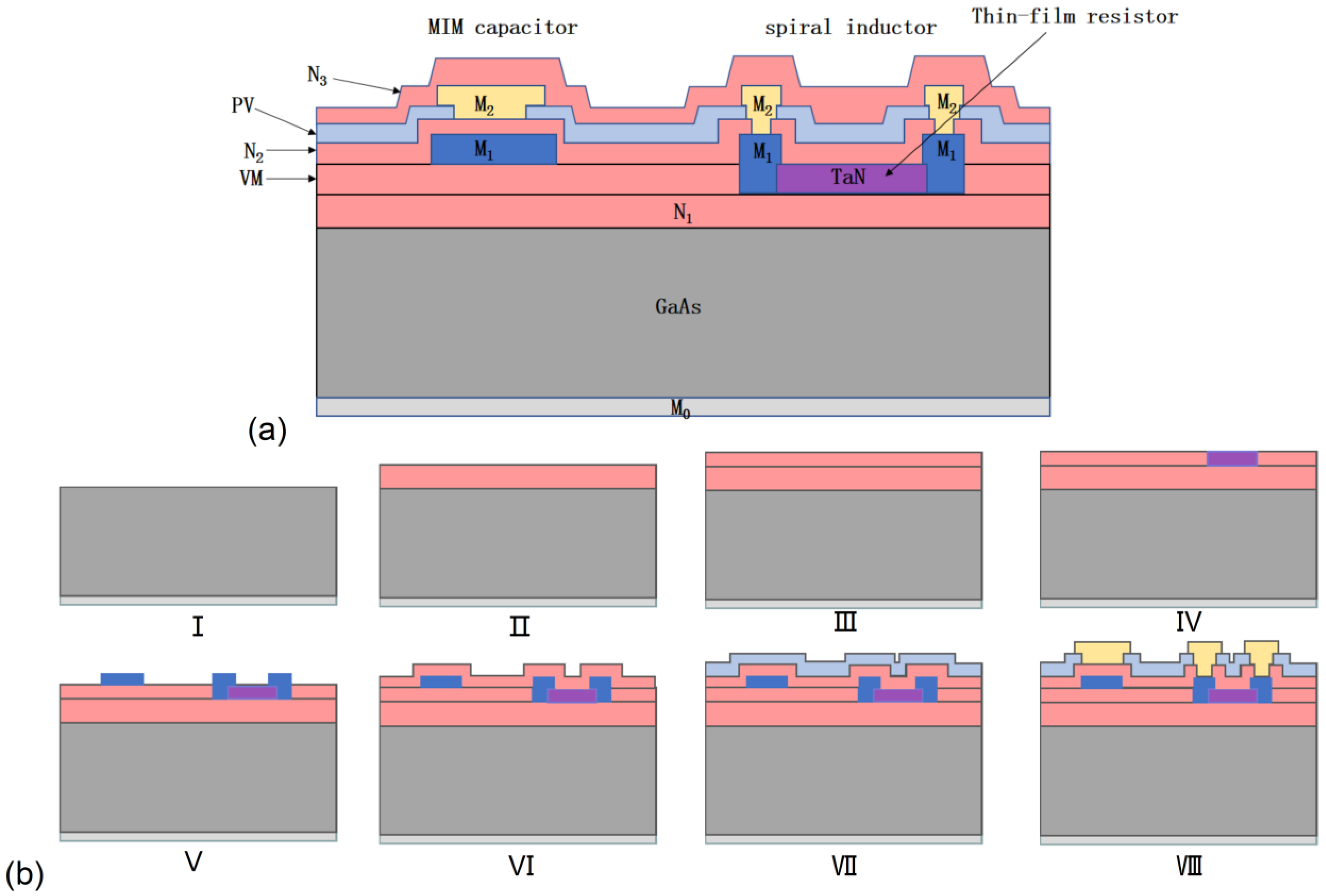
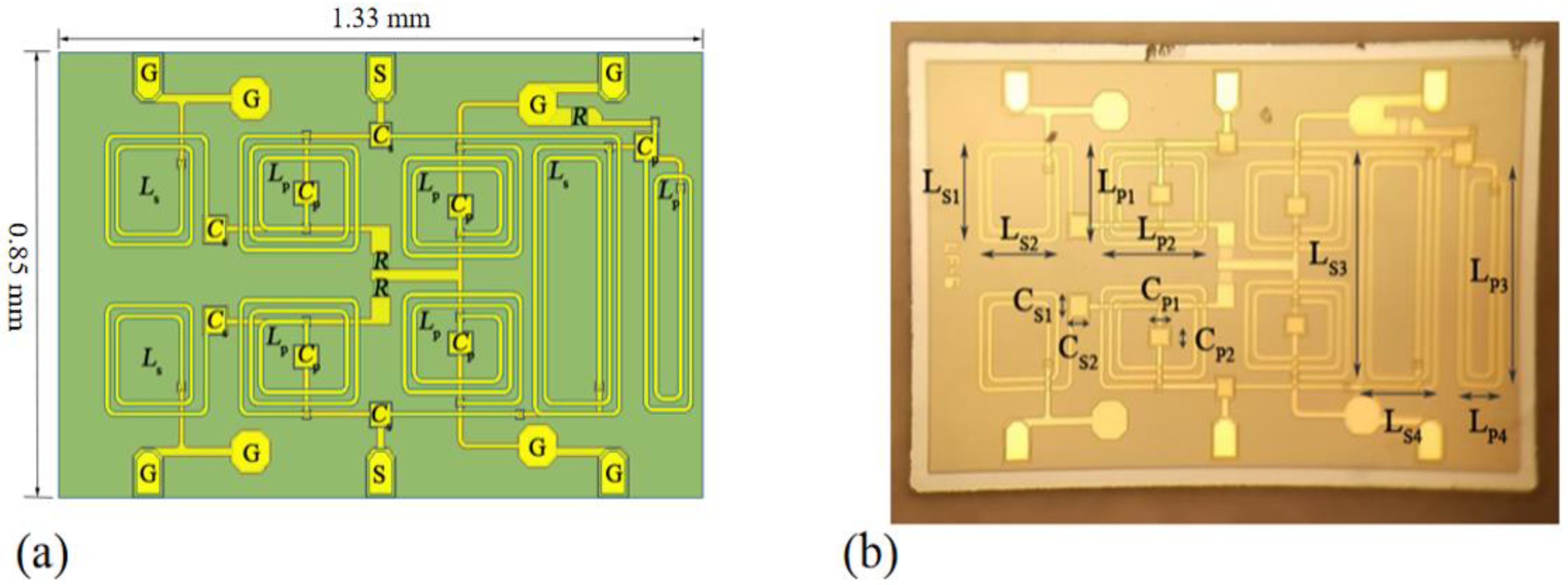
2. Circuit Design and Fabrication Process

A circuit topology of reflectionless band-pass filter is proposed by using the method of transforming low-pass filter into band-pass filter. As shown in Figure 1a, the circuit topology of the reflectionless low-pass filter is presented. For the convenience of design and research, the symmetry of the reflectionless filter is retained, and all the inductance and capacitance values maintained the same symmetricity [4]. The circuit topology in Figure 1a (excluding the unit ➀) can be regarded as an odd-mode and even-mode equivalent circuit [5], and it is obtained that:
Γ even = Z even 1 Z even 1 = s 2 + 1 2 s 3 + 3 s 2 + 2 s + 1
Γ odd = Z odd 1 Z odd + 1 = s 2 1 2 s 3 + 3 s 2 + 2 s + 1
where S was complex number variable, which transformed microwave transmission signal into complex frequency domain for more flexible computing and derivation. Γeven and Γodd represent the reflection coefficient of even and odd mode equivalent circuits, respectively, Zeven and Zodd represent the impedance of even and odd mode equivalent circuits, respectively. It can be obtained from Equations (1) and (2), that
S 11 = S 22 = 1 2 ( Γ even + Γ odd ) = 0
From Equation (3), the low-pass filter can show the 100% absorption performance, and the validity of the reflectionless circuit is verified.
The frequency transformation from the reflectionless low-pass filter to the band-pass filter is deduced as follows. The transformed third-order reflectionless band-pass filter is shown in Figure 1b. Frequency transformed from reflectionless low-pass filter to reflectionless band-pass filter is as follows:
ω ω c 1 Δ ( ω ω 0 ω 0 ω )
Δ = ω 2 ω 1 ω 0
ω 0 = ω 1 ω 2
where ω1 and ω2 are the upper and lower limits of the cut-off frequency of the band-pass filter, and ωc is the cut-off frequency of the low-pass filter. Considerate of normalized coefficient gk, the low-pass filter with inductance reactance of gkZ0ω/ωc can be transformed in inductance reactance of Z0ω/ω0Δ-gkZ0ω0/ωΔ for band-pass filter, which can be considered as series connection of inductance and capacitor. Similarly, the capacitance in a low-pass filter is equivalent to the shunt connection of the inductance and capacitance in a band-pass filter [22].
Table 1 lists the frequency conversions of the reflectionless low-pass filter to band-pass filter. In Table 1, Ls and Cs, respectively, represent the series inductance and capacitance in reflectionless band-pass filter; Lp and Cp, respectively, represent the shunt inductance and capacitance in reflectionless band-pass filter. Normalized coefficient gk can be determined by cut-off frequency of the upper and lower limits of the proposed band-pass filter, which is deduced as follows:
The transfer function of the inverse Chebyshev filter is given, as shown in Equation (7), as follows:
| H ( j ω ) | = 1 1 + ε 2 T N 2 ( ω 1 )
where ε is the ripple factor with a value of 0.1925, and TN is the N-order Chebyshev polynomial [21].
| H ( j ω I L ) | 2 = 1 + ε 2 T N 2 ( ω I L 1 ) = 10 I L / 10
T N ( ω I L 1 ) = cosh ( N cosh 1 ( ω I L 1 ) ) = 1 ε 10 I L / 10 1
ω I L 1 = cosh ( 1 N cosh 1 ( 1 ε 10 I L / 10 1 ) )
where ωIL represents the frequency at the specified insertion loss (i.e., IL = 3 dB in this work). For IL = 3 dB, gk must be multiplied by the appropriate relative offset α = 31/2/2 [22], so that:
g k = α ω I L
Figure 2a shows the stacks of IPD process on the GaAs substrate with thickness of 75.75 µm. A series of multi-layer structures such as metal, dielectric, and through holes, etc., are fabricated on the substrate to form MiM (metal–insulator–metal) capacitor, high-Q value spiral inductor, and thin-film resistor. Figure 2b shows major fabrication steps of GaAs IPD process for fabrication of reflectionless band-pass filter. Three layers of electroplated gold M0, M1 and M2 are contained in this structure, where M0 is used for ground connection and M1 and M2 layers are used for upper and lower plates of the MIM capacitor, spiral inductor, and routing connection. N1 is the first layer of Si3N4 with thickness of 0.16 μm, which sets the position of pad and through hole. The thickness of the VM layer is 1.3 μm, which provides the film protection with Si3N4 passivation, and provides a protective ring around the capacitor. N2 is a layer of Si3N4 with thickness of 0.1 μm, which acts as the dielectric layer of MIM capacitor. PV is a layer of polyimide with thickness of 1.6 μm and serves as the packed dielectric between the M1 and M2 layers to reduce cross capacitance. N3 is 4.8 μm-thick Si3N4 and provides the final Si3N4 layer for passivation of the device.

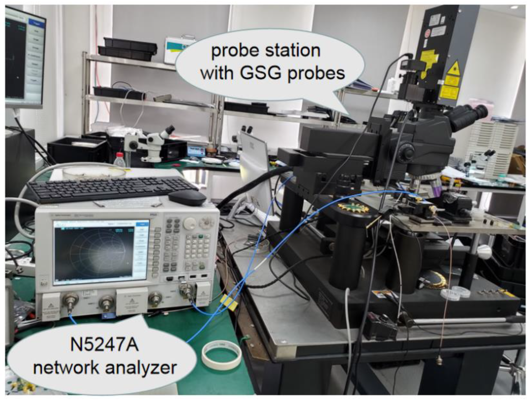
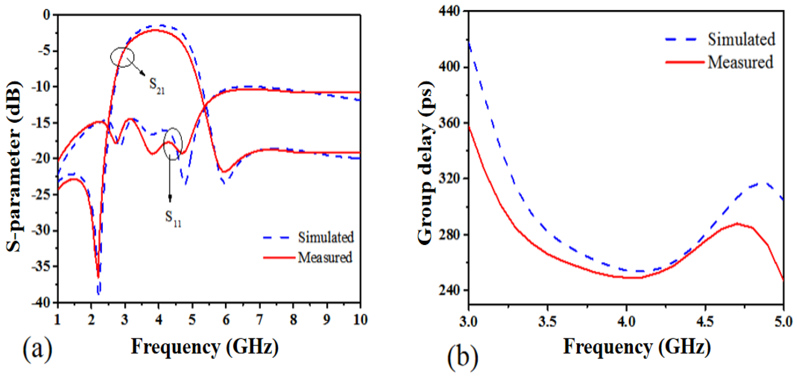
3. Results and Discussion

In this work, a reflectionless band-pass filter, which has upper and lower limits of 3.3 GHz and 4.5 GHz (i.e., 3 dB bandwidth) of the cut-off frequency of the band-pass filter, respectively. Based on the above parameters, derivation, and the description in Table 1, the component values can be calculated as: gk = 0.6573, LS = 4.36 nH, CS = 0.38 pF, LP = 0.96 pF, CP = 1.74 nH.
Based on the IPD process schematic, as shown in Figure 2, the electromagnetic field model of the 5G reflectionless band-pass filter is designed with FEM simulated software HFSS. The model of the filter is shown in Figure 3a, the layout of the inductor, capacitor, resistor, and ground–signal–ground (GSG) pads are marked. Figure 3b shows the fabricated reflectionless band-pass filter based on GaAs IPD process. The dimensions of each inductor and capacitor are marked and shown in Table 2. The physical size of the proposed reflectionless band-pass filter is only 0.85 mm × 1.33 mm × 0.09 mm. The filter is measured using a vector network analyzer (Keysight PNA N5247A) with on-wafer GSG probes, as shown in Figure 4.
The simulated results are shown in Figure 5a with dash line and show that the bandwidth of the filter is 1.2 GHz (i.e., 3.3–4.5 GHz) with insertion loss less than 3 dB, the insertion loss of central frequency is 1.8 dB, the stopband return loss is more than 10 dB, and out-of-band suppression is greater than 23 dB. As the stopband return loss S11= −20 log|S11| = −20 log|Γ| > 10 dB, the reflection coefficient |Γ| < 1/3, which suggests that the absorption rate of the reflected signal reaches 90%, and only 10% is reflected. The good absorption characteristics and high suppression characteristics of this band-pass filter are initially verified. Additionally, the squareness factor (SF) was presented for describing the selectivity of filter by following equation:
S F = B W 20 dB B W 3 dB
where BW20dB and BW3dB were the bandwidths of filters within the range of 3 dB and 20 dB. SF was calculated as 2.08 for the filter in this paper.
As can be seen from Figure 5a, the measured S-parameter result shows that in the 3.3 GHz–4.5 GHz frequency band, the insertion loss of filter is less than 3 dB, the minimum insertion loss is 3.9 GHz and 2.1 dB, the in-band return loss is more than 15 dB, and the out-of-band suppression is more than 19 dB. The relative bandwidth is up to 30.8%, and the out-of-band return loss is more than 10 dB. Except the S-parameter, the measured group delay is also shown in Figure 5b, where the in-band group delay of the proposed filter is 250–280 ps, and the group delay fluctuation is only 30 ps, showing a good phase response. In summary, the measured results of the reflectionless filter are in good agreement with the simulated results, and the slight deviation is mainly due to the error brought by the test environment. Hence, the accuracy of the circuit topology, the GaAs IPD process model, and the good reflectionless characteristics of the band-pass filter are verified.
Table 3 lists various important performance indicators of proposed reflectionless band-pass filters. However, research of reflectionless band-pass filters are limited nowadays, especially by IPD process. The main forms of third-order, reflectionless band-pass filters were listed in Table 3. Symmetrical structure of band-pass filter was presented in reference [5]. The reflectionless band pass filter in Reference [6] was presented with the same symmetrical structure as that in [5], but the process was different. A cascaded reflectionless band-pass filter was presented in reference [7], which cascaded HPFs (high-pass filters) and LPFs (low-pass filters). The cascaded structure has the advantages of forming UWB (ultra-wide band) filter. In this paper, an absorption suppression unit (unit ➀ marked in Figure 1a) was added to the structure in [5] and [6], which improved the performance with fewer elements and was realized by the IPD process. From the comparison, the proposed reflectionless band-pass filter in this paper has obvious advantages in design method, layout size, component number, and high out-of-band suppression.

4. Conclusions

This paper proposes a circuit topology of the reflectionless band-pass filter, and the miniatured reflectionless band-pass filter is realized based on a GaAs IPD process with compact layout. The measured results show good agreement with the design parameters. The circuit topology of the reflectionless filter is versatile and is not limited to the working frequency mentioned in this paper, and can be used in a series of designs for applications in different signal bands. The research of the reflectionless filter points out a new idea for the design of passive filters with good performances and compact chip sizes for highly reliable communication in front-end modules.

Author Contributions

Conceptualization, X.L. and M.X.; Formal analysis, C.D.; Investigation, M.H.; Methodology, M.X.; Software, G.L.; Writing—original draft, X.Y.; Writing—review & editing, X.Y. All authors have read and agreed to the published version of the manuscript.

Funding

This research was funded by National Natural Science Foundation of China, grant number 61864004, 62066023, and also supported by the Tianjin Postgraduate Research and Innovation Project, grant number 2019YJSB189.

Conflicts of Interest

The authors declare no conflict of interest.

References

  1. Jiang, Y.; Tang, W.C.; Shi, Y.R.; Zhou, P.; Feng, L.P. Compact and low insertion loss UWB on-chip band-pass filter using coupled meandered line. Microw. Opt. Technol. Lett. 2020, 62, 2236–2242. [Google Scholar] [CrossRef]
  2. Kim, D.M.; Min, B.W.; Yook, J.M. Compact mm-wave band-pass filters using silicon integrated passive device technology. IEEE Microw. Wirel. Compon. Lett. 2019, 29, 638–640. [Google Scholar] [CrossRef]
  3. Shen, G.X.; Che, W.Q. Compact Ku-band LTCC band-pass filter using folded dual-composite right- and left-handed resonators. Electron. Lett. 2020, 56, 17–18. [Google Scholar] [CrossRef]
  4. Guilabert, A.; Morgan, M.A.; Boyd, T.A. Reflectionless filters for generalized transmission functions. IEEE Trans. Circuits Syst. I Regul. Pap. 2019, 66, 4606–4618. [Google Scholar] [CrossRef]
  5. Morgan, M.A.; Boyd, T.A. Theoretical and experimental study of a new class of reflectionless filter. IEEE Trans. Microw. Theory Tech. 2011, 59, 1214–1221. [Google Scholar] [CrossRef]
  6. Morgan, M.A.; Boyd, T.A. Reflectionless Filter Structures. IEEE Trans. Microw. Theory Tech. 2015, 63, 1263–1271. [Google Scholar] [CrossRef] [Green Version]
  7. Morgan, M.A. Think outside the band: Design and miniaturization of absorptive filters. IEEE Microw. Mag. 2018, 19, 54–62. [Google Scholar] [CrossRef]
  8. Qin, W.W.; Shi, Y.; Zhao, B.L. Simulation design of a novel micro-strip absorption band-pass filter. J. Magn. Mater. Devices 2015, 46, 50–54. [Google Scholar]
  9. Navjot, K.K.; Tejinder, S.; Raafat, R.M. Monolithically integrated RF MEMS-based variable attenuator for millimeter-wave applications. IEEE Trans. Microw. Theory Tech. 2019, 67, 3251–3259. [Google Scholar]
  10. Khalaj, A.M.; Taskhiri, M.M. Two fold reflectionless filters of inverse-Chebyshev response with arbitrary attenuation. IEEE Trans. Microw. Theory Tech. 2017, 65, 4616–4620. [Google Scholar] [CrossRef]
  11. Psychogiou, D.; Simpson, D.J.; Gómez, G.R. Input-reflectionless acoustic-wave-lumped-element resonator-based band-pass filters. In Proceedings of the IEEE/MTT-S Microwave Symposium, Philadelphia, PA, USA, 10–15 June 2018; pp. 852–855. [Google Scholar]
  12. Lee, T.H.; Lee, B.; Lee, J. First-order reflectionless lumped-element low-pass filter (LPF) and band-pass filter (BPF) design. In Proceedings of the IEEE/MTT-S Microwave Symposium, San Francisco, CA, USA, 22–27 May 2016; pp. 1–4. [Google Scholar]
  13. Chien, S.H.; Lin, Y.S. Novel wideband absorptive bandstop filters with good selectivity. IEEE Access 2017, 5, 18847–18861. [Google Scholar] [CrossRef]
  14. Gómez, G.R.; Muñoz, F.J.M.; Psychogiou, D. Symmetrical quasi-reflectionless BSFs. IEEE Microw. Wirel. Compon. Lett. 2018, 28, 302–304. [Google Scholar] [CrossRef]
  15. Shao, J.Y.; Lin, Y.S. Narrowband coupled-line bandstop filter with absorptive stop-band. IEEE Trans. Microw. Theory Tech. 2015, 63, 3469–3478. [Google Scholar] [CrossRef]
  16. Hagag, M.F.; Abdelfattah, M.; Peroulis, D. Balanced octave-tunable absorptive band-stop filter. In Proceedings of the IEEE 19th Wireless and Microwave Technology Conference, Sand Key, FL, USA, 9–10 April 2018; pp. 1–4. [Google Scholar]
  17. Chieh, J.C.S.; Rowland, J. A fully tunable C-band reflectionless band-stop filter using L-resonators. In Proceedings of the IEEE 46th European Microwave Conference, London, UK, 4–6 October 2016; pp. 131–133. [Google Scholar]
  18. Liu, G.; Xing, M.; Li, X.; Xu, S.; Dai, C. Design of a Miniaturized reflectionless band-pass filter with high selectivity for 5G network. In Proceedings of the 3rd International Conference on Mechatronics and Intelligent Robotics, Kunming, China, 25–26 May 2019; pp. 585–593. [Google Scholar]
  19. Gómez, G.R.; Muñoz, F.J.M.; Wang, F.; Psychogiou, D. Balanced symmetrical quasi-reflectionless single- and dual-band band-pass planar filters. IEEE Microw. Wirel. Compon. Lett. 2018, 28, 798–800. [Google Scholar] [CrossRef]
  20. Lin, T.Y.; Haung, Y.C.; Wu, T.L. Novel absorptive balanced band-pass filters using resistive loaded transmission lines. IEEE Trans. Compon. Pack. Manuf. Technol. 2019, 9, 745–753. [Google Scholar] [CrossRef]
  21. Gomez, G.R.; Muñoz, F.J.M.; Psychogiou, D. Dual-behavior resonator-based fully reconfigurable input reflectionless band-pass filters. IEEE Microw. Wirel. Compon. Lett. 2019, 29, 35–37. [Google Scholar] [CrossRef]
  22. Morgan, M.A. Reflectionless Filters; Artech House: Norwood, MA, USA, 2017; p. 59. [Google Scholar]
Figure 1. The circuit topologies of (a) the reflectionless low-pass filter and (b) the proposed reflectionless band-pass filter.
Electronics 10 02998 g001
Figure 2. Structure schematic and major fabrication steps of GaAs IPD process. (a) Structure schematic (cross-section) of GaAs IPD process. (b) Steps of GaAs IPD process. I. GaAs substrate with M0 layer (Au). II. N1 layer (Si3N4) was deposited on GaAs substrate. III. VM layer (Si3N4 passivation) was deposited. IV. TaN was deposited for thin-film resistor. V. M1 layer (Au) was deposited. VI. N2 layer (Si3N4) was deposited as dielectric layer. VII. PV layer (polyimide) was deposited between M1 layer and M2 layer. VIII. M2 layer (Au) was deposited.
Electronics 10 02998 g002
Figure 3. Images of the modelled and fabricated reflectionless band-pass filter, based on GaAs IPD process. (a) Plane structure of electromagnetic field model of proposed band-pass filter based on GaAs IPD process. (b) Microscope image of fabricated reflectionless band-pass filter, based on GaAs IPD process.
Electronics 10 02998 g003
Figure 4. Test environment of reflectionless band-pass filter. The network analyzer and probe station with GSG probes are pictured.
Electronics 10 02998 g004
Figure 5. Simulated and measured results of proposed reflectionless band-pass filter. (a) S parameter. (b) Group delay.
Electronics 10 02998 g005
Table 1. Frequency transformation of the reflectionless filter.
Low-Pass FilterBand-Pass Filter
L = g k Z 0 ω c L s = g k Z 0 ω 0 Δ ,   C s = Y 0 Δ g k ω 0
C = g k Y 0 ω c L p = Z 0 Δ g k ω 0 ,   C p = g k Y 0 ω 0 Δ
Table 2. Component size of reflectionless band-pass filter based on GaAs IPD process (Unit: μm).
LS1LS2LS3LS4LP1LP2
210180502180220244
LP3LP4CS1CS2CP1CP2
46010054505244
Table 3. Performance summary of proposed reflectionless band-pass filters.
ReferenceProcessStructureSize
(mm)
Component Number|S11|
(dB)
|S21|
(dB)
Center Frequency
(GHz)
[5]SMDThird order BPF/1815120.18
[5]SMDCascaded filter with three third-order BPF/5415420.18
[6]IPDThird order BPF1 × 11816152.6
[7]IPDCascaded filter with three HPFs and three LPFs2 × 2208155
This workIPDImproved third order BPF0.8 × 1.32110203.9
Publisher’s Note: MDPI stays neutral with regard to jurisdictional claims in published maps and institutional affiliations.

