Abstract
In Z-source topologies, a high-amplitude common-mode voltage can occur when shoot-through states are inserted. In this study, a new space vector pulse-width modulation for an active quasi-Z-source topology is proposed to operate at a high modulation index and reduce the common-mode voltage to one-third of the DC-link voltage. Moreover, the quality of the output voltage is improved by operation with a high modulation index and decreasing the switching loss of the H-bridge switches. The detailed operating principles of the active quasi-Z-source topology using the proposed space vector modulation (SVM) method are presented. A simulation model was built, and an experimental prototype was verified to correct the theoretical analysis.
1. Introduction
In distributed generation applications, transformerless photovoltaic power inverters have received considerable attention in recent years; this has led to various structural and functional developments in these inverters such as small size, low cost, and efficiency improvements [1,2]. Therefore, transformerless photovoltaic (PV) power inverters are being designed to improve system performance [3,4]. However, galvanic connections between the PV systems and ground through parasitic capacitors can occur causing the leakage current to flow through the power circuit and ground. This leads to electromagnetic interferences such as noise, current and voltage harmonic distortions, and possible safety issues.
Voltage source inverters (VSIs) are widely used in power systems to connect PV systems to the grid. These inverters are also affected by leakage current between the PV system and ground. Instead of conventional VSIs, novel inverters were proposed in [5,6,7,8]. The proposed topologies were innovative and showed considerable potential in reducing the common-mode voltage (CMV) and leakage current. However, they require active switches and additional passive elements that may result in high cost and complexity of the inverter. Moreover, pulse width modulation (PWM) based methods can be achieved by changing the switching state control signal to reduce the CMV of VSIs, which have been introduced without adding active or passive elements [9,10,11,12]. Active zero-state SVM pulse width modulation methods were proposed in [9] to reduce the CMV to less than one-third of the DC bus voltage. In these methods, the traditional zero states are changed by two odd and even opposite vectors simultaneously. The active zero-state SVM PWM methods [10] also operate with a full-range modulation index similar to conventional SVMs. However, these methods may increase the total harmonic distortion (THD) of the output voltage and cause high switching loss in the H-bridge inverter. On the other hand, remote state SVM methods [11] were presented to maintain constant CMV when the odd or even active vectors were used. However, the modulation index achieved using these SVM methods was still lower than 0.57. This leads to a reduction in the output voltage quality of the inverter. Similarly, near-state SVM methods were proposed by synthesizing three adjacent vectors in each switching state. These methods could also give a peak-to-peak CMV value that is one-third of the DC-bus voltage. However, the modulation index of near-state SVM methods linearly increased from 0.66 to 1. This is not suitable for conventional VSIs owing to the boost capability limitation. To improve the performance of VSIs at high-power factor operations and to reduce the frequency and amplitude of the CMV, a new PWM method was introduced in [12]. However, this hybrid SVM method was complex and difficult to execute.
Furthermore, to enhance the boost capability of the VSIs, a conventional boost DC-DC converter might be added before the VSIs when the voltage of the PVs is not higher than the operating voltage. VSIs with dead-time insertion inevitably increase the THD value at the output side. To achieve boost capability and solve dead-time issues, single-stage impedance-source inverters [13,14,15,16,17,18,19] with buck/boost ability have been proposed with some advantages in PV applications. When a high boost capability is considered in PV system applications, the active quasi-Z source inverter (AqZSI) in [18,19] achieves high voltage gain, low voltage stress on components, and low input current ripple. Moreover, none of the CMV reduction methods is ideal for two-level three-phase inverter. In [20,21,22], the CMV reduction methods were proposed for three-level qZSI topology. Consequently, this leads us to obtain a large of component and more complex control system than a two-level inverter system. Similarly, the Z-source inverter with a four-leg inverter [23,24] was proposed to maintain a constant CMV in ZSI. However, these inverters have a complex structure and increase the cost of the inverter system. The qZSI in [25] was introduced to decrease the leakage current of the system. Nevertheless, a notch filter must be used and the CMV of the inverter is not reduced compared with the conventional SVM method. The three-phase ZSI for CMV reduction was proposed in [26] by adding an additional diode to isolate the PV source and inverter when the shoot-through states are inserted. This method is implemented with applying the remote odd vectors SVM method. Then, the modulation index is limited to 0.57. In [27], a three-phase ZSI based on near-state SVM method was presented. In this method, the CMV of three-phase ZSI can reduce to one-third of the DC-link voltage and the modulation index can operate within 0.66 and 1. However, the voltage gain of the ZSI is not high and not competitive for PV application. The CMV reduction three-phase qZ-source inverter [28] was equipped with the remote state SVPWM strategy to maintain constant CMV. However, the modulation index in this case was still lower than 0.57. This reduces the quality of the output voltage. Furthermore, two CMV reduction methods based on active zero-state SVM were proposed in [29] to decrease the CMV and operate in the full range of the modulation index. Thus, the CMV waveform was improved when compared with the conventional SVM method. Nevertheless, this method increased the switching loss in the H-bridge inverter.
The objective of this study is to propose a CMV-SVM reduction method for a modified active quasi-Z-source inverter (MAqZSI). In a MAqZSI, an extra inductor is connected to the negative terminal of the DC power supply. The proposed CMV-SVM reduction method can operate with a high modulation index. In the proposed methods, the ST states are inserted within a zero-vector interval time to guarantee voltage boosting and to reduce the output voltage distortion. The remainder of this article is organized as follows: Section 2 presents an AqZSI with the conventional SVM method. In Section 3, a MAqZSI with the proposed CMV-SVM method is introduced. The passive component selection is presented in Section 4. The simulation and experimental discussion are presented in Section 5. Finally, Section 6 presents the conclusions of the study.
2. AqZSI Using Conventional SVM Method
The three-phase AqZSI using the conventional SVM method is shown in Figure 1. In this case, all eight vectors were implemented. Similar to the other Z-source inverters, the AqZSI was also operated in two modes: the shoot-through mode and the non-shoot-through mode. Figure 2a presents the space vector operation of the three-phase AqZSI while the CMV of the three-phase AqZSI is depicted in Figure 2b. To define the CMV of the AqZSI, Table 1 presents the CMV values for each vector. From Table 1, it can be seen that the CMV of the AqZSI has five levels, and the peak-to-peak amplitude of CMV using the conventional SVM control is very high and equal to (2 − D)VPN.
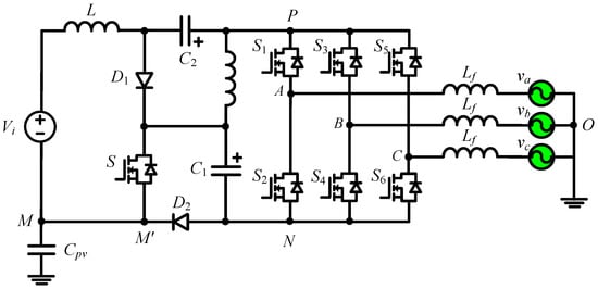
Figure 1.
Three-phase active quasi-Z-source inverter (AqZSI).
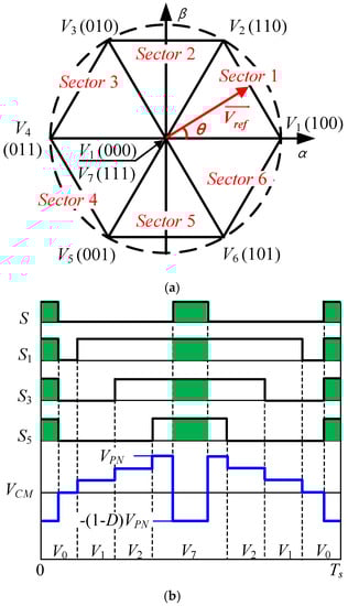
Figure 2.
Three-phase AqZSI using conventional SVM method. (a) SVM diagram; (b) switching pattern in Sector 1.

Table 1.
CMV values for all vectors of AqZSI using conventional SVM method.
3. Modified Active Quasi-Z-Source Topology with Proposed CMV-SVM Method
3.1. Operating Principle of MAqZS Topology
Figure 3 depicts the reconfiguration of MAqZSI. In this case, a DC power supply was connected to two inductors at the positive and negative nodes. Note that the values of inductors L1 and L2 were assumed to be related by L1 = k × L2 (k is the inductance ratio). Similar to the conventional Z-source inverter, the MAqZSI also has shoot-through and non-shoot-through modes, as shown in Figure 4b. For the shoot-through mode, the following equations may be derived:
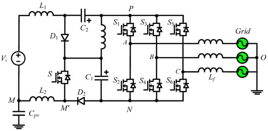
Figure 3.
Three-phase modified active quasi-Z-source inverter (MAqZSI).
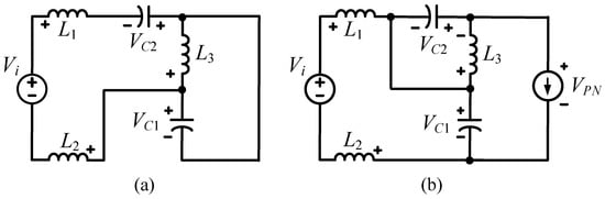
Figure 4.
Equivalent circuit of MAqZSI. (a) Shoot-through mode, (b) Non-shoot-through mode.
For the non-shoot-through mode, the following equations may be derived:
Applying the volt-second balance for inductors L1, L2, and L3, we have
where D is the shoot-through duty cycle.
Thus, the voltage gain of the MAqZSI can be given
3.2. CMV of MAqZSI
The common-mode loop model of the three-phase MAqZSI PV system is shown in Figure 5. The voltage between nodes M and M’ is the inductor L2 voltage. Moreover, the CMV VCM is the total voltage of the VON and VNM. From Figure 5, VCM may be expressed as
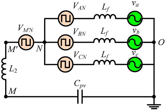
Figure 5.
Common-mode model of three-phase MAqZSI.
According to the operating analysis shown in Figure 4 and Figure 5, the CMV values in the switching states of MAqZSI were calculated in Table 2. When the MAqZSI was operated in the non-shoot-through mode, it meant that the inverter operated with odd and event vectors. Thus, the CMV of MAqZSI can be derived as
where k = L1/L2 and k > 0.
Table 2.
CMV values for MAqZSI with proposed CMV-SVM reduction method.
From Equation (6), the peak-to-peak voltage of CMV is VPN/3 for all values of k. However, when the shoot-through states are inserted, another level of CMV occurs in each shoot-through state. Furthermore, the peak-to-peak CMV can be increased. The CMV of MAqZSI with odd, even, and shoot-through vectors can be obtained as
From (7), we can show that the variation value of CMV was minimized and equal to VPN/3 by changing the value of k. Thus, the CMV variation could be maintained at VPN/3 and the value of k should be 1/(5 − 3D) ≤ k ≤ 2/(4 − 3D). In this case, the value of k = 1/4 was chosen. The peak-to-peak CMV of the MAqZSI with the proposed SVM is approximately one-sixth of the peak-to-peak CMV of the AqZSI using the conventional SVM control.
3.3. Implementation of the Proposed CMR-SVM Method
The proposed CMV-SVM reduction method for MAqZSI is based on the near-state SVM method, as shown in Figure 6. In this case, MAqZSI was operated without shoot-through states. The vector , , and time intervals were defined as Ta, Tb, and T0, respectively. The MAqZSI reference voltage vector was derived as
where Ts is the control cycle.

Figure 6.
Space vector diagram of the proposed CMR-SVM method without shoot-through states. (a) SVM diagram and (b) switching states in Sector 1.
The values of Ta, Tb, and T can be defined as
where δ is the inclined angle, Mi is the modulation index and equals to
where Vref is the output phase voltage.
In the proposed CMV-SVM reduction method for MA-qZSI, Sector 1 is taken as an example, as shown in Figure 6b. In this case, the proposed CMV-SVM executes with the sequence V2–V1–V6–V1–V2 with a commutation step of 60°. It can be seen that the proposed CMV-SVM reduction method for the MAqZSI in the non-ST state was operated as the conventional NS-SVM method, and one vector was used to replace . Furthermore, the time interval of was defined as T6 = Tz. Then, the variation of the CMV was reduced to one-third of the DC-link voltage.
When the boost capability is required, the shoot-through states must be inserted into the switching sequences of the proposed CMV-SVM reduction method for MAqZSI. In this case, the proposed CMV-SVM reduction method for MAqZSI was executed with one more shoot-through vector. The space vector diagram of the proposed CMV-SVM reduction method for MA-qZSI with the shoot-through state insertion is shown in Figure 7a. According to the space vector diagram, the ST states can be inserted into vector . The switching sequences in the next sectors of the proposed CMV-SVM reduction method for MA-qZSI can also be obtained following this insertion. Similar to the CMV in the non-shoot-through mode, the variation of CMV with shoot-through insertions was also reduced to one-third of the DC-link voltage, as shown in Figure 7b. The MAqZSI reference voltage vector was rewritten as
where and T0 are the shoot-through voltage vectors and the time interval of .
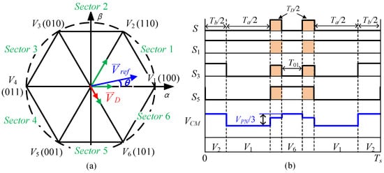
Figure 7.
Space vector diagram of the proposed CMR-SVM method with shoot-through states insertion. (a) SVM diagram and (b) switching states in Sector 1.
The times of , , and were rewritten as
where TD is the interval time of the shoot-through states and equal to D × T.
The modulation index and the shoot-through duty cycle are derived
4. Passive Component Selection
4.1. Inductance Selection
To select the inductance of inductors L1, L2, and L3, only the high-frequency ripple of these inductors is considered. According to Figure 6, the peak-to-peak ripple inductor current with the proposed CMR-SVM method shoot-through state insertion was the highest. From Equation (3), we obtain the following equation:
Based on Equations (2) and (3), the inductance values of L1, L2, and L3 in the proposed CMV-SVM reduction method for MA-qZSI were derived
where ΔIL1 and ΔIL3 are the current ripples of inductors L1 and L3, respectively.
4.2. Capacitance Selection
Similar to the inductor selection, to choose the capacitance of capacitors C1 and C2, the selection only considered the high-frequency ripple. The proposed CMV-SVM reduction method for MAqZSI also produced the highest peak-to-peak voltage ripple under the ST state. From Equations (2)–(4), the capacitance of the C1 and C2 capacitors of MAqZSI were derived as
where ΔVC1 and ΔVC2 are the voltage ripples of capacitors C1 and C2, respectively. IPN is the average DC-link current and is defined as:
4.3. Comparison with Other Two-Level Three-Phase Z-Source Inverters
Table 3 presents the comparison between other Z-source inverter with CMV reduction and the MAqZSI with the proposed SVM method. Regarding the component count, the proposed inverter uses more components in the impedance-source network when compared with the ZS/qZS topologies in [26,27,28,29]. When compared with the modified qSBI [29], the proposed inverter uses one less switch and has lower voltage stress on components, as presented in [18,19]. As shown in Table 3, the ZSI [26] and qZSI [28] can offer the constant CMV. However, the modulation index of these inverters is low. This leads to reduce the output voltage quality and increase the voltage stress on components. The CMV of the modified ZSI [27] and qSBI [29] is equal one-third of the DC-link voltage. Moreover, these inverters can operate in high modulation index. As shown in Figure 8, the proposed inverter has the highest voltage boosting capability. Thus, the proposed inverter can use higher modulation index to improve the output voltage quality.
Table 3.
Comparison between the MAqZSI with other CMV reduction Z-source inverters.
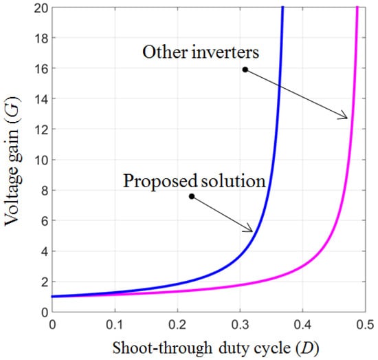
Figure 8.
Voltage gain comparison.
5. Results
5.1. Simulation Results
To validate the effectiveness of the MAqZSI with the proposed CMV-SVM reduction method, a PSIM simulation verification was performed. The system parameters used for the simulation are listed in Table 4. The value of k = 1/4 was used for the ratio of inductances L1 and L2, and the inductance values of L1, L2, and L3 were selected as 1 mH and 4 mH, and 2 mH, respectively. The two capacitors C1 and C2 were 680 µF/450 V and 680 µF/100 V, respectively. The switching frequency was 10 kHz. On the output side, an output filter of 1 mH and 20 μF was used.
Table 4.
Parameters of the MAqZSI.
Figure 9 shows the simulation and experimental results of the output current, output voltage before the output filter, DC-link voltage, and CMV of the AqZSI using the conventional SVM. An input voltage of 250 V and a shoot-through duty cycle of 0.11 was applied to produce a 363 V DC-link voltage. In this case, the modulation index was selected as 0.78 to generate a 110 Vrms output phase voltage. The power load was 1 kW. The peak-to-peak voltage of CMV in the AqZSI using the conventional SVM method was 686 V, as depicted in Figure 9e.


Figure 9.
AqZSI under the conventional SVM method. (a,c,e) Simulation results and (b,d,f) experimental results. From top to bottom: input voltage, output currents, capacitor C1 voltage, vab voltage, DC-link voltage, and CMV.
In the case of the MAqZSI with the proposed CMV-SVM reduction method, the testing parameters were the same as those of the AqZSI using the conventional SVM method. Figure 10 shows the simulation results of the MAqZSI with the proposed CMV-SVM reduction method when an inverter is operated with Vi = 350 V and D = 0. The DC-link voltage is equal to the input voltage and the peak-to-peak voltage is 117 V, as shown in Figure 10e. Moreover, the simulation and experimental results of the MAqZSI with the proposed CMV-SVM reduction method are depicted in Figure 11 when an inverter is operated with Vi = 250 V and D = 0.11. In this case, the DC-link voltage is 363 V and the peak-to-peak voltage of the CMV in the MAqZSI with the proposed CMV-SVM reduction method is 121 V, as shown in Figure 11e. Moreover, to reduce the input voltage of 100 V, the shoot-through duty cycle of 0.28 is applied. In this case, the DC-link voltage is 405 V and the peak-to-peak voltage of the CMV is 135 V, as shown in Figure 12e. It can be seen that the peak-to-peak voltage of the CMV is always equal to one-third of the DC-link voltage in simulations.


Figure 10.
MAqZSI under the proposed CMV-SVM reduction method when Vi = 350 V, D = 0. (a,c,e) Simulation results and (b,d,f) experimental results. From top to bottom: input voltage, output currents, capacitor C1 voltage, vab voltage, DC-link voltage, and CMV.
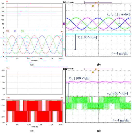

Figure 11.
MAqZSI under the proposed CMV-SVM reduction method when Vi = 250 V, D = 0.11. (a,c,e) Simulation results and (b,d,f) experimental results. From top to bottom: input voltage, output currents, capacitor C1 voltage, vab voltage, DC-link voltage, and CMV.


Figure 12.
MAqZSI under the proposed CMV-SVM reduction method when Vi = 100 V, D = 0.28. (a,c,e) Simulation results and (b,d,f) Experimental results. From top to bottom: input voltage, output currents, capacitor C1 voltage, vab voltage, DC-link voltage, and CMV.
5.2. Experimental Results
To verify the characteristics of the proposed CMV-SVM reduction method for the MAqZSI, a 1 KW three-phase test for AqZSI and MAqZSI was executed. Both the experimental test of AqZSI under the conventional SVM method and MAqZSI with the proposed CMV-SVM reduction method were set up in the same manner as in the simulation. The CMV of the AqZSI with the conventional SVM method changed from −315 V to 350 V as shown in Figure 9f, which was approximately double the DC-link voltage and equal 665 V.
Figure 10b, Figure 11b, and Figure 12b depict that the output currents were 3.5 Arms with an input voltage of 350 V, 250 V, and 100 V. As shown in Figure 10d, Figure 11d, and Figure 12d, the voltage across capacitor C1 was 345 V, 315 V, and 290 V. From Figure 10f, Figure 11f, and Figure 12f, the DC-link voltage for each case was 345 V, 360 V, and 390 V. The peak-to-peak voltage of the CMV is 115 V, 120 V, and 130 V. In the case of MAqZSI with the proposed CMV-SVM reduction method, the CMV voltage was one-third of the DC-link voltage in experiment, which was also approximately 16.67% of the peak-to-peak CMV in the case of AqZSI with the conventional SVM method. A good correlation can be seen between the simulation and experimental verifications.
6. Conclusions
In this article, the SVM method has been proposed for a three-phase MAqZSI topology to decrease the CMV. The MAqZSI with the proposed CMR-SVM method can reduce the instantaneous peak-to-peak voltage of the CMV to one-third of the DC-link voltage. In the MAqZSI, the CMV using the proposed CMR-SVM method was approximately equal to one-sixth of the CMV in AqZSI using the conventional SVM method. Then, the implementation of the MAqZSI with the proposed CMR-SVM method was executed with a 1 kW three-phase inverter prototype. The theoretical operating principles were verified using simulation and experimental results.
Author Contributions
This article has received the same contributions from the authors, which include writing the paper and experiment implementation. This manuscript has received agreement from all authors. All authors have read and agreed to the published version of the manuscript.
Funding
This study was supported by a research fund by the National Research Foundation of Korea (NRF) grant funded by the Korean government (MSIT) NRF-2019R1F1A1059763.
Data Availability Statement
Data are contained within the article.
Acknowledgments
This work was supported by the National Research Foundation of Korea (NRF) grant funded by the Korean government (MSIT) (No. NRF-2019R1F1A1059763). This work was supported by the Gwangju.Jeonnam local Energy Cluster Manpower training of the Korea Institute of Energy Technology Evaluation and Planning (KETEP) grant funded by the Korean government Ministry of Knowledge Economy (No. 20214000000560).
Conflicts of Interest
The authors declare no conflict of interest.
References
- Zhang, L.; Sun, K.; Feng, L.-L.; Wu, H.-F.; Xing, Y. A family of neutral point clamped full-bridge topologies for transformerless photovoltaic grid-tied inverters. IEEE Trans. Power Electron. 2013, 28, 730–739. [Google Scholar] [CrossRef]
- Kouro, S.; Leon, J.-I.; Vinnikov, D.; Franquelo, L.G. Grid-connected photovoltaic systems: An overview of recent research and emerging PV converter technology. IEEE Ind. Electron. Mag. 2015, 9, 47–61. [Google Scholar] [CrossRef]
- Meneses, D.; Blaabjerg, F.; Garcıa, O.; Cobos, J.A. Review and comparison of step-up transformerless topologies for photovoltaic ac-module application. IEEE Trans. Power Electron. 2013, 28, 2649–2663. [Google Scholar] [CrossRef] [Green Version]
- Lopez, O.; Freijedo, F.-D.; Yepes, A.-G.; Fernandez, P.-C.; Malvar, J.; Teodorescu, R.; Doval, J. –G. Eliminating ground current in a transformerless photovoltaic application. IEEE Trans. Energy Convers. 2010, 25, 140–147. [Google Scholar] [CrossRef]
- Guo, X.; Zhang, X.; Guan, H.; Kerekes, T.; Blaabjerg, F. Three-phase ZVR topology and modulation strategy for transformerless PV system. IEEE Trans. Power Electron. 2019, 34, 1017–1021. [Google Scholar] [CrossRef] [Green Version]
- Guo, X.; He, R.; Jian, J.; Lu, Z.; Sun, X.; Guerrero, J.-M. Leakage current elimination of four-leg inverter for transformerless three-phase PV systems. IEEE Trans. Power Electron. 2016, 31, 1841–1846. [Google Scholar] [CrossRef] [Green Version]
- Gupta, A.-K.; Agrawal, H.; Agarwal, V. A Novel three-phase transformerless H-8 topology with reduced leakage current for grid-tied solar PV applications. IEEE Trans. Ind. Appl. 2019, 55, 1765–1774. [Google Scholar] [CrossRef]
- Anand, S.; Gundlapalli, S.K.; Fernandes, B.-G. Transformer-less grid feeding current source inverter for solar photovoltaic system. IEEE Trans. Ind. Electron. 2014, 61, 5334–5344. [Google Scholar] [CrossRef]
- Tran, T.T.; Nguyen, M.K.; Duong, T.D.; Choi, J.H.; Lim, Y.C.; Zare, F. A Switched-Capacitor-Voltage-Doubler Based Boost Inverter for Common-Mode Voltage Reduction. IEEE Access 2019, 7, 98618–98629. [Google Scholar] [CrossRef]
- Hou, C.; Shih, C.; Cheng, P.; Hava, A.-M. Common-mode voltage reduction pulse-width modulation techniques for three-phase grid-connected converters. IEEE Trans. Power Electron. 2013, 28, 1971–1979. [Google Scholar] [CrossRef]
- Chen, H.; Zhao, H. Review on pulse-width modulation strategies for common-mode voltage reduction in three-phase voltage-source inverters. IET Power Electron. 2016, 9, 2611–2620. [Google Scholar] [CrossRef]
- Janabi, A.; Wang, B. Hybrid SVPWM scheme to minimize the common-mode voltage frequency and amplitude in voltage source inverter drives. IEEE Trans. Power Electron. 2019, 34, 1595–1610. [Google Scholar] [CrossRef]
- Liu, Y.; Ge, B.; Abu, R.-H.; Sun, D. Comprehensive modeling of single-phase quasi-Z-source photovoltaic inverter to investigate low frequency voltage and current ripple. IEEE Trans. Ind. Electron. 2015, 62, 4194–4202. [Google Scholar] [CrossRef]
- Rahman, M.-M.; Iqbal, A.; Ben-Brahim, L.; Abu-Rub, H.; Khan, I. Novel Level-Shifted PWM Technique for Cascaded Multilevel Quasi-Impedance Source Inverter. IEEE J. Emerg. Sel. Top. Power Electron. 2021, 9, 5918–5928. [Google Scholar] [CrossRef]
- Barath, J.N.; Soundarrajan, A.; Stepenko, S.; Husev, O.; Vinnikov, D.; Nguyen, M.-K. Topological Review of Quasi-Switched Boost Inverters. Electronics 2021, 10, 1485. [Google Scholar] [CrossRef]
- Nguyen, M.-K.; Duong, T.-D.; Lim, Y.-C.; Choi, J.-H.; Vilathgamuwa, D.-M.; Walker, G.-R. DC-Link quasi-switched boost inverter with improved PWM strategy and its comparative evaluation. IEEE Access 2020, 8, 53857–53867. [Google Scholar] [CrossRef]
- Nguyen, M.-K.; Choi, Y.-O. Maximum boost control method for single-phase quasi-switched-boost and quasi-Z-source inverters. Energies 2017, 10, 553. [Google Scholar] [CrossRef]
- Nguyen, M.-K.; Duong, T.-D.; Lim, Y.-C.; Choi, J.-H. High Voltage Gain Quasi-Switched Boost Inverters with Low Input Current Ripple. IEEE Trans. Ind. Inform. 2018, 15, 4857–4866. [Google Scholar] [CrossRef]
- Duong, T.-D.; Nguyen, M.-K.; Lim, Y.-C.; Choi, J.-H.; Vilathgamuwa, D.-M. SiC-Based Active Quasi-Z-Source Inverter with Improved PWM Control Strategy. IET Power Electron. 2019, 12, 3810–3821. [Google Scholar] [CrossRef]
- Qin, C.; Zhang, C.; Chen, A.; Xing, X.; Zhang, G. A space vector modulation scheme of the quasi-Z-source three-level T-type inverter for common-mode voltage reduction. IEEE Trans. Ind. Electron. 2018, 65, 8340–8350. [Google Scholar] [CrossRef]
- Li, X.; Xing, X.; Zhang, C.; Chen, A.; Qin, C.; Zhang, G. Simultaneous common-mode resonance circulating current and leakage current suppression for transformerless three-level T-type PV inverter system. IEEE Trans. Ind. Electron. 2019, 66, 4457–4467. [Google Scholar] [CrossRef]
- Nicolas, M.; Carlos, R.-C.; Ana, M.-L.; Oleksandr, H. A simple space vector modulation method with DC-link voltage balancing and reduced common-mode voltage strategy for a three-level T-type quasi-Z source inverter. IEEE Access 2021, 9, 82747–82760. [Google Scholar]
- Guo, X.; Yang, Y.; He, R.; Wang, B.; Blaabjerg, F. Leakage current reduction of three-phase Z-source three-level four-leg inverter for transformerless PV system. IEEE Trans. Power Electron. 2019, 34, 6299–6308. [Google Scholar] [CrossRef]
- Guo, X.; Yang, Y.; He, R.; Wang, B.; Blaabjergm, F. Transformerless Z-source four-leg PV inverter with leakage current reduction. IEEE Trans. Power Electron. 2019, 34, 4343–4352. [Google Scholar] [CrossRef]
- Noroozi, N.; Yaghoubi, M.; Zolghadri, M.R. A modulation method for leakage current reduction in a three-phase grid-tie quasi-Z-source inverter. IEEE Trans. Power Electron. 2019, 34, 5439–5450. [Google Scholar] [CrossRef]
- Bradaschia, F.; Cavalcanti, M.-C.; Ferraz, P.-E.-P.; Neves, F.-A.-S. Modulation for three-phase transformerless Z-source inverter to reduce leakage currents in photovoltaic systems. IEEE Trans. Ind. Electron. 2011, 58, 5385–5395. [Google Scholar] [CrossRef]
- Erginer, V.; Sarul, M.H. A novel reduced leakage current modulation technique for Z-source inverter used in photovoltaic systems. IET Power Electron. 2014, 7, 496–502. [Google Scholar] [CrossRef]
- Noroozi, N.; Zolghadri, M.-R. Three-phase quasi-Z-source inverter with constant common-mode voltage for photovoltaic application. IEEE Trans. Ind. Electron. 2018, 65, 4790–4798. [Google Scholar] [CrossRef]
- Duong, T.-D.; Nguyen, M.-K.; Tran, T.-T.; Lim, Y.-C.; Choi, J.-H.; Wang, C. Modulation Techniques for a Modified Three-Phase Quasi-Switched Boost Inverter with Common-Mode Voltage Reduction. IEEE Access 2020, 8, 160670–160683. [Google Scholar] [CrossRef]
Publisher’s Note: MDPI stays neutral with regard to jurisdictional claims in published maps and institutional affiliations. |
© 2021 by the authors. Licensee MDPI, Basel, Switzerland. This article is an open access article distributed under the terms and conditions of the Creative Commons Attribution (CC BY) license (https://creativecommons.org/licenses/by/4.0/).