
A Noise-Resilient Neuromorphic Digit Classifier Based on NOR Flash Memories with Pulse–Width Modulation Scheme


Abstract
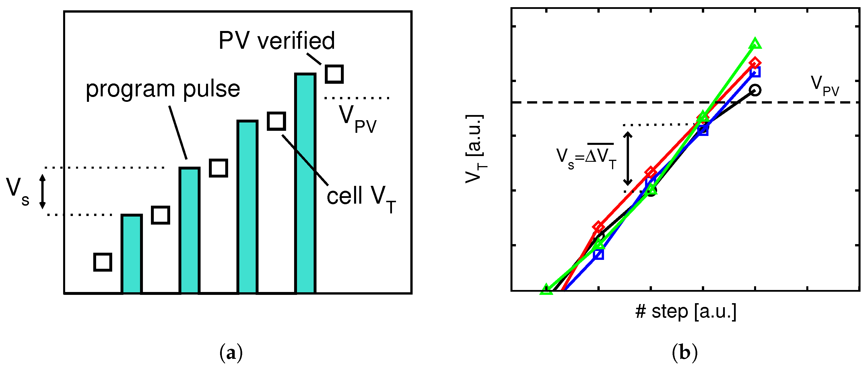
:1. Introduction
2. Noise-Sensitivity Reduction Techniques in ANNs
3. Pulse Amplitude Modulation
4. Pulse Width Modulation
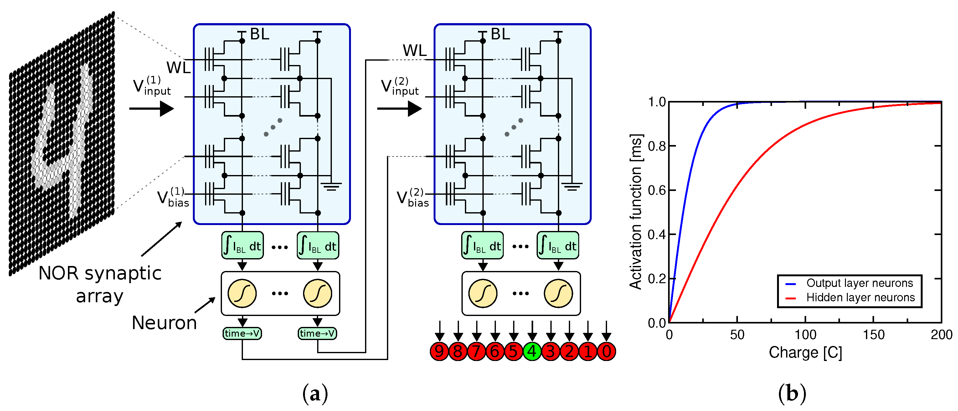
5. Neuromorphic Digit Classifier Based on PWM
6. Noise-Sensitivity Analysis of the Classifier Performance
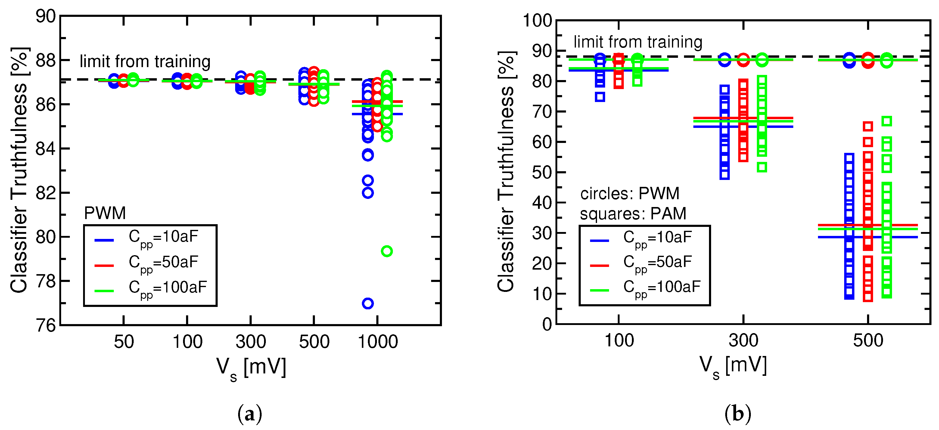
6.1. Impact of Program Noise
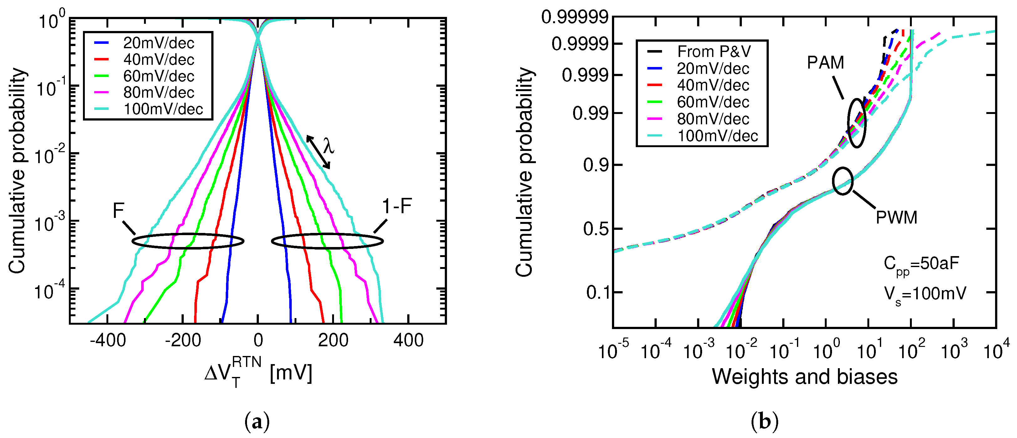
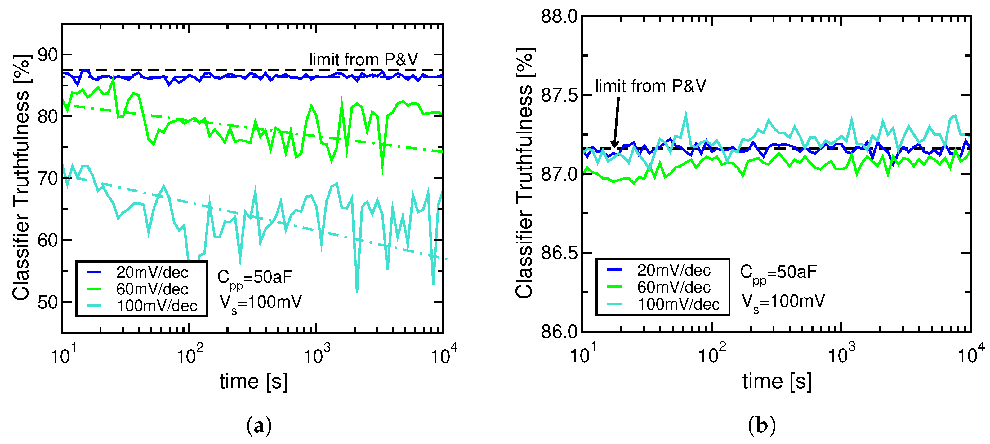
6.2. Impact of RTN
6.3. Impact of Temperature Variations
7. Conclusions
Author Contributions
Funding
Acknowledgments
Conflicts of Interest
References
- Burr, G.W.; Shelby, R.M.; Sebastian, A.; Kim, S.; Kim, S.; Sidler, S.; Virwani, K.; Ishii, M.; Narayanan, P.; Fumarola, A.; et al. Neuromorphic computing using non-volatile memory. Adv. Phys. X 2017, 2, 89–124. [Google Scholar] [CrossRef]
- Merrikh-Bayat, F.; Guo, X.; Klachko, M.; Prezioso, M.; Likharev, K.K.; Strukov, D.B. High-performance mixed-signal neurocomputing with nanoscale floating-gate memory cell arrays. IEEE Trans. Neural Netw. Learn. Syst. 2017, 29, 4782–4790. [Google Scholar] [CrossRef] [PubMed]
- Ielmini, D. Resistive switching memories based on metal oxides: Mechanisms, reliability and scaling. Semicond. Sci. Technol. 2016, 31, 063002. [Google Scholar] [CrossRef]
- Prezioso, M.; Merrikh-Bayat, F.; Hoskins, B.; Adam, G.C.; Likharev, K.K.; Strukov, D.B. Training and operation of an integrated neuromorphic network based on metal-oxide memristors. Nature 2015, 521, 61–64. [Google Scholar] [CrossRef] [Green Version]
- Yu, S.; Chen, P.Y.; Cao, Y.; Xia, L.; Wang, Y.; Wu, H. Scaling-up resistive synaptic arrays for neuro-inspired architecture: Challenges and prospect. In Proceedings of the 2015 IEEE International Electron Devices Meeting, Washington, DC, USA, 7–9 December 2015; pp. 451–454. [Google Scholar] [CrossRef]
- Raoux, S.; Wełnic, W.; Ielmini, D. Phase change materials and their application to nonvolatile memories. Chem. Rev. 2010, 110, 240–267. [Google Scholar] [CrossRef] [PubMed]
- Burr, G.W.; Shelby, R.M.; Sidler, S.; Di Nolfo, C.; Jang, J.; Boybat, I.; Shenoy, R.S.; Narayanan, P.; Virwani, K.; Giacometti, E.U.; et al. Experimental demonstration and tolerancing of a large-scale neural network (165,000 synapses) using phase-change memory as the synaptic weight element. IEEE Trans. Electron Devices 2015, 62, 3498–3507. [Google Scholar] [CrossRef]
- Merrikh-Bayat, F.; Guo, X.; Om’Mani, H.; Do, N.; Likharev, K.K.; Strukov, D.B. Redesigning commercial floating-gate memory for analog computing applications. In Proceedings of the 2015 IEEE International Symposium on Circuits and Systems, Lisbon, Portugal, 24–27 May 2015; pp. 1921–1924. [Google Scholar] [CrossRef] [Green Version]
- Guo, X.; Merrikh-Bayat, F.; Bavandpour, M.; Klachko, M.; Mahmoodi, M.; Prezioso, M.; Likharev, K.; Strukov, D. Fast, energy-efficient, robust, and reproducible mixed-signal neuromorphic classifier based on embedded NOR Flash memory technology. In Proceedings of the 2017 IEEE International Electron Devices Meeting, San Francisco, CA, USA, 2–6 December 2017; pp. 151–154. [Google Scholar] [CrossRef]
- Guo, X.; Bayat, F.M.; Prezioso, M.; Chen, Y.; Nguyen, B.; Do, N.; Strukov, D.B. Temperature-insensitive analog vector-by-matrix multiplier based on 55 nm NOR Flash memory cells. In Proceedings of the 2017 IEEE Custom Integrated Circuits Conference, Austin, TX, USA, 30 April–3 May 2017; pp. 1–4. [Google Scholar] [CrossRef] [Green Version]
- Malavena, G.; Sottocornola Spinelli, A.; Monzio Compagnoni, C. Implementing spike-timing-dependent plasticity and unsupervised learning in a mainstream NOR Flash memory array. In Proceedings of the 2018 IEEE International Electron Devices Meeting, San Francisco, CA, USA, 1–5 December 2018; pp. 35–38. [Google Scholar] [CrossRef]
- Malavena, G.; Filippi, M.; Sottocornola Spinelli, A.; Monzio Compagnoni, C. Unsupervised learning by spike-timing-dependent plasticity in a mainstream NOR Flash memory array—Part I: Cell operation. IEEE Trans. Electron Devices 2019, 66, 4727–4732. [Google Scholar] [CrossRef]
- Malavena, G.; Filippi, M.; Sottocornola Spinelli, A.; Monzio Compagnoni, C. Unsupervised learning by spike-timing-dependent plasticity in a mainstream NOR Flash memory array—Part II: Array learning. IEEE Trans. Electron Devices 2019, 66, 4733–4738. [Google Scholar] [CrossRef]
- Lee, S.T.; Lim, S.; Choi, N.; Bae, J.H.; Kim, C.H.; Lee, S.; Lee, D.H.; Lee, T.; Chung, S.; Park, B.G.; et al. Neuromorphic technology based on charge storage memory devices. In Proceedings of the 2018 IEEE Symposium on VLSI Technology, Honolulu, HI, USA, 18–22 June 2018; pp. 169–170. [Google Scholar] [CrossRef]
- Lee, S.T.; Lim, S.; Choi, N.Y.; Bae, J.H.; Kwon, D.; Park, B.G.; Lee, J.H. Operation scheme of multi-layer neural networks using NAND Flash memory as high-density synaptic devices. IEEE J. Electron Devices Soc. 2019, 7, 1085–1093. [Google Scholar] [CrossRef]
- Lee, S.T.; Lee, J.H. Neuromorphic computing using NAND Flash memory architecture with pulse width modulation scheme. Front. Neurosci. 2020, 14, 945. [Google Scholar] [CrossRef]
- Milo, V.; Malavena, G.; Monzio Compagnoni, C.; Ielmini, D. Memristive and CMOS devices for neuromorphic computing. Materials 2020, 13, 166. [Google Scholar] [CrossRef] [Green Version]
- Kim, H.; Park, J.; Kwon, M.W.; Lee, J.H.; Park, B.G. Silicon-based floating-body synaptic transistor with frequency-dependent short-and long-term memories. IEEE Electron Device Lett. 2016, 37, 249–252. [Google Scholar] [CrossRef]
- Kim, H.; Hwang, S.; Park, J.; Yun, S.; Lee, J.H.; Park, B.G. Spiking neural network using synaptic transistors and neuron circuits for pattern recognition with noisy images. IEEE Electron Device Lett. 2018, 39, 630–633. [Google Scholar] [CrossRef]
- Kim, C.H.; Lee, S.; Woo, S.Y.; Kang, W.M.; Lim, S.; Bae, J.H.; Kim, J.; Lee, J.H. Demonstration of unsupervised learning with spike-timing-dependent plasticity using a TFT-type NOR Flash memory array. IEEE Trans. Electron Devices 2018, 65, 1774–1780. [Google Scholar] [CrossRef]
- Nielsen, M.A. Neural Networks and Deep Learning. Determination Press. 2015. Available online: http://neuralnetworksanddeeplearning.com/ (accessed on 12 November 2021).
- Ielmini, D.; Lacaita, A.L.; Mantegazza, D. Recovery and drift dynamics of resistance and threshold voltages in phase-change memories. IEEE Trans. Electron Devices 2007, 54, 308–315. [Google Scholar] [CrossRef]
- Nandakumar, S.; Boybat, I.; Han, J.P.; Ambrogio, S.; Adusumilli, P.; Bruce, R.L.; BrightSky, M.; Rasch, M.; Le Gallo, M.; Sebastian, A. Precision of synaptic weights programmed in phase-change memory devices for deep learning inference. In Proceedings of the 2020 IEEE International Electron Devices Meeting, San Francisco, CA, USA, 12–18 December 2020; pp. 29.4.1–29.4.4. [Google Scholar] [CrossRef]
- Joshi, V.; Le Gallo, M.; Haefeli, S.; Boybat, I.; Nandakumar, S.R.; Piveteau, C.; Dazzi, M.; Rajendran, B.; Sebastian, A.; Eleftheriou, E. Accurate deep neural network inference using computational phase-change memory. Nat. Commun. 2020, 11, 2473. [Google Scholar] [CrossRef]
- Kariyappa, S.; Tsai, H.; Spoon, K.; Ambrogio, S.; Narayanan, P.; Mackin, C.; Chen, A.; Qureshi, M.; Burr, G.W. Noise-Resilient DNN: Tolerating Noise in PCM-Based AI Accelerators via Noise-Aware Training. IEEE Trans. Electron Devices 2021, 68, 4356–4362. [Google Scholar] [CrossRef]
- Long, Y.; She, X.; Mukhopadhyay, S. Design of reliable DNN accelerator with un-reliable ReRAM. In Proceedings of the 2019 IEEE Design, Automation & Test in Europe Conference & Exhibition (DATE), Florence, Italy, 25–29 March 2019; pp. 1769–1774. [Google Scholar] [CrossRef]
- He, Z.; Lin, J.; Ewetz, R.; Yuan, J.S.; Fan, D. Noise injection adaption: End-to-End ReRAM crossbar non-ideal effect adaption for neural network mapping. In Proceedings of the 56th Annual Design Automation Conference 2019, Las Vegas, NV, USA, 2–6 June 2019; pp. 1–6. [Google Scholar] [CrossRef]
- Zheng, Q.; Kang, J.; Wang, Z.; Cai, Y.; Huang, R.; Li, B.; Chen, Y.; Li, H. Enhance the robustness to time dependent variability of ReRAM-based neuromorphic computing systems with regularization and 2R synapse. In Proceedings of the 2019 IEEE International Symposium on Circuits and Systems, Sapporo, Japan, 26–29 May 2019; pp. 1–5. [Google Scholar] [CrossRef]
- Malavena, G.; Petrò, S.; Sottocornola Spinelli, A.; Monzio Compagnoni, C. Impact of program accuracy and random telegraph noise on the performance of a NOR Flash-based neuromorphic classifier. In Proceedings of the IEEE 2019 European Solid-State Device Research Conference, Cracow, Poland, 23–26 September 2019; pp. 122–125. [Google Scholar] [CrossRef]
- Diorio, C.; Hasler, P.; Minch, A.; Mead, C.A. A single-transistor silicon synapse. IEEE Trans. Electron Devices 1996, 43, 1972–1980. [Google Scholar] [CrossRef] [Green Version]
- Diorio, C.; Hasler, P.; Minch, B.A.; Mead, C.A. A floating-gate MOS learning array with locally computed weight updates. IEEE Trans. Electron Devices 1997, 44, 2281–2289. [Google Scholar] [CrossRef] [Green Version]
- Monzio Compagnoni, C.; Sottocornola Spinelli, A.; Gusmeroli, R.; Beltrami, S.; Ghetti, A.; Visconti, A. Ultimate accuracy for the NAND Flash program algorithm due to the electron injection statistics. IEEE Trans. Electron Devices 2008, 55, 2695–2702. [Google Scholar] [CrossRef]
- Boccaccio, C. Embedded 1T Flash NOR: Still alive at 40 nm. And beyond? In Proceedings of the Leti Memory Workshop, Grenoble, France, 25–28 June 2013. [Google Scholar]
- Calligaro, C.; Manstretta, A.; Modelli, A.; Torelli, G. Technological and design constraints for multilevel Flash memories. In Proceedings of the IEEE International Conference on Electronics, Circuits, and Systems, Rhodes, Greece, 16 October 1996; Volume 2, pp. 1005–1008. [Google Scholar] [CrossRef]
- Monzio Compagnoni, C.; Chiavarone, L.; Calabrese, M.; Ghidotti, M.; Lacaita, A.L.; Spinelli, A.S.; Visconti, A. Fundamental limitations to the width of the programmed VT distribution of NOR Flash memories. IEEE Trans. Electron Devices 2010, 57, 1761–1767. [Google Scholar] [CrossRef]
- Goda, A.; Miccoli, C.; Monzio Compagnoni, C. Time dependent threshold-voltage fluctuations in NAND Flash memories: From basic physics to impact on array operation. In Proceedings of the 2015 IEEE International Electron Devices Meeting, Washington, DC, USA, 7–9 December 2015; pp. 374–377. [Google Scholar] [CrossRef]
- Monzio Compagnoni, C.; Gusmeroli, R.; Spinelli, A.S.; Visconti, A. Analytical model for the electron-injection statistics during programming of nanoscale NAND Flash memories. IEEE Trans. Electron Devices 2008, 55, 3192–3199. [Google Scholar] [CrossRef]
- Ghetti, A.; Monzio Compagnoni, C.; Sottocornola Spinelli, A.; Visconti, A. Comprehensive analysis of random telegraph noise instability and its scaling in deca–nanometer Flash memories. IEEE Trans. Electron Devices 2009, 56, 1746–1752. [Google Scholar] [CrossRef]
- Sottocornola Spinelli, A.; Monzio Compagnoni, C.; Gusmeroli, R.; Ghidotti, M.; Visconti, A. Investigation of the random telegraph noise instability in scaled Flash memory arrays. Jpn. J. Appl. Phys. 2008, 47, 2598. [Google Scholar] [CrossRef]
- Adamu-Lema, F.; Monzio Compagnoni, C.; Amoroso, S.M.; Castellani, N.; Gerrer, L.; Markov, S.; Spinelli, A.S.; Lacaita, A.L.; Asenov, A. Accuracy and issues of the spectroscopic analysis of RTN traps in nanoscale MOSFETs. IEEE Trans. Electron Devices 2012, 60, 833–839. [Google Scholar] [CrossRef]
- LeCun, Y.; Bottou, L.; Bengio, Y.; Haffner, P. Gradient-based learning applied to document recognition. Proc. IEEE 1998, 86, 2278–2324. [Google Scholar] [CrossRef] [Green Version]
- Monzio Compagnoni, C.; Gusmeroli, R.; Spinelli, A.S.; Lacaita, A.L.; Bonanomi, M.; Visconti, A. Statistical model for random telegraph noise in Flash memories. IEEE Trans. Electron Devices 2007, 55, 388–395. [Google Scholar] [CrossRef]
- Ghetti, A.; Amoroso, S.M.; Mauri, A.; Monzio Compagnoni, C. Impact of nonuniform doping on random telegraph noise in Flash memory devices. IEEE Trans. Electron Devices 2011, 59, 309–315. [Google Scholar] [CrossRef]
- Amoroso, S.M.; Monzio Compagnoni, C.; Ghetti, A.; Gerrer, L.; Sottocornola Spinelli, A.S.; Lacaita, A.L.; Asenov, A. Investigation of the RTN distribution of nanoscale MOS devices from subthreshold to on-state. IEEE Electron Device Lett. 2013, 34, 683–685. [Google Scholar] [CrossRef] [Green Version]
- Miccoli, C.; Paolucci, G.M.; Monzio Compagnoni, C.; Sottocornola Spinelli, A.S.; Goda, A. Cycling pattern and read/bake conditions dependence of random telegraph noise in decananometer NAND Flash arrays. In Proceedings of the 2015 IEEE International Reliability Physics Symposium, Monterey, CA, USA, 19–23 April 2015; pp. MY.9.1–MY.9.6. [Google Scholar] [CrossRef]


| Input | Output | PN Sensitivity | RTN Sensitivity | Temperature Sensitivity | Energy Efficiency | |
|---|---|---|---|---|---|---|
| PAM | strong | strong | strong | high | ||
| PWM | weak | weak | weak | moderate |
Publisher’s Note: MDPI stays neutral with regard to jurisdictional claims in published maps and institutional affiliations. |
© 2021 by the authors. Licensee MDPI, Basel, Switzerland. This article is an open access article distributed under the terms and conditions of the Creative Commons Attribution (CC BY) license (https://creativecommons.org/licenses/by/4.0/).
Share and Cite
Malavena, G.; Sottocornola Spinelli, A.; Monzio Compagnoni, C. A Noise-Resilient Neuromorphic Digit Classifier Based on NOR Flash Memories with Pulse–Width Modulation Scheme. Electronics 2021, 10, 2784. https://doi.org/10.3390/electronics10222784
Malavena G, Sottocornola Spinelli A, Monzio Compagnoni C. A Noise-Resilient Neuromorphic Digit Classifier Based on NOR Flash Memories with Pulse–Width Modulation Scheme. Electronics. 2021; 10(22):2784. https://doi.org/10.3390/electronics10222784
Chicago/Turabian StyleMalavena, Gerardo, Alessandro Sottocornola Spinelli, and Christian Monzio Compagnoni. 2021. "A Noise-Resilient Neuromorphic Digit Classifier Based on NOR Flash Memories with Pulse–Width Modulation Scheme" Electronics 10, no. 22: 2784. https://doi.org/10.3390/electronics10222784
APA StyleMalavena, G., Sottocornola Spinelli, A., & Monzio Compagnoni, C. (2021). A Noise-Resilient Neuromorphic Digit Classifier Based on NOR Flash Memories with Pulse–Width Modulation Scheme. Electronics, 10(22), 2784. https://doi.org/10.3390/electronics10222784