
Recent Progress on 3D NAND Flash Technologies

Abstract
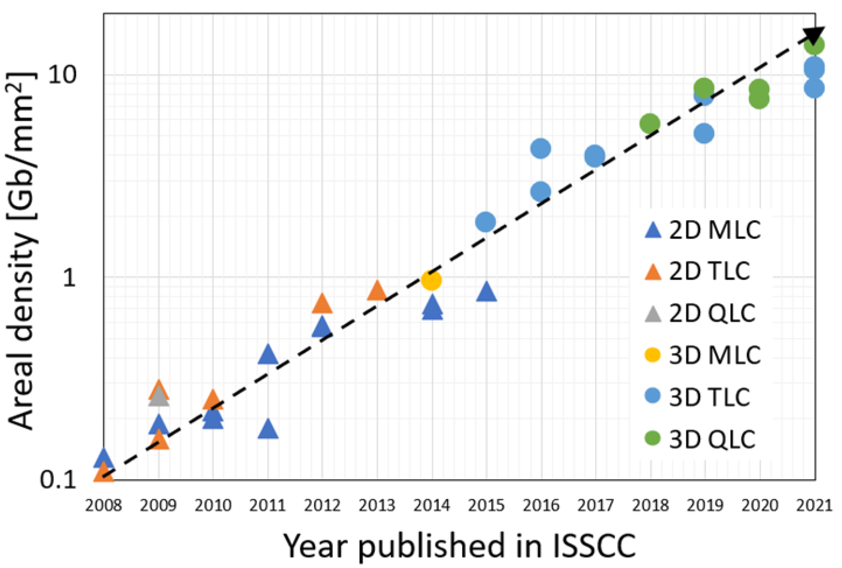
:1. Introduction
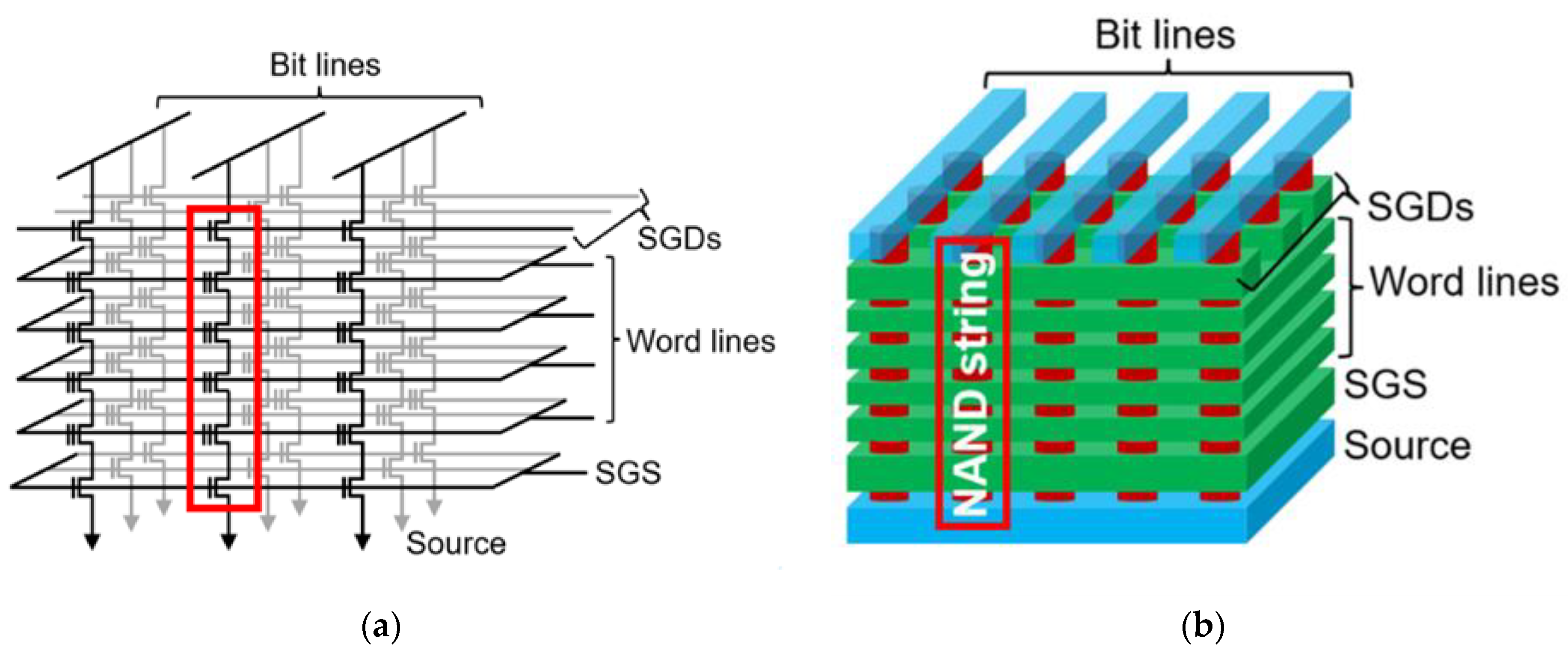
2. 3D NAND Architecture and Operations
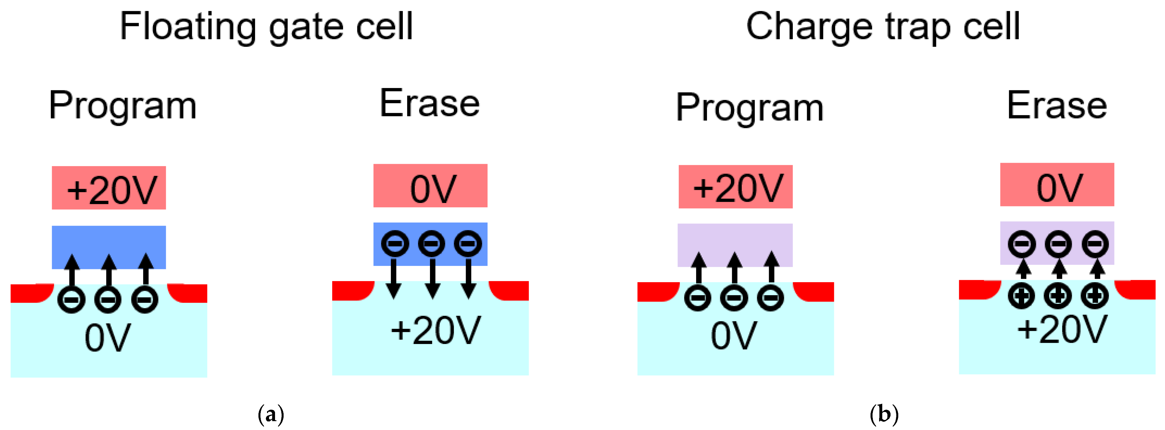
3. Floating Gate NAND and Replacement Gate NAND
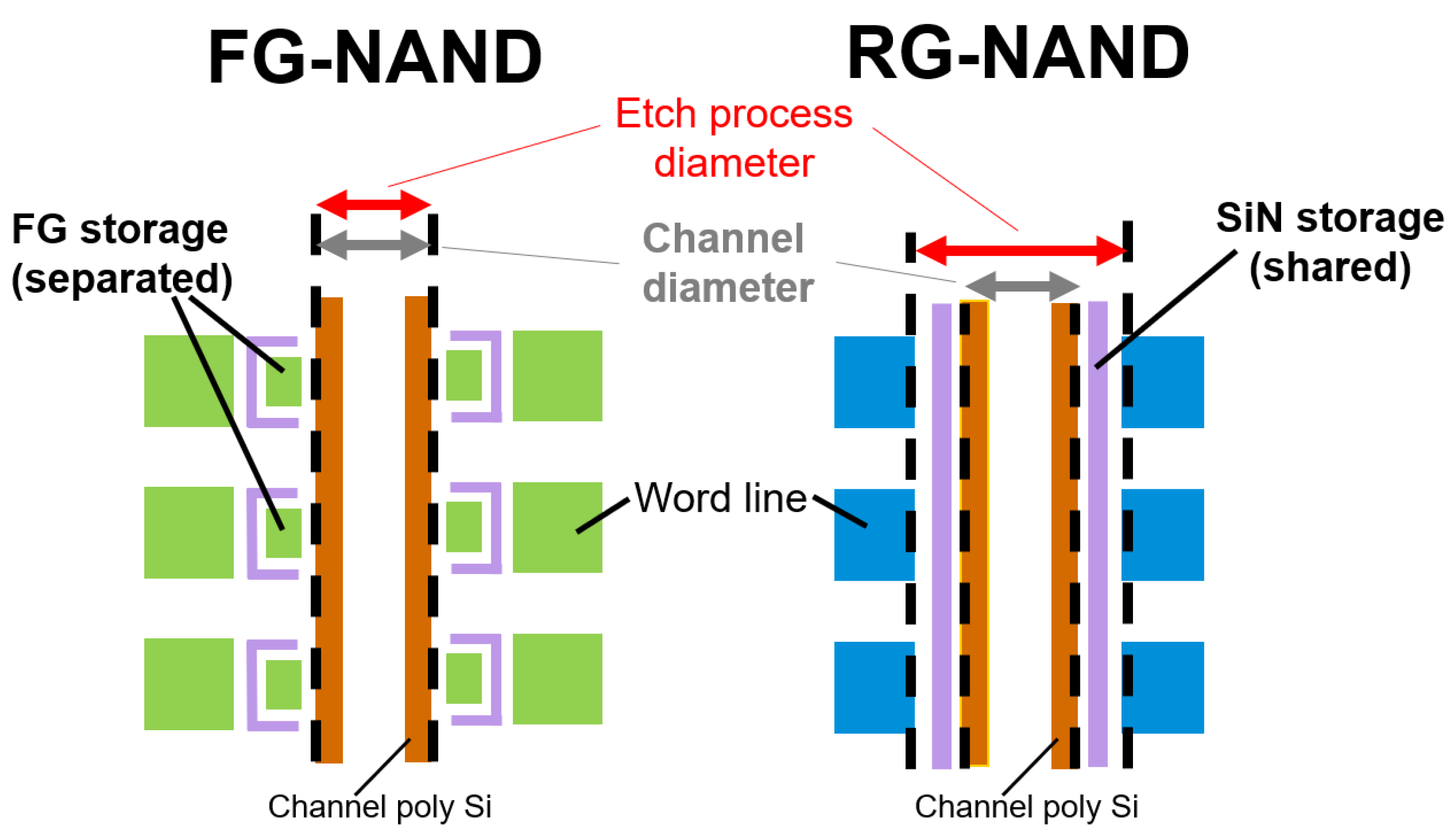
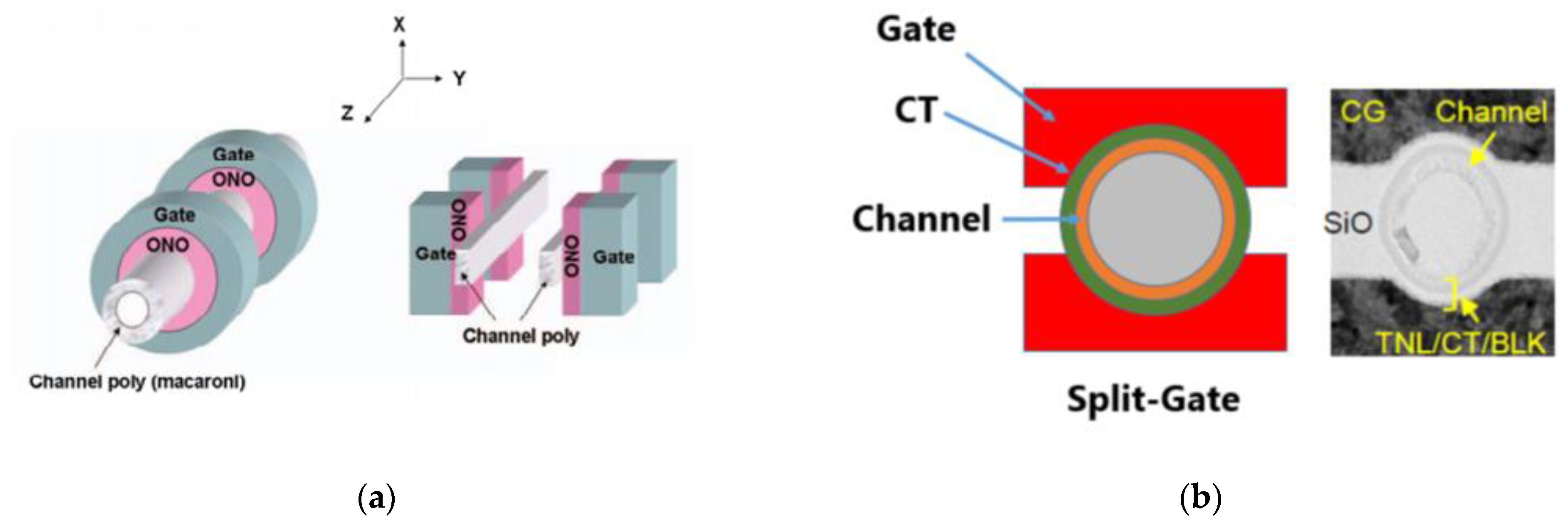
3.1. Architectures of FG NAND and RG NAND
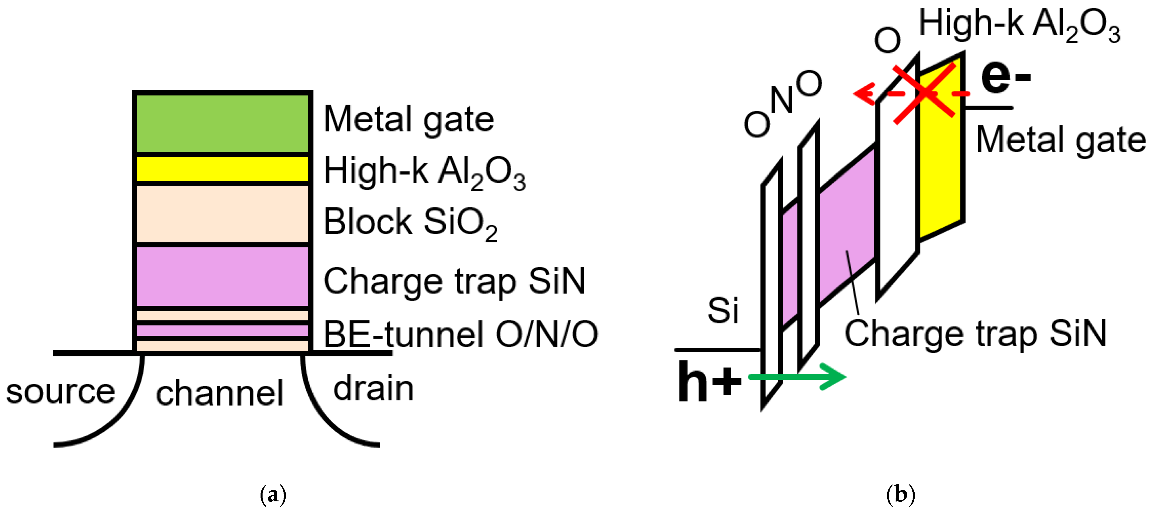
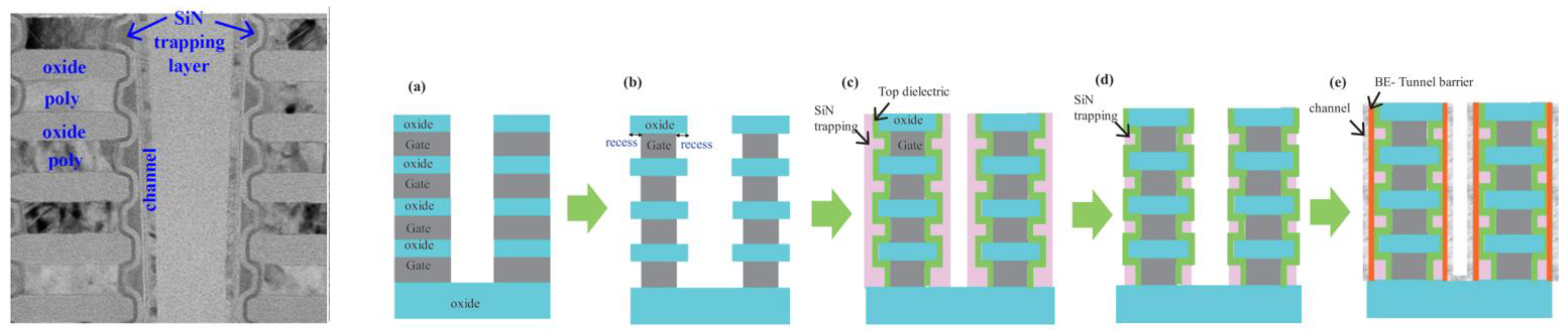
3.2. Band-Engineered Tunneling Dielectrics of the Charge-Trap Cell
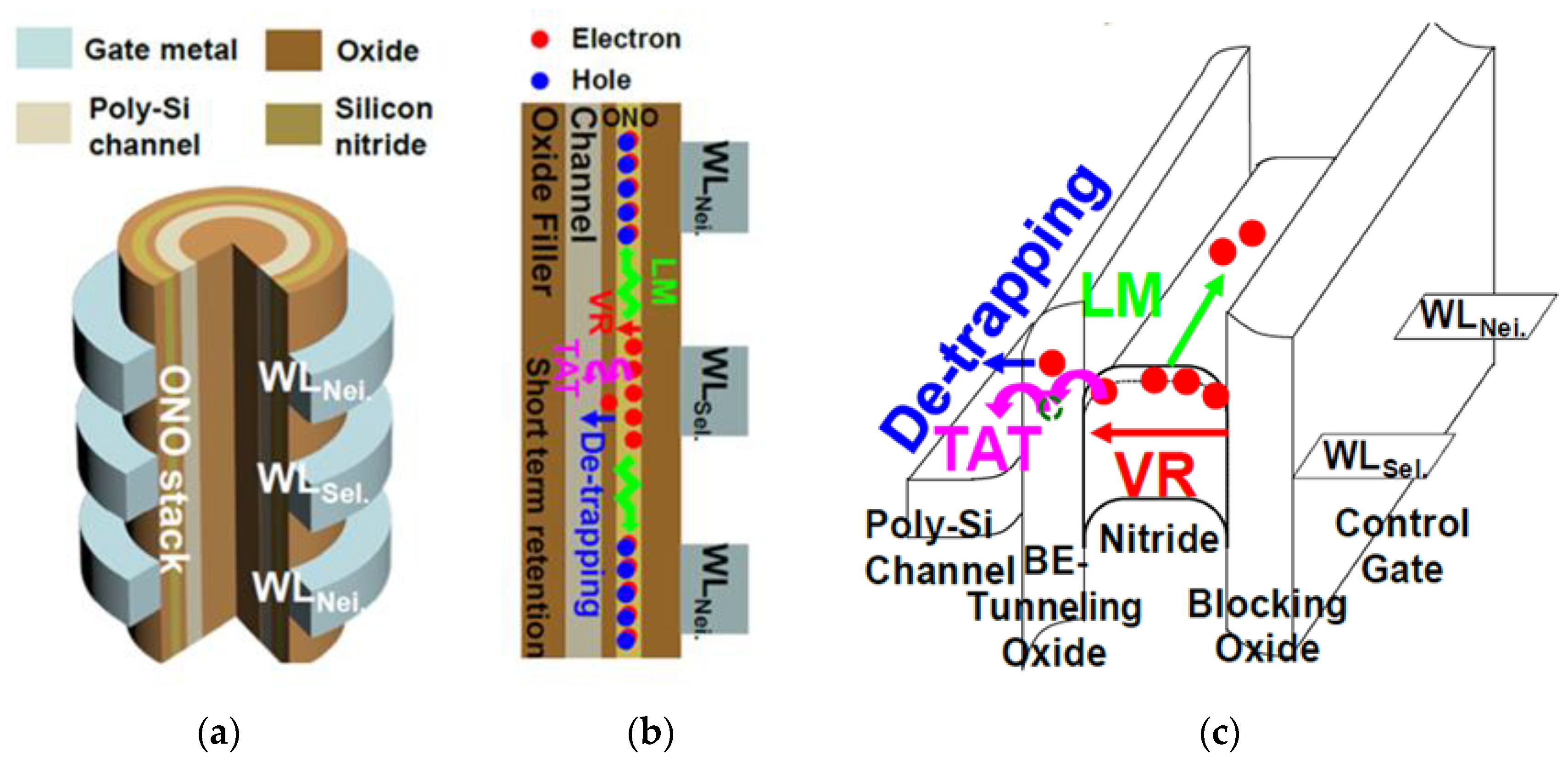
3.3. Data Retention Mechanisms of the Charge-Trap Cell
4. 3D NAND Array Physical Scaling by Process Integration
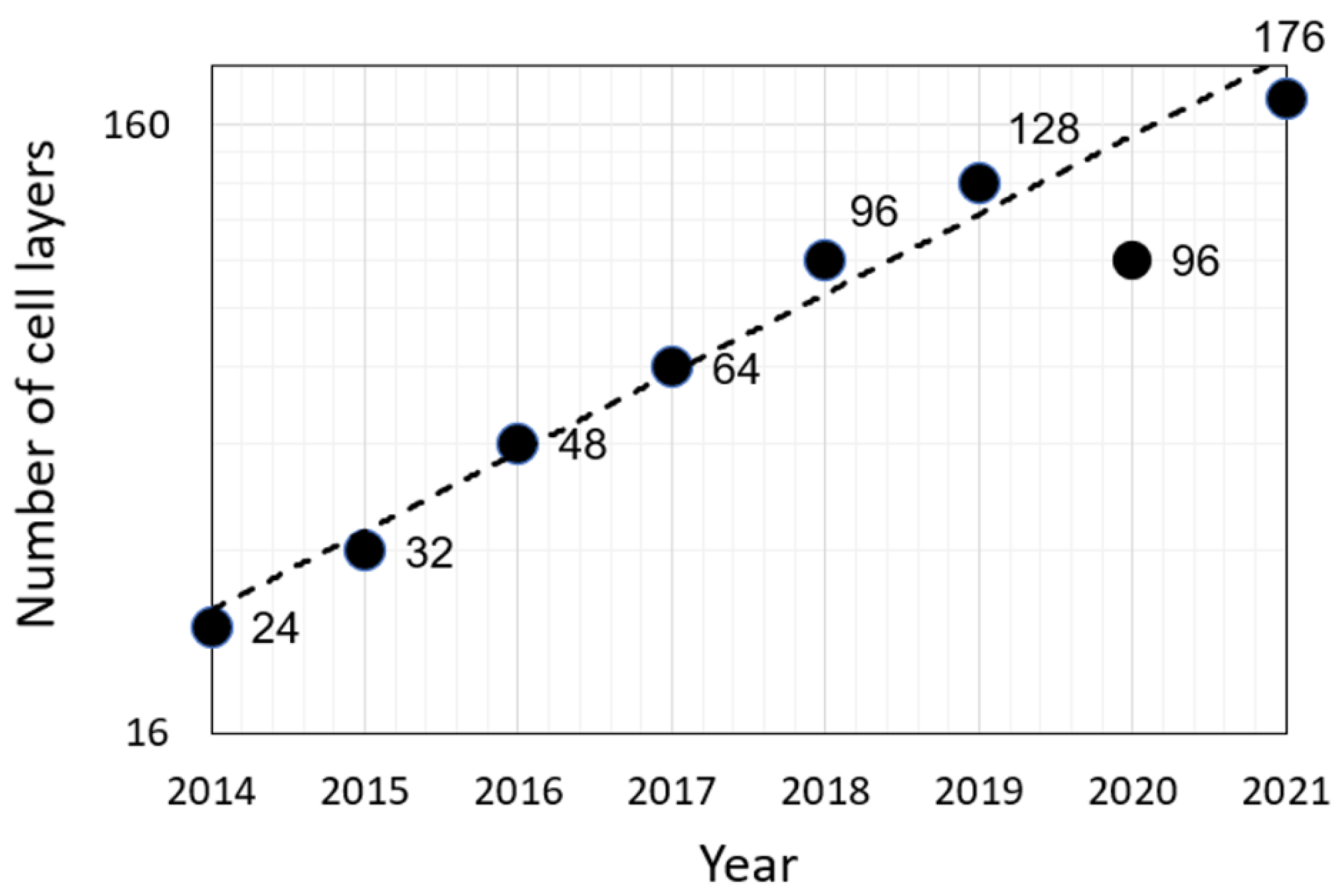
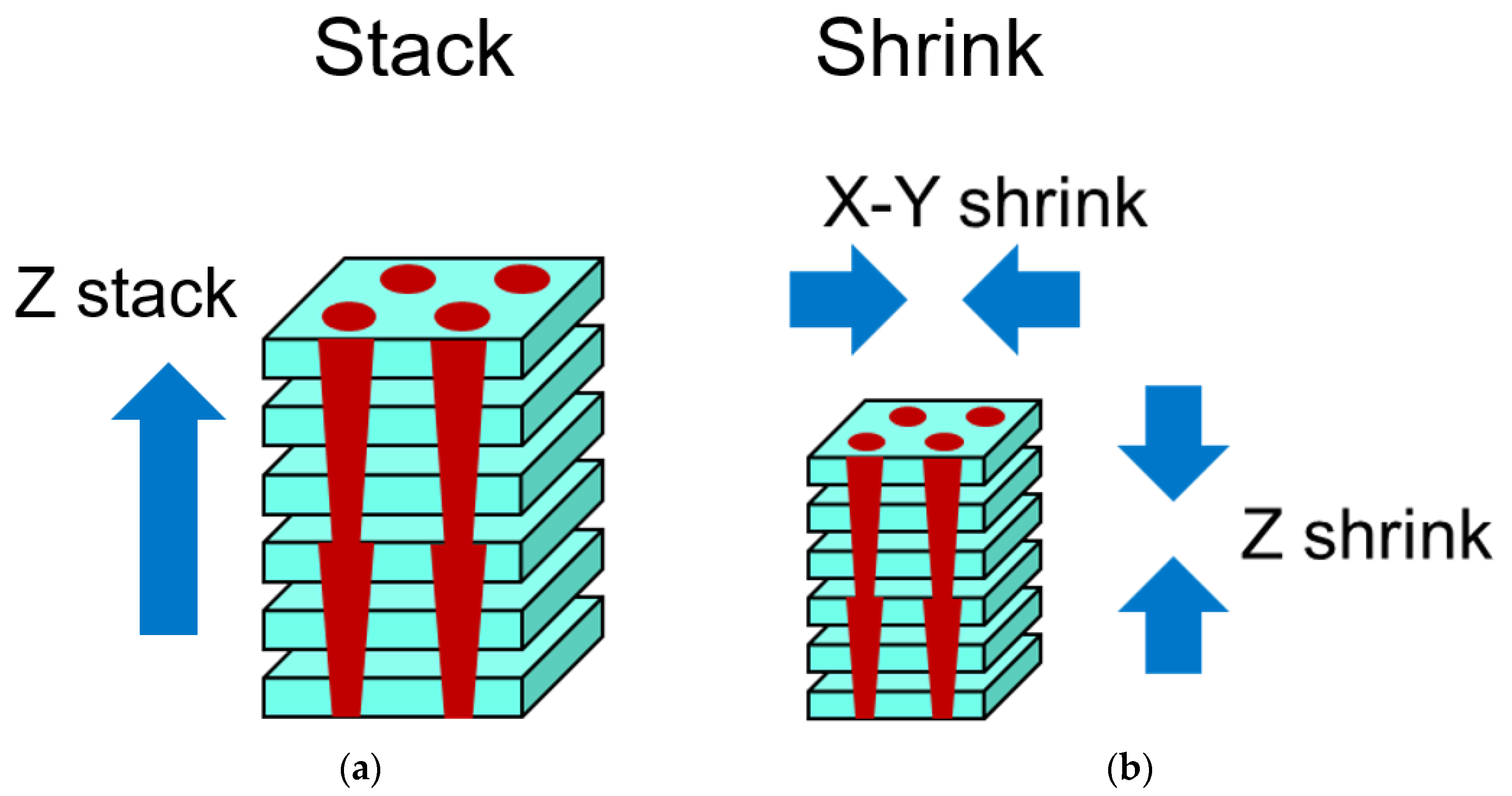
4.1. Conventional Scaling
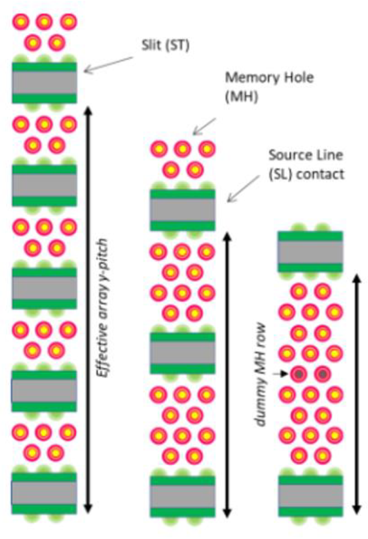
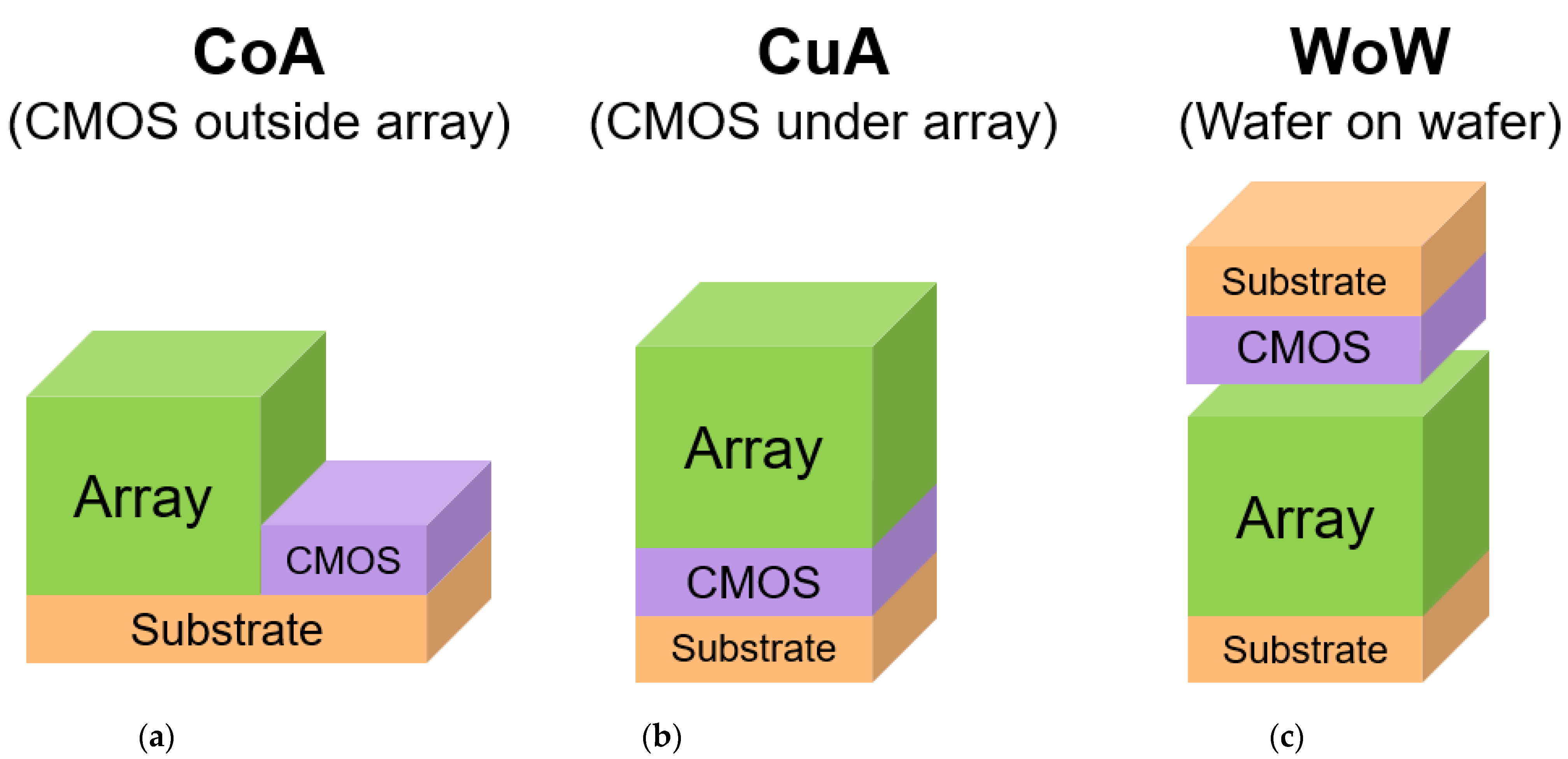
4.2. Disruptive Scaling
5. 3D NAND Array Logical Scaling by Cell Device Engineering
6. 3D NAND Performance Scaling by Design and Algorithms
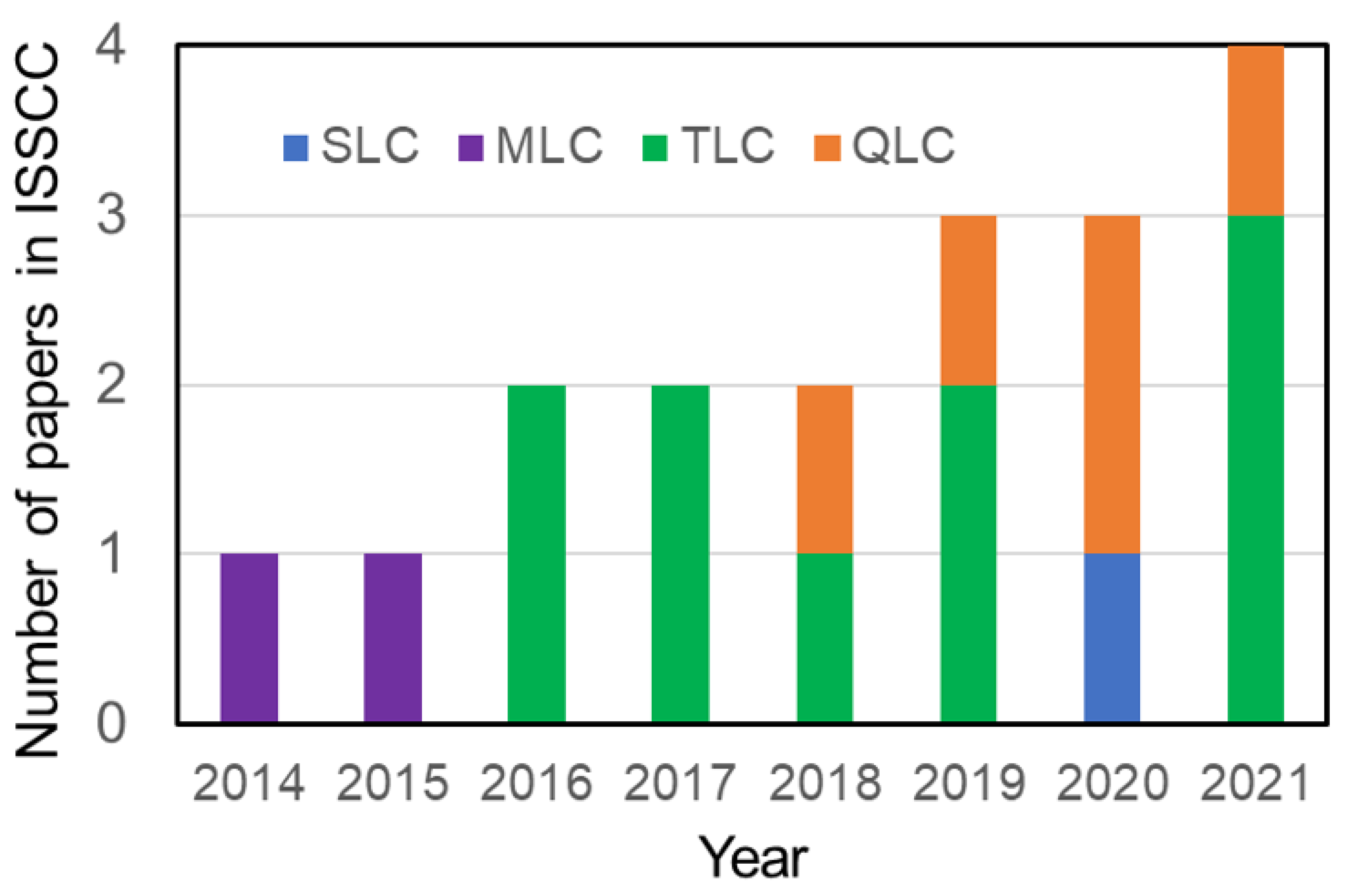
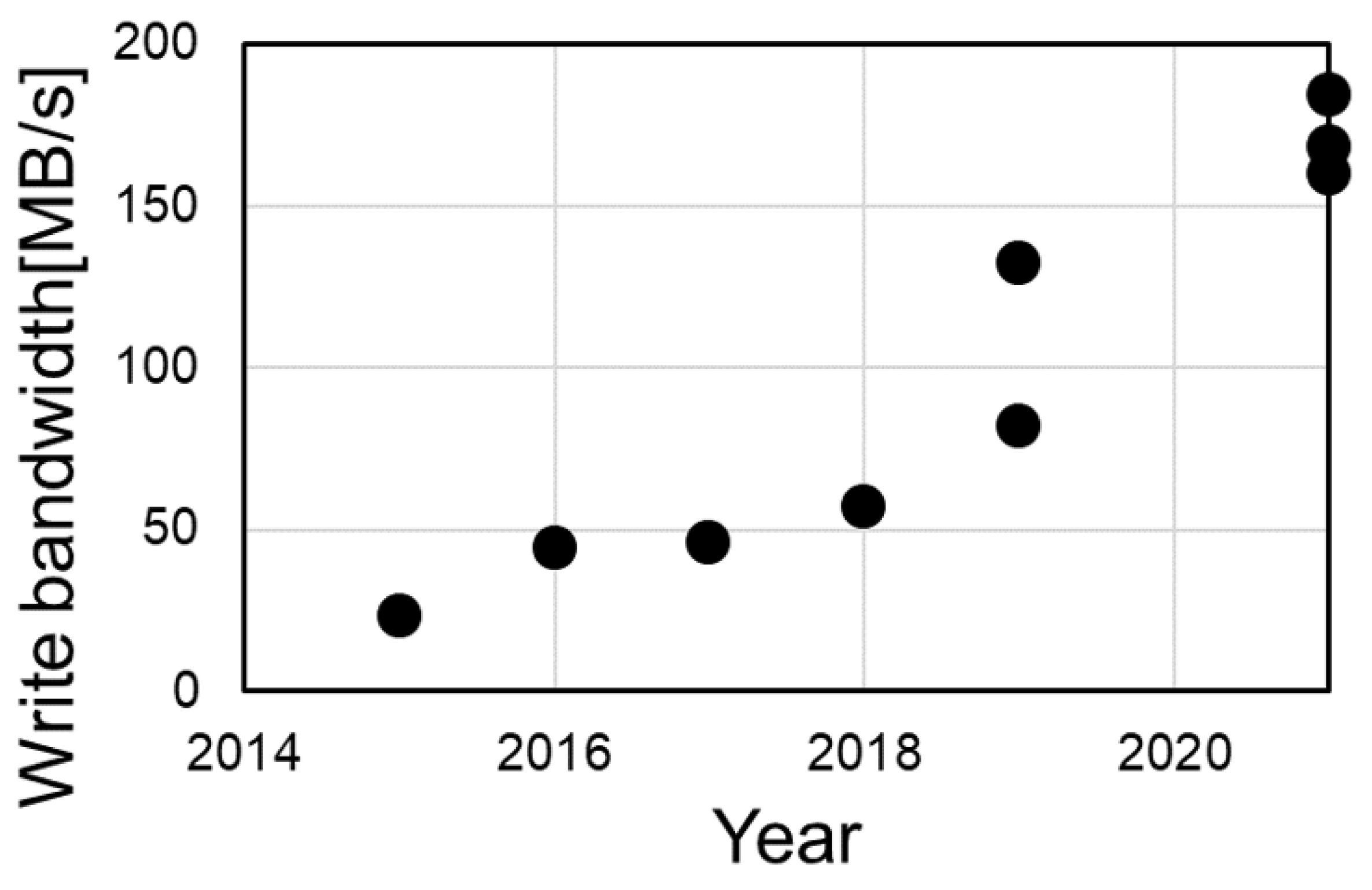
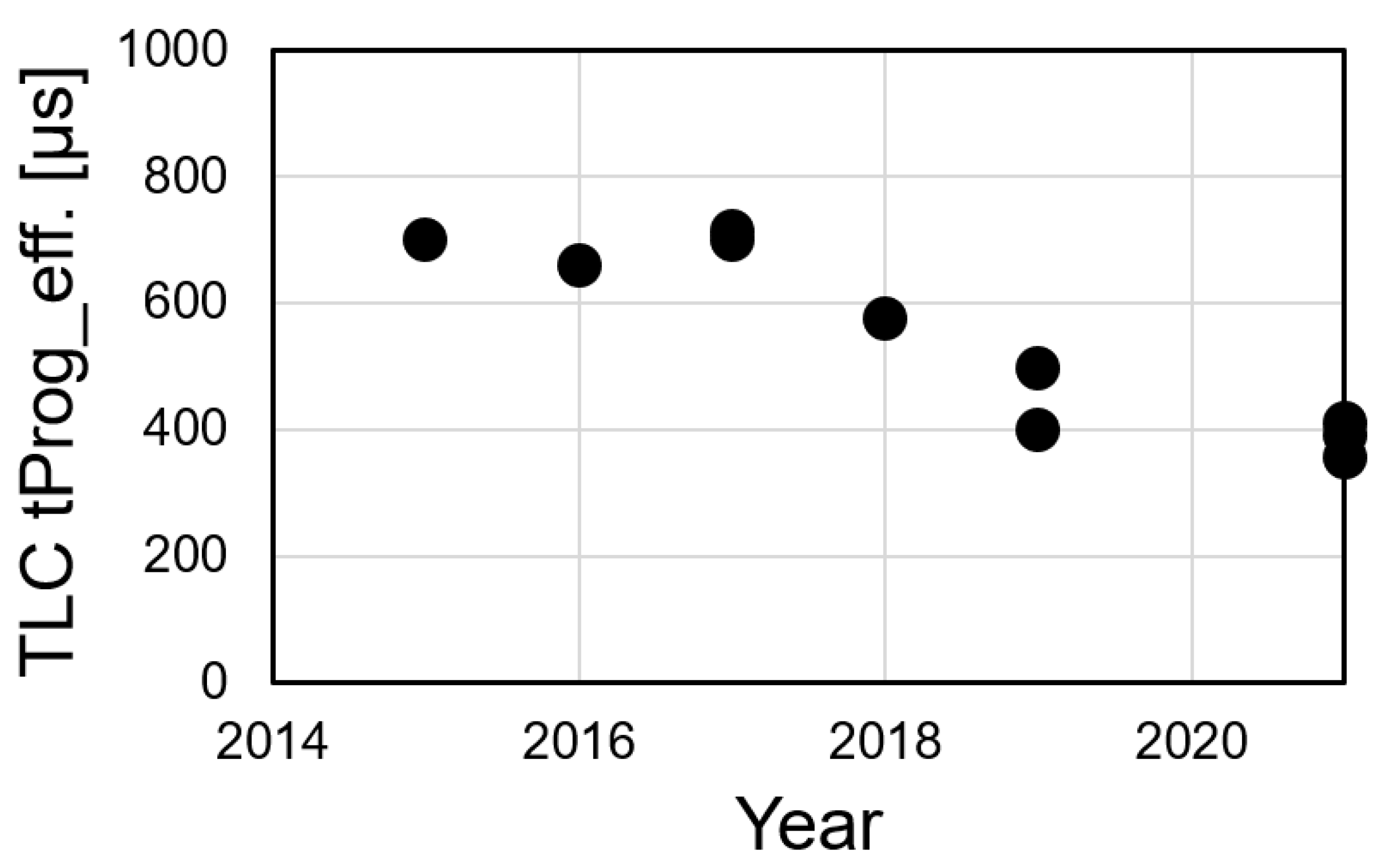
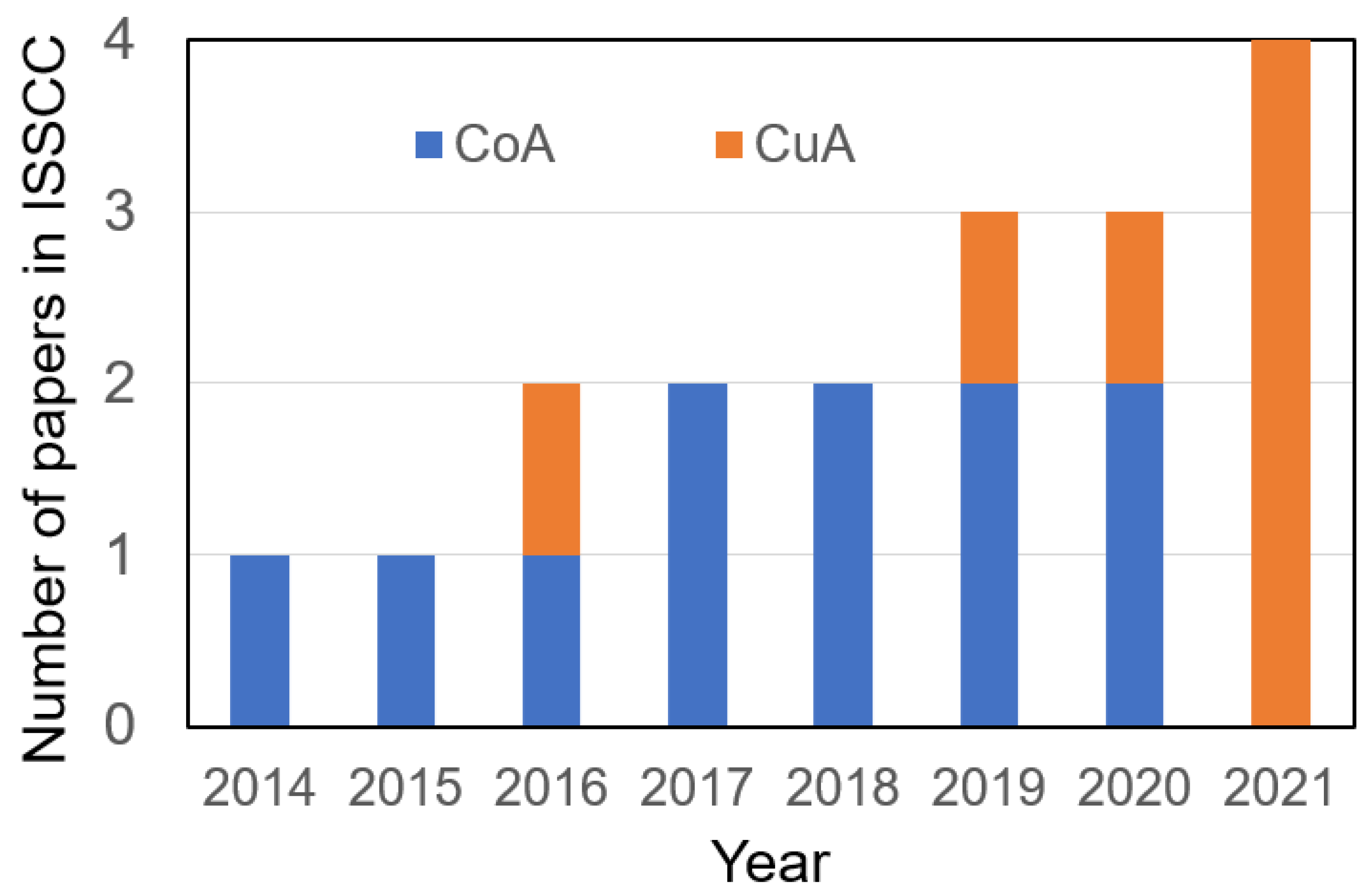
6.1. Write Bandwidth for TLC
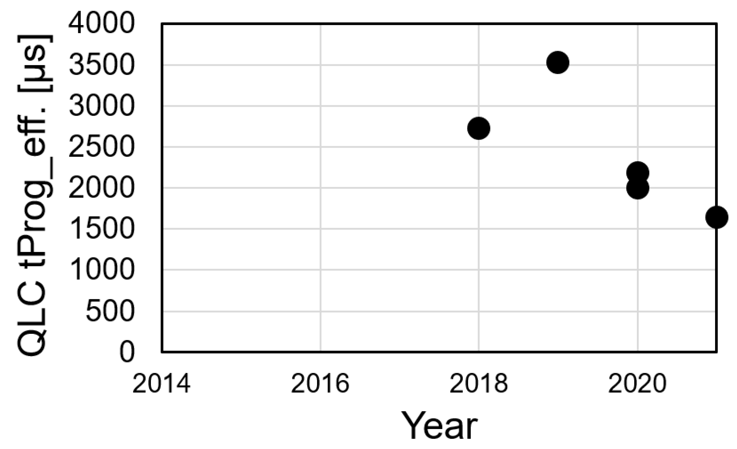
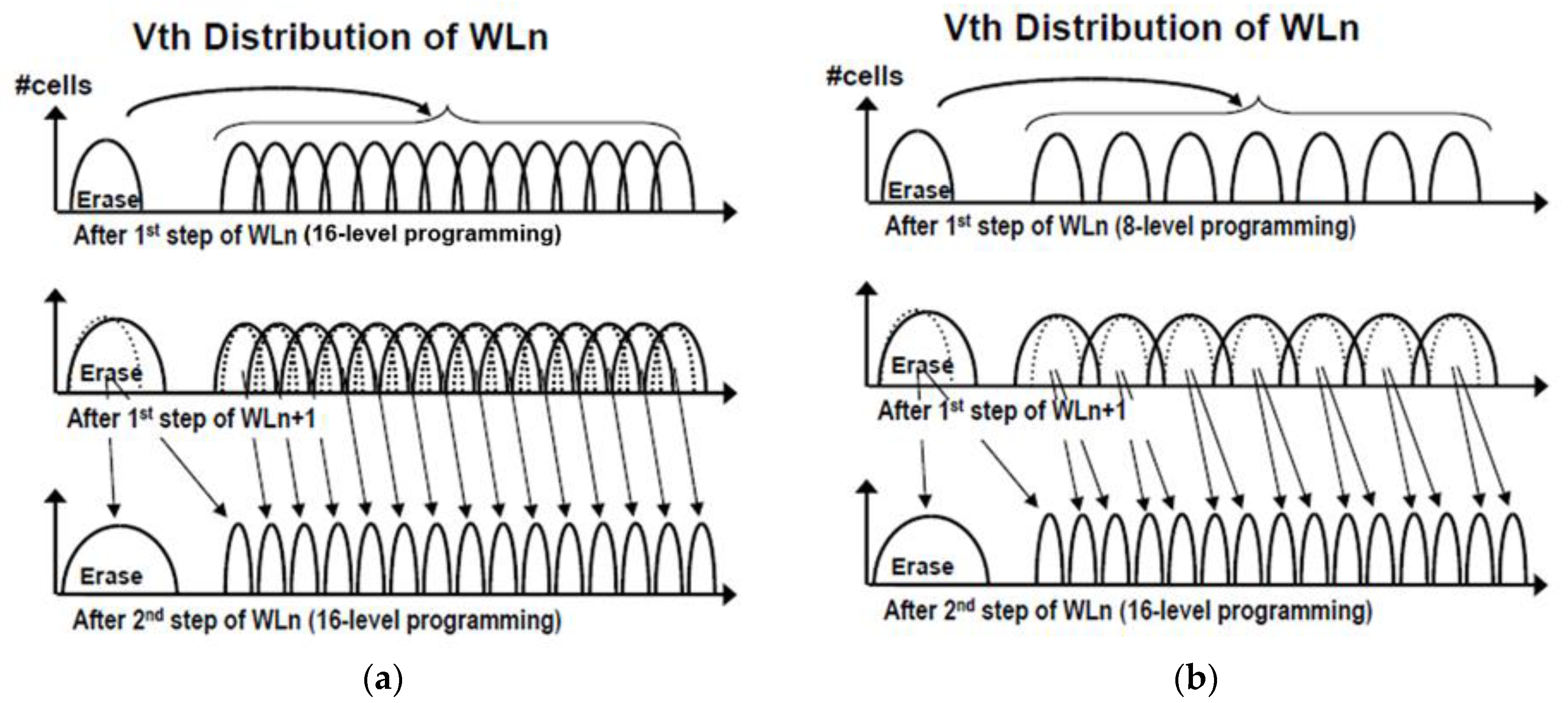
6.2. QLC Program Schemes
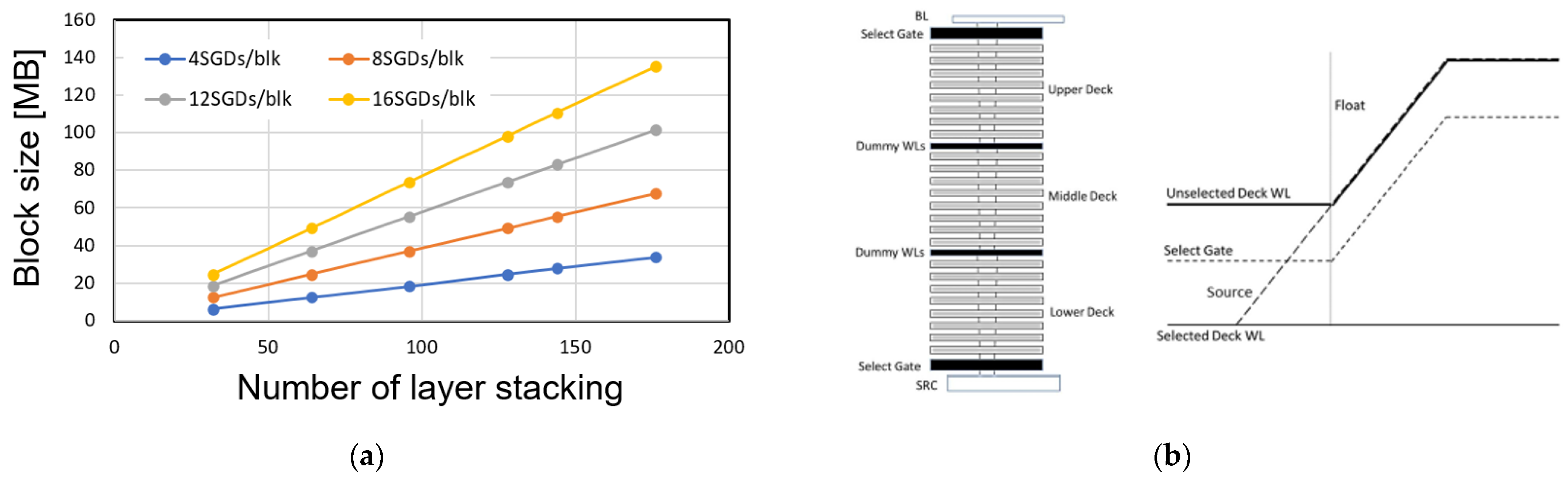
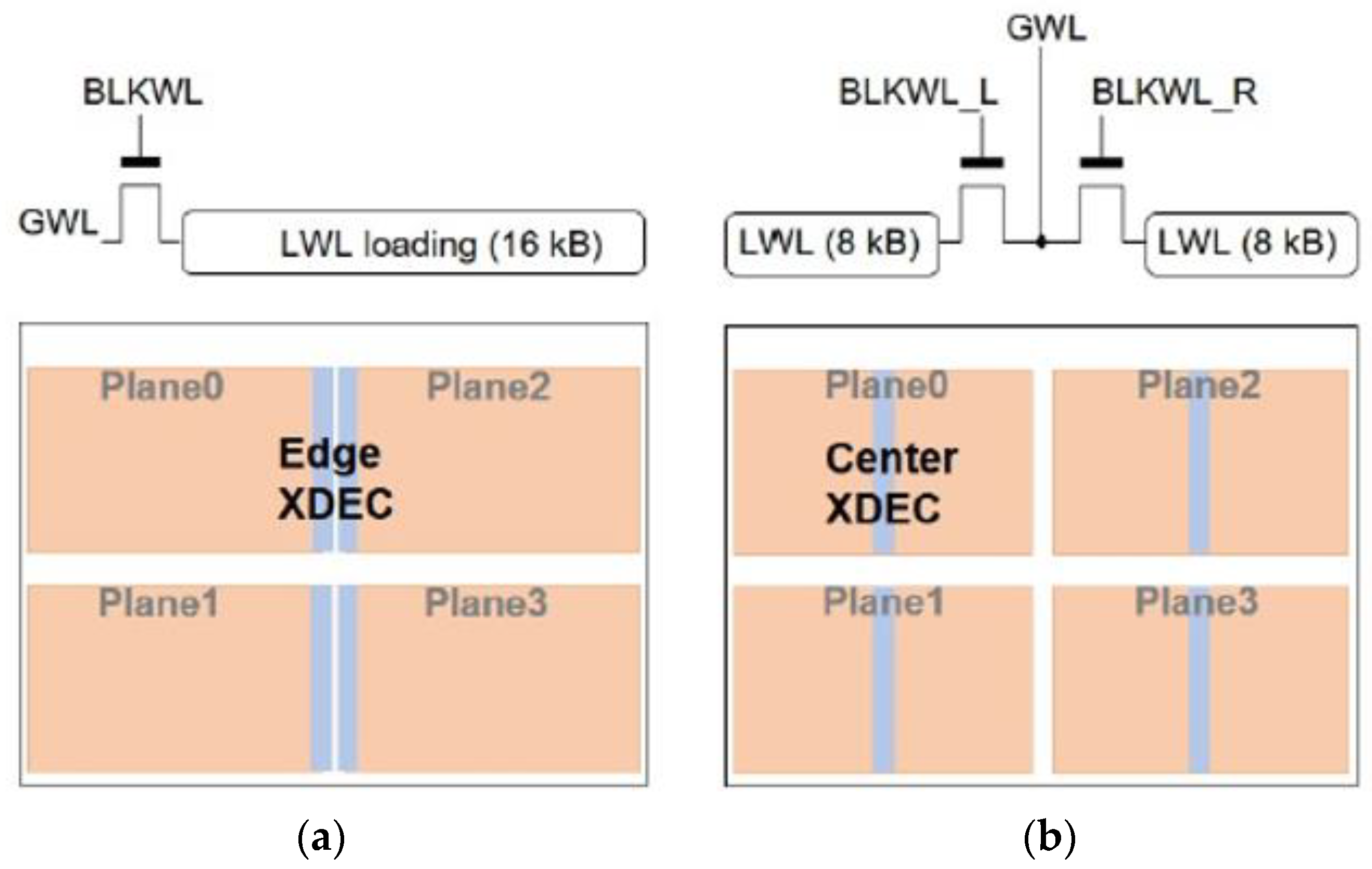
6.3. Block Size Scaling
7. Conclusions
Funding
Conflicts of Interest
References
- Tanaka, H.; Kido, M.; Yahashi, K.; Oomura, M.; Katsumata, R.; Kito, M.; Fukuzumi, Y.; Sato, M.; Nagata, Y.; Matsuoka, Y.; et al. Bit Cost Scalable technology with Punch and plug process for ultra high density flash memory. In Proceedings of the 2007 IEEE Symposium on VLSI Technology, Kyoto, Japan, 12–14 June 2007; pp. 14–15. [Google Scholar] [CrossRef]
- Park, K.T.; Han, J.M.; Kim, D.; Nam, S.; Choi, K.; Kim, M.S.; Kwak, P.; Lee, D.; Choi, Y.H.; Kang, K.M.; et al. Three-dimensional 128 Gb MLC vertical NAND Flash-memory with 24-WL stacked layers and 50 MB/s high-speed programming. In Proceedings of the 2014 IEEE International Solid-State Circuits Conference Digest of Technical Papers (ISSCC), San Francisco, CA, USA, 9–13 February 2014; Volume 57, pp. 334–335. [Google Scholar] [CrossRef]
- Cernea, R.; Pham, L.; Moogat, F.; Chan, S.; Le, B.; Li, Y.; Tsao, S.; Tseng, T.Y.; Nguyen, K.; Li, J.; et al. A 34 MB/s-program-throughput 16 Gb MLC NAND with all-bitline architecture in 56 nm. In Proceedings of the 2008 IEEE International Solid-State Circuits Conference—Digest of Technical Papers, San Francisco, CA, USA, 3–7 February 2008; Volume 51, pp. 420–624. [Google Scholar] [CrossRef]
- Li, Y.; Leo, S.; Fong, Y.; Pan, F.; Kuo, T.C.; Park, J.; Samaddar, T.; Nguyen, H.; Mui, M.; Htoo, K.; et al. A 16 Gb 3 b/Cell NAND flash memory in 56 nm with 8 MB/s write rate. In Proceedings of the 2008 IEEE International Solid-State Circuits Conference—Digest of Technical Papers, San Francisco, CA, USA, 3–7 February 2008; Volume 51, pp. 506–508. [Google Scholar] [CrossRef]
- Kanda, K.; Koyanagi, M.; Yamamura, T.; Hosono, K.; Yoshihara, M.; Miwa, T.; Kato, Y.; Mak, A.; Chan, S.L.; Tsai, F.; et al. A 120 mm2 16 Gb 4-MLC NAND flash memory with 43 nm CMOS technology. In Proceedings of the 2008 IEEE International Solid-State Circuits Conference—Digest of Technical Papers, San Francisco, CA, USA, 3–7 February 2008; Volume 51, pp. 430–625. [Google Scholar] [CrossRef]
- Zeng, R.; Chalagalla, N.; Chu, D.; Elmhurst, D.; Goldman, M.; Haid, C.; Huq, A.; Ichikawa, T.; Jorgensen, J.; Jungroth, O.; et al. A 172 mm2 32 Gb MLC NAND flash memory in 34 nm CMOS. In Proceedings of the 2009 IEEE International Solid-State Circuits Conference—Digest of Technical Papers, San Francisco, CA, USA, 8–12 February 2009; pp. 236–237. [Google Scholar] [CrossRef]
- Trinh, C.; Shibata, N.; Nakano, T.; Ogawa, M.; Sato, J.; Takeyama, Y.; Isobe, K.; Le, B.; Moogat, F.; Mokhlesi, N.; et al. A 5.6 MB/s 64 Gb 4 b/Cell NAND flash memory in 43 nm CMOS. In Proceedings of the 2009 IEEE International Solid-State Circuits Conference—Digest of Technical Papers, San Francisco, CA, USA, 8–12 February 2009; pp. 246–248. [Google Scholar] [CrossRef]
- Futatsuyama, T.; Fujita, N.; Tokiwa, N.; Shindo, Y.; Edahiro, T.; Kamei, T.; Nasu, H.; Iwai, M.; Kato, K.; Fukuda, Y.; et al. A 113 mm2 32 Gb 3 b/cell NAND flash memory. In Proceedings of the 2009 IEEE International Solid-State Circuits Conference—Digest of Technical Papers, San Francisco, CA, USA, 8–12 February 2009; Volume 1, pp. 242–243. [Google Scholar] [CrossRef]
- Lee, C.; Lee, S.K.; Ahn, S.; Lee, J.; Park, W.; Cho, Y.; Jang, C.; Yang, C.; Chung, S.; Yun, I.S.; et al. A 32 Gb MLC NAND-flash memory with Vth-endurance-enhancing schemes in 32 nm CMOS. In Proceedings of the 2010 IEEE International Solid-State Circuits Conference—(ISSCC), San Francisco, CA, USA, 7–11 February 2010; Volume 53, pp. 446–447. [Google Scholar] [CrossRef]
- Marotta, G.G.; Macerola, A.; D’Alessandro, A.; Torsi, A.; Cerafogli, C.; Lattaro, C.; Musilli, C.; Rivers, D.; Sirizotti, E.; Paolini, F.; et al. A 3 bit/Cell 32 Gb NAND flash memory at 34 nm with 6 Mb/s program throughput and with dynamic 2 b/cell blocks configuration mode for a program throughput increase up to 13 MB/s. In Proceedings of the 2010 IEEE International Solid-State Circuits Conference—(ISSCC), San Francisco, CA, USA, 7–11 February 2010; Volume 53, pp. 444–445. [Google Scholar] [CrossRef]
- Kim, H.; Park, J.H.; Park, K.T.; Kwak, P.; Kwon, O.; Kim, C.; Lee, Y.; Park, S.; Kim, K.; Cho, D.; et al. A 159 mm2 32 nm 32 Gb MLC NAND-flash memory with 200 MB/s asynchronous DDR interface. In Proceedings of the 2010 IEEE International Solid-State Circuits Conference—(ISSCC), San Francisco, CA, USA, 7–11 February 2010; Volume 53, pp. 442–443. [Google Scholar] [CrossRef]
- Kim, T.Y.; Lee, S.D.; Park, J.S.; Cho, H.Y.; You, B.S.; Baek, K.H.; Lee, J.H.; Yang, C.W.; Yun, M.; Kim, M.S.; et al. A 32 Gb MLC NAND flash memory with Vth margin-expanding schemes in 26 nm CMOS. In Proceedings of the 2011 IEEE International Solid-State Circuits Conference, San Francisco, CA, USA, 20–24 February 2011; pp. 202–203. [Google Scholar] [CrossRef]
- Park, K.T.; Kwon, O.; Yoon, S.; Choi, M.H.; Kim, I.M.; Kim, B.G.; Kim, M.S.; Choi, Y.H.; Shin, S.H.; Song, Y.; et al. A 7 MB/s 64 Gb 3-bit/cell DDR NAND flash memory in 20 nm-node technology. In Proceedings of the 2011 IEEE International Solid-State Circuits Conference, San Francisco, CA, USA, 20–24 February 2011; Volume 43, pp. 212–213. [Google Scholar] [CrossRef]
- Fukuda, K.; Watanabe, Y.; Makino, E.; Kawakami, K.; Sato, J.; Takagiwa, T.; Kanagawa, N.; Shiga, H.; Tokiwa, N.; Shindo, Y.; et al. A 151 mm2 64 Gb MLC NAND flash memory in 24 nm CMOS technology. In Proceedings of the 2011 IEEE International Solid-State Circuits Conference, San Francisco, CA, USA, 20–24 February 2011; pp. 198–199. [Google Scholar] [CrossRef]
- Lee, D.; Chang, I.J.; Yoon, S.Y.; Jang, J.; Jang, D.S.; Hahn, W.G.; Park, J.Y.; Kim, D.G.; Yoon, C.; Lim, B.S.; et al. A 64 Gb 533 Mb/s DDR interface MLC NAND Flash in sub-20 nm technology. In Proceedings of the 2012 IEEE International Solid-State Circuits Conference, San Francisco, CA, USA, 19–23 February 2012; Volume 55, pp. 430–431. [Google Scholar] [CrossRef]
- Naso, G.; Botticchio, L.; Castelli, M.; Cerafogli, C.; Cichocki, M.; Conenna, P.; D’Alessandro, A.; De Santis, L.; Di Cicco, D.; Di Francesco, W.; et al. A 128 Gb 3 b/cell NAND flash design using 20 nm planar-cell technology. In Proceedings of the 2013 IEEE International Solid-State Circuits Conference Digest of Technical Papers, San Francisco, CA, USA, 17–21 February 2013; Volume 56, pp. 218–219. [Google Scholar] [CrossRef]
- Helm, M.; Park, J.K.; Ghalam, A.; Guo, J.; Ha, C.W.; Hu, C.; Kim, H.; Kavalipurapu, K.; Lee, E.; Mohammadzadeh, A.; et al. A 128 Gb MLC NAND-Flash device using 16 nm planar cell. In Proceedings of the 2014 IEEE International Solid-State Circuits Conference Digest of Technical Papers, San Francisco, CA, USA, 9–13 February 2014; Volume 57, pp. 326–327. [Google Scholar] [CrossRef]
- Choi, S.; Kim, D.; Choi, S.; Kim, B.; Jung, S.; Chun, K.; Kim, N.; Lee, W.; Shin, T.; Jin, H.; et al. A 93.4 mm2 64 Gb MLC NAND-flash memory with 16 nm CMOS technology. In Proceedings of the 2014 IEEE International Solid-State Circuits Conference Digest of Technical Papers, San Francisco, CA, USA, 9–13 February 2014; Volume 57, pp. 328–329. [Google Scholar] [CrossRef]
- Sako, M.; Watanabe, Y.; Nakajima, T.; Sato, J.; Muraoka, K.; Fujiu, M.; Kouno, F.; Nakagawa, M.; Masuda, M.; Kato, K.; et al. A low-power 64 Gb MLC NAND-flash memory in 15 nm CMOS technology. In Proceedings of the 2015 IEEE International Solid-State Circuits Conference Digest of Technical Papers, San Francisco, CA, USA, 22–26 February 2015; Volume 58, pp. 128–129. [Google Scholar] [CrossRef]
- Im, J.W.; Jeong, W.P.; Kim, D.H.; Nam, S.W.; Shim, D.K.; Choi, M.H.; Yoon, H.J.; Kim, D.H.; Kim, Y.S.; Park, H.W.; et al. A 128 Gb 3 b/cell V-NAND flash memory with 1 Gb/s I/O rate. In Proceedings of the 2015 IEEE International Solid-State Circuits Conference Digest of Technical Papers, San Francisco, CA, USA, 22–26 February 2015; Volume 58, pp. 130–131. [Google Scholar] [CrossRef]
- Tanaka, T.; Helm, M.; Vali, T.; Ghodsi, R.; Kawai, K.; Park, J.K.; Yamada, S.; Pan, F.; Einaga, Y.; Ghalam, A.; et al. A 768 Gb 3 b/cell 3D-floating-gate NAND flash memory. In Proceedings of the 2016 IEEE International Solid-State Circuits Conference (ISSCC), San Francisco, CA, USA, 31 January–4 February 2016; Volume 59, pp. 142–144. [Google Scholar] [CrossRef]
- Yamashita, R.; Magia, S.; Higuchi, T.; Yoneya, K.; Yamamura, T.; Mizukoshi, H.; Zaitsu, S.; Yamashita, M.; Toyama, S.; Kamae, N.; et al. A 51 2Gb 3 b/cell flash memory on 64-word-line-layer BiCS technology. In Proceedings of the 2017 IEEE International Solid-State Circuits Conference (ISSCC), San Francisco, CA, USA, 5–9 February 2017; Volume 60, pp. 196–197. [Google Scholar] [CrossRef]
- Kim, C.; Cho, J.H.; Jeong, W.; Park, I.H.; Park, H.W.; Kim, D.H.; Kang, D.; Lee, S.; Lee, J.S.; Kim, W.; et al. A 512 Gb 3 b/cell 64-stacked WL 3D V-NAND flash memory. In Proceedings of the 2017 IEEE International Solid-State Circuits Conference (ISSCC), San Francisco, CA, USA, 5–9 February 2017; Volume 60, pp. 202–203. [Google Scholar] [CrossRef]
- Lee, S.; Kim, C.; Kim, M.; Joe, S.M.; Jang, J.; Kim, S.; Lee, K.; Kim, J.; Park, J.; Lee, H.J.; et al. A 1 Tb 4 b/cell 64-stacked-WL 3D NAND flash memory with 12 MB/s program throughput. In Proceedings of the 2018 IEEE International Solid—State Circuits Conference—(ISSCC), San Francisco, CA, USA, 11–15 February 2018; Volume 61, pp. 340–342. [Google Scholar] [CrossRef]
- Maejima, H.; Kanda, K.; Fujimura, S.; Takagiwa, T.; Ozawa, S.; Sato, J.; Shindo, Y.; Sato, M.; Kanagawa, N.; Musha, J.; et al. A 512 Gb 3 b/Cell 3D flash memory on a 96-word-line-layer technology. In Proceedings of the 2018 IEEE International Solid—State Circuits Conference—(ISSCC), San Francisco, CA, USA, 11–15 February 2018; Volume 61, pp. 336–338. [Google Scholar] [CrossRef]
- Sugawara, H.; Hosono, K.; Hisada, T.; Kaneko, T.; Nakamura, H. A 1.33 Tb 4-bit/Cell 3D-Flash Memory on a 96-Word-Line-Layer Technology. In Proceedings of the 2019 IEEE International Solid-State Circuits Conference—(ISSCC), San Francisco, CA, USA, 17–21 February 2019; Volume 43, pp. 210–212. [Google Scholar]
- Siau, C.; Kim, K.H.; Lee, S.; Isobe, K.; Shibata, N.; Verma, K.; Ariki, T.; Li, J.; Yuh, J.; Amarnath, A.; et al. A 512 Gb 3-bit/Cell 3D Flash Memory on 128-Wordline-Layer with 132 MB/s Write Performance Featuring Circuit-Under-Array Technology. In Proceedings of the 2019 IEEE International Solid-State Circuits Conference—(ISSCC), San Francisco, CA, USA, 17–21 February 2019; pp. 218–220. [Google Scholar] [CrossRef]
- Higuchi, T.; Kodama, T.; Kato, K.; Fukuda, R.; Tokiwa, N.; Abe, M.; Takagiwa, T.; Shimizu, Y. A 1 Tb 3 b/Cell 3D-Flash Memory in a 170+ Word-Line-Layer Technology. In Proceedings of the 2021 IEEE International Solid-State Circuits Conference (ISSCC), San Francisco, CA, USA, 13–22 February 2021; pp. 428–430. [Google Scholar]
- Huh, H.; Cho, W.; Lee, J.; Noh, Y.; Park, Y.; Ok, S.; Kim, J.; Cho, K.; Lee, H.; Kim, G.; et al. A 1 Tb 4 b/Cell 96-Stacked-WL 3D NAND Flash Memory with 30 MB/s Program Throughput Using Peripheral Circuit under Memory Cell Array Technique. In Proceedings of the 2020 IEEE International Solid-State Circuits Conference—(ISSCC), San Francisco, CA, USA, 16–20 February 2021; pp. 220–221. [Google Scholar] [CrossRef]
- Khakifirooz, A.; Balasubrahmanyam, S.; Fastow, R.; Gaewsky, K.H.; Ha, C.W.; Haque, R.; Jungroth, O.W.; Law, S.; Madraswala, A.S.; Ngo, B.; et al. A 1 Tb 4 b/Cell 144-Tier Floating-Gate 3D-NAND Flash Memory with 40 MB/s Program Throughput and 13.8 Gb/mm2 Bit Density. In Proceedings of the 2021 IEEE International Solid-State Circuits Conference (ISSCC), San Francisco, CA, USA, 16–20 February 2021; Volume 64, pp. 424–426. [Google Scholar] [CrossRef]
- Park, J.; Kim, D.; Ok, S.; Park, J.; Kwon, T.; Lee, H.; Lim, S.; Jung, S.; Choi, H.; Kang, T.; et al. A 176-Stacked 512 Gb 3 b/Cell 3D-NAND Flash with 10.8 Gb/mm2 Density with a Peripheral Circuit Under Cell Array Architecture. In Proceedings of the 2021 IEEE International Solid-State Circuits Conference (ISSCC), San Francisco, CA, USA, 13–22 February 2021; pp. 422–423. [Google Scholar]
- Lee, G.H.; Hwang, S.; Yu, J.; Kim, H. Architecture and process integration overview of 3d nand flash technologies. Appl. Sci. 2021, 11, 6073. [Google Scholar] [CrossRef]
- Parat, K.; Dennison, C. A floating gate based 3D NAND technology with CMOS under array. In Proceedings of the 2015 IEEE International Electron Devices Meeting (IEDM), Washington, DC, USA, 7–9 December 2015; pp. 3.3.1–3.3.4. [Google Scholar] [CrossRef]
- Goda, A. 3-D NAND Technology Achievements and Future Scaling Perspectives. IEEE Trans. Electron Devices 2020, 67, 1373–1381. [Google Scholar] [CrossRef]
- Hemink, G.; Goda, A. NAND technology status and perspectives. In Semiconductor Memories and Systems; Redaelli, A., Pellizzer, F., Eds.; Elsevier: Amsterdam, The Netherlands, 2022; in press. [Google Scholar]
- Jang, J.; Kim, H.S.; Cho, W.; Cho, H.; Kim, J.; Sun, I.S.; Jang, Y.; Jeong, J.H.; Son, B.K.; Dong, W.K.; et al. Vertical cell array using TCAT(terabit cell array transistor) technology for ultra high density NAND flash memory. In Proceedings of the 2009 Symposium on VLSI Technology, Kyoto, Japan, 15–17 June 2019; pp. 192–193. [Google Scholar]
- Lue, H.T.; Wang, S.Y.; Lai, E.K.; Shih, Y.H.; Lai, S.C.; Yang, L.W.; Chen, K.C.; Ku, J.; Hsieh, K.Y.; Liu, R.; et al. BE-SONOS: A bandgap engineered SONOS with excellent performance and reliability. In Proceedings of the IEEE International Electron Devices Meeting, Washington, DC, USA, 5 December 2005; pp. 547–550. [Google Scholar] [CrossRef]
- Park, Y.; Choi, J.; Kang, C.; Lee, C.; Shin, Y.; Choi, B.; Kim, J.; Jeon, S.; Sel, J.; Park, J.; et al. Highly manufacturable 32 Gb multi—Level NAND flash memory with 0.0098 μm2 cell size using TANOS(Si—Oxide—Al2O3—TaN) cell technology. In Proceedings of the 2006 International Electron Devices Meeting, San Francisco, CA, USA, 11–13 December 2006; Volume 2, pp. 5–8. [Google Scholar] [CrossRef]
- Chen, C.P.; Lue, H.T.; Hsieh, C.C.; Chang, K.P.; Hsieh, K.Y.; Lu, C.Y. Study of fast initial charge loss and it’s impact on the programmed states Vt distribution of charge-trapping NAND flash. In Proceedings of the 2010 International Electron Devices Meeting, San Francisco, CA, USA, 6–8 December 2010; pp. 118–121. [Google Scholar] [CrossRef]
- Woo, C.; Kim, S.; Park, J.; Shin, H.; Kim, H.; Choi, G.B.; Seo, M.S.; Noh, K.H. Modeling of Charge Failure Mechanisms during the Short Term Retention Depending on Program/Erase Cycle Counts in 3-D NAND Flash Memories. In Proceedings of the 2020 IEEE International Reliability Physics Symposium (IRPS), Dallas, TX, USA, 28 April–30 May 2020; pp. 3–8. [Google Scholar] [CrossRef]
- Alsmeier, J.; Higashitani, M.; Paak, S.S.; Sivaram, S. Past and future of 3D flash. In Proceedings of the 2020 IEEE International Electron Devices Meeting (IEDM), San Francisco, CA, USA, 12–18 December 2020; pp. 6.1.1–6.1.4. [Google Scholar] [CrossRef]
- Lue, H.T.; Hsu, T.H.; Wu, C.J.; Chen, W.C.; Yeh, T.H.; Chang, K.P.; Hsieh, C.C.; Du, P.Y.; Hsiao, Y.H.; Jiang, Y.W.; et al. A novel double-density, single-gate vertical channel (SGVC) 3D NAND Flash that is tolerant to deep vertical etching CD variation and possesses robust read-disturb immunity. In Proceedings of the 2015 IEEE International Electron Devices Meeting (IEDM), Washington, DC, USA, 7–9 December 2015; pp. 3.2.1–3.2.4. [Google Scholar] [CrossRef]
- Fujiwara, M.; Ishikawa, T.; Arayashiki, Y.; Hirayama, K.; Koyama, Y.; Kashiyama, S.; Cai, W.; Goki, Y.; Sawa, K.; Ikeno, D.; et al. 3D Semicircular Flash Memory Cell: Novel Split-Gate Technology to Boost Bit Density. In Proceedings of the 2019 IEEE International Electron Devices Meeting (IEDM), San Francisco, CA, USA, 7–12 December 2019; pp. 642–645. [Google Scholar] [CrossRef]
- Ishimaru, K. Future of Non-Volatile Memory -From Storage to Computing. Procedding of the 2019 IEEE International Electron Devices Meeting (IEDM), San Francisco, CA, USA, 7–12 December 2019; pp. 12–17. [Google Scholar] [CrossRef]
- Fu, C.H.; Lue, H.T.; Hsu, T.H.; Chen, W.C.; Lee, G.R.; Chiu, C.J.; Wang, K.C.; Lu, C.Y. A Novel Confined Nitride-Trapping Layer Device for 3D NAND Flash with Robust Retention Performances. In Proceedings of the 2019 Symposium on VLSI Technology, Kyoto, Japan, 9–14 June 2019. [Google Scholar] [CrossRef]
- Kalavade, P. 4 bits/cell 96 Layer Floating Gate 3D NAND with CMOS under Array Technology and SSDs. In Proceedings of the 2020 IEEE International Memory Workshop (IMW), Dresden, Germany, 17–20 May 2020; pp. 14–17. [Google Scholar] [CrossRef]
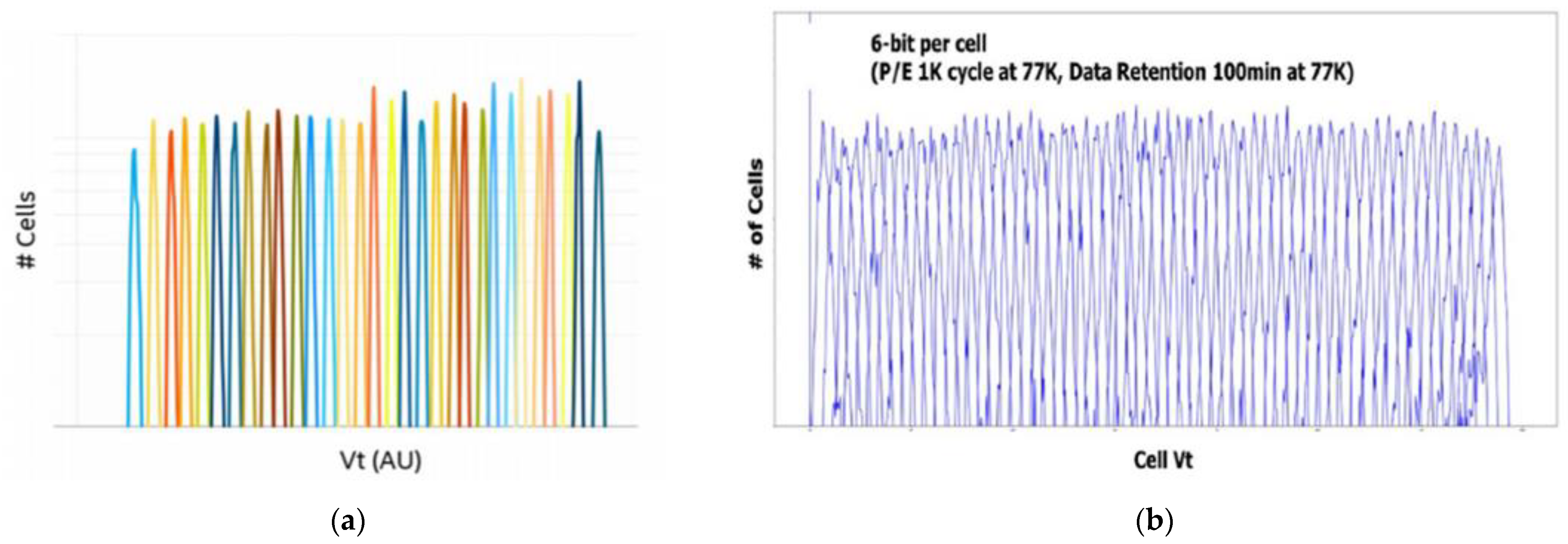
- Aiba, Y.; Tanaka, H.; Maeda, T.; Sawa, K.; Kikushima, F.; Miura, M.; Fujisawa, T.; Matsuo, M.; Sanuki, T. Cryogenic Operation of 3D Flash Memory for New Applications and Bit Cost Scaling with 6-Bit per Cell (HLC) and beyond. In Proceedings of the 2021 5th IEEE Electron Devices Technology & Manufacturing Conference (EDTM), Chengdu, China, 8–11 April 2021; pp. 28–30. [Google Scholar] [CrossRef]
- Yang, S. Unleashing 3D NAND’s Potential with an Innovative Architecture. In Proceedings of the Flash Memory Summit, Santa Clara, CA, USA, 7 August 2018. [Google Scholar]


Publisher’s Note: MDPI stays neutral with regard to jurisdictional claims in published maps and institutional affiliations. |
© 2021 by the author. Licensee MDPI, Basel, Switzerland. This article is an open access article distributed under the terms and conditions of the Creative Commons Attribution (CC BY) license (https://creativecommons.org/licenses/by/4.0/).
Share and Cite
Goda, A. Recent Progress on 3D NAND Flash Technologies. Electronics 2021, 10, 3156. https://doi.org/10.3390/electronics10243156
Goda A. Recent Progress on 3D NAND Flash Technologies. Electronics. 2021; 10(24):3156. https://doi.org/10.3390/electronics10243156
Chicago/Turabian StyleGoda, Akira. 2021. "Recent Progress on 3D NAND Flash Technologies" Electronics 10, no. 24: 3156. https://doi.org/10.3390/electronics10243156
APA StyleGoda, A. (2021). Recent Progress on 3D NAND Flash Technologies. Electronics, 10(24), 3156. https://doi.org/10.3390/electronics10243156