
Impact of Residual Stress on a Polysilicon Channel in Scaled 3D NAND Flash Memory


Abstract
:1. Introduction
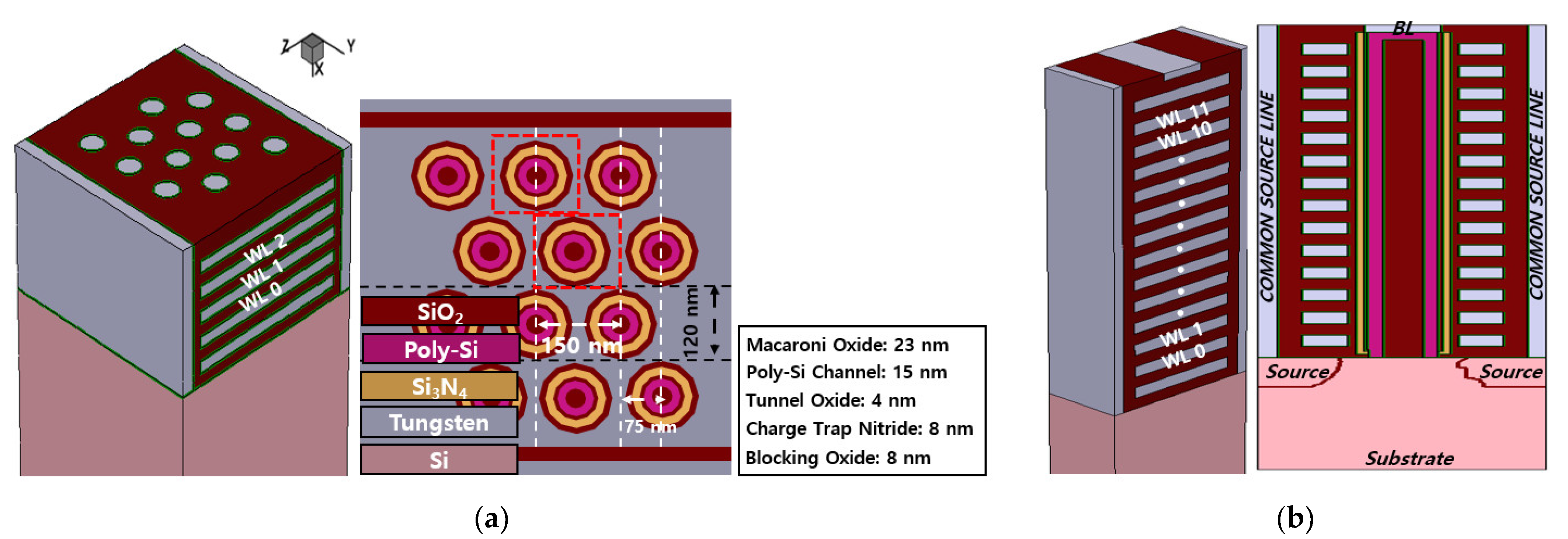
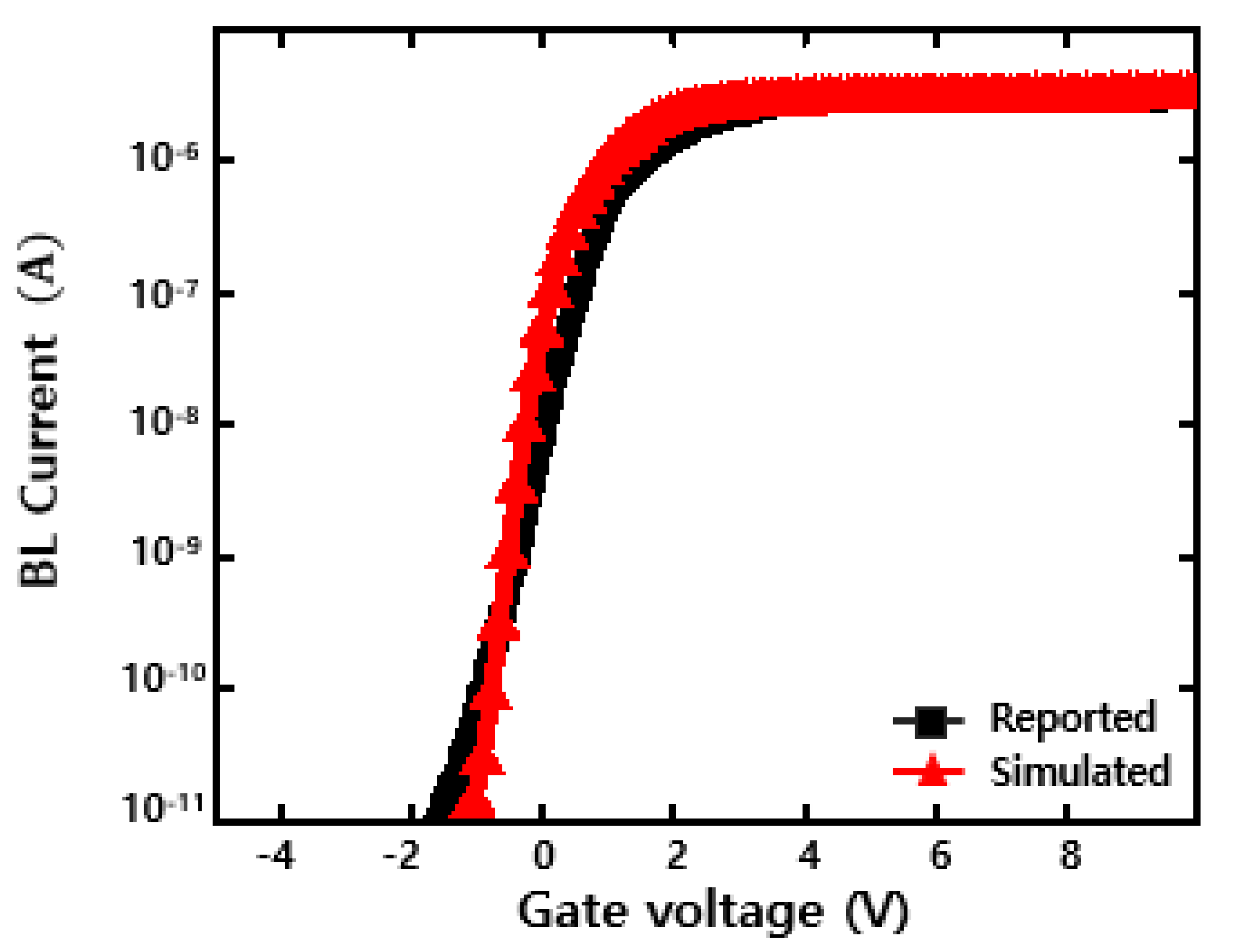
2. Materials and Methods
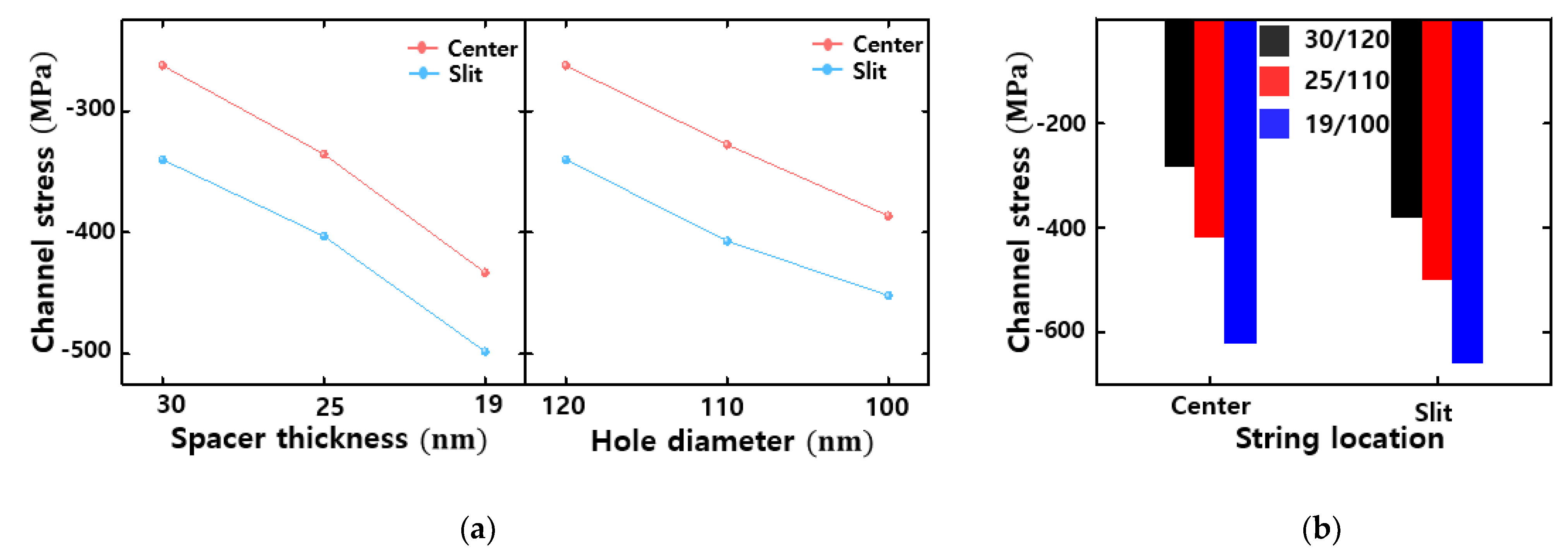
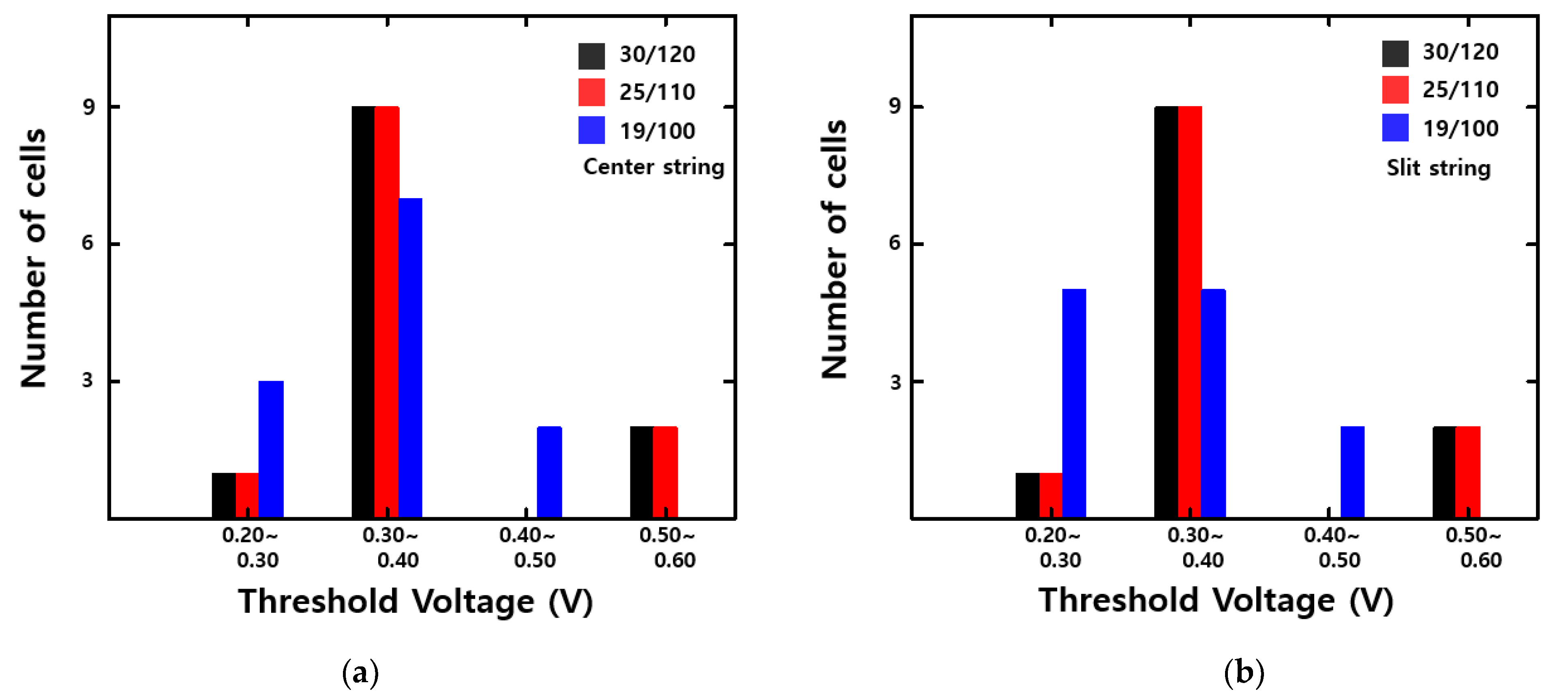
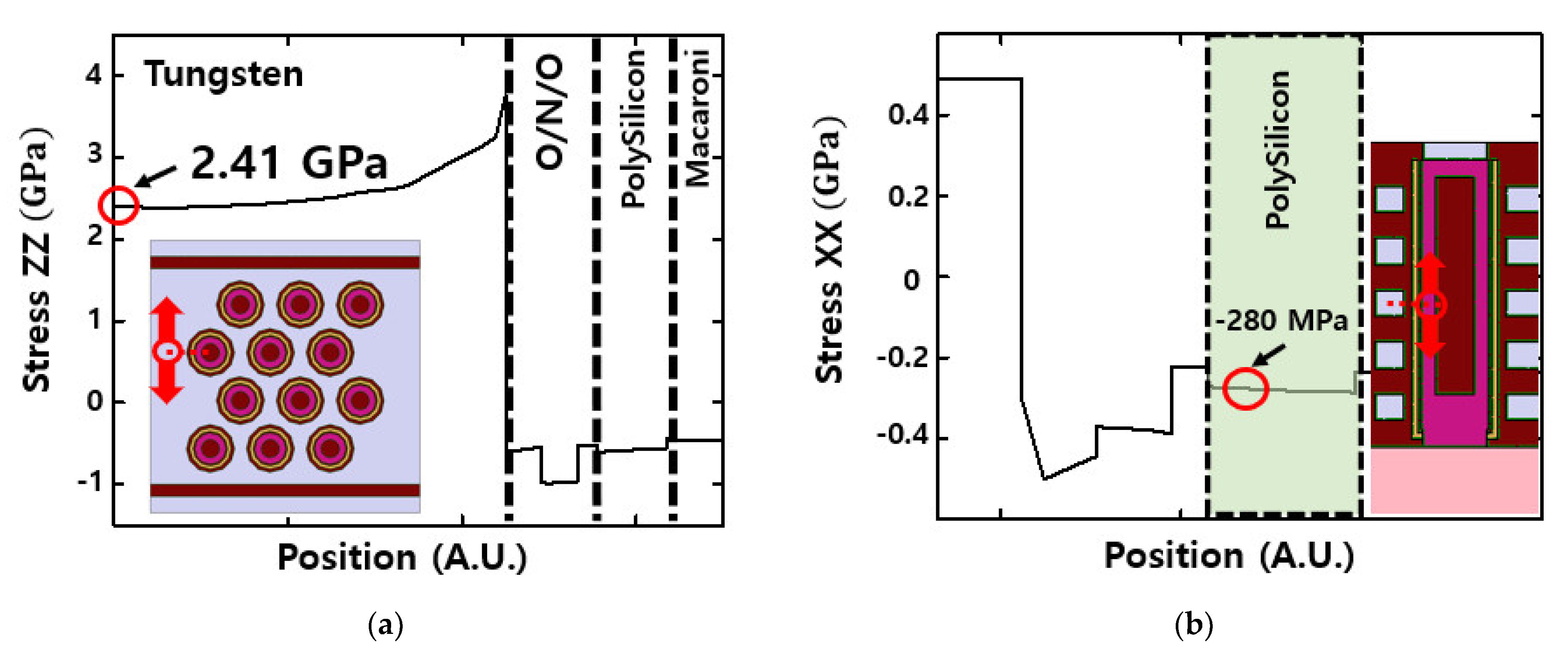
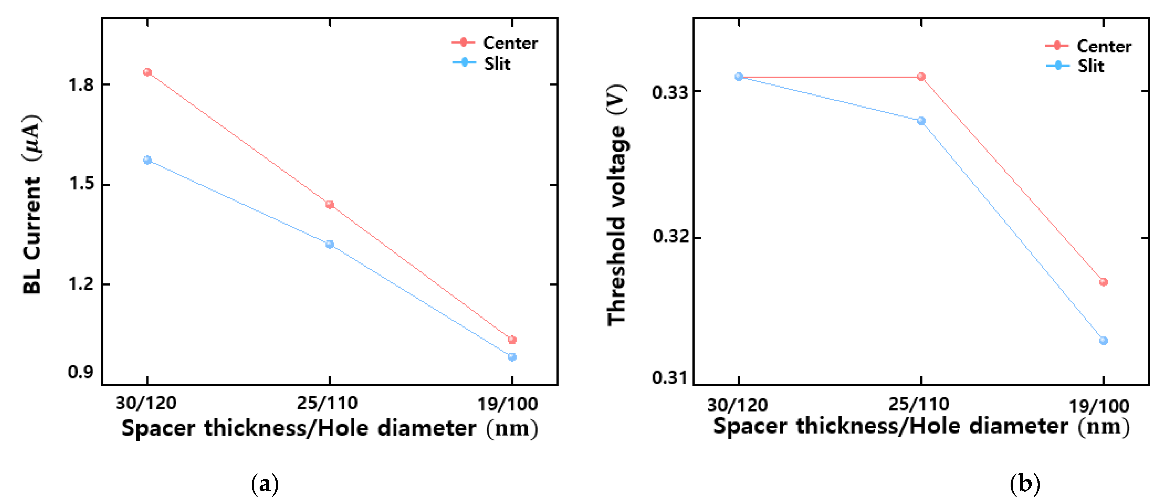
3. Results and Discussion
Impact of Scaling on the Residual Stress of the Polysilicon Channel
4. Conclusions
Author Contributions
Funding
Acknowledgments
Conflicts of Interest
References
- Siau, C.; Kim, K.H.; Lee, S.; Isobe, K.; Shibata, N.; Verma, K.; Ariki, T.; Li, J.; Yuh, J.; Amarnath, A.; et al. 13.5 A 512Gb 3-bit/Cell 3D Flash Memory on 128-Wordline-Layer with 132 MB/s Write Performance Featuring Circuit-Under-Array Technology. In Proceedings of the 2019 IEEE International Solid-State Circuits Conference—(ISSCC), San Francisco, CA, USA, 17–21 February 2019; pp. 218–220. [Google Scholar]
- Goda, A. 3-D NAND Technology Achievements and Future Scaling Perspectives. IEEE Trans. Electron Devices 2020, 67, 1373–1381. [Google Scholar] [CrossRef]
- Kim, H.; Ahn, S.; Shin, Y.G.; Lee, K.; Jung, E. Evolution of NAND Flash Memory: From 2D to 3D as a Storage Market Leader. In Proceedings of the 2017 IEEE International Memory Workshop (IMW), Monterey, CA, USA, 14–17 May 2017; pp. 1–4. [Google Scholar]
- Parat, K.; Goda, A. Scaling Trends in NAND Flash. In Proceedings of the 2018 IEEE International Electron Devices Meeting (IEDM), San Francisco, CA, USA, 1–5 December 2018; pp. 2.1.1–2.1.4. [Google Scholar]
- Lee, S. Technology scaling challenges and opportunities of memory devices. In Proceedings of the 2016 IEEE International Electron Devices Meeting (IEDM), San Francisco, CA, USA, 3–7 December 2016; pp. 1.1.1–1.1.8. [Google Scholar]
- Kim, J.H.; Lim, J.; Kim, H.S.; Cho, E.S.; Yeo, C.; Lee, W.; You, B.; Lee, B.; Kang, M.; Jang, W.; et al. Highly Manufacturable 7th Generation 3D NAND Flash Memory with COP structure and Double Stack Process. In Proceedings of the 2021 VLSI Symposium Technology, Kyoto, Japan, 13–19 June 2021. [Google Scholar]
- Namkoong, Y.; Yang, H.J.; Song, Y.H. Mechanical Stress Distribution and the Effects of Process Parameter Changes in Vertical NAND Flash Memory. J. Nanosci. Nanotechnol. 2017, 17, 5055–5060. [Google Scholar] [CrossRef]
- Oh, Y.; Sim, J.; Kino, H.; Kim, D.; Tanaka, T.; Song, Y. The Effect of Tungsten Volume on Residual Stress and Cell Characteristics in MONOS. IEEE J. Electron Devices Soc. 2019, 7, 382–387. [Google Scholar] [CrossRef]
- Luoh, T.; Huang, Y.; Chen, C.; Hung, Y.; Yang, L.; Yang, T.; Chen, K. Tungsten Gate Replacement Process Optimization in 3D NAND Memory. In Proceedings of the 2019 Joint International Symposium on e-Manufacturing & Design Collaboration(eMDC) & Semiconductor Manufacturing (ISSM), Hsinchu, Taiwan, 6 September 2019; pp. 1–4. [Google Scholar]
- Kruv, A.; Arreghini, A.; Verreck, D.; Gonzalez, M.; Bosch, G.V.D.; Wolf, I.D.; Rosmeulen, M. Impact of Mechanical Stress on 3-D NAND Flash Current Conduction. IEEE Trans. Electron Devices 2020, 67, 4891–4896. [Google Scholar] [CrossRef]
- Roylance, D. Engineering Viscoelasticity; Massachusetts Institute of Technology: Cambridge, MA, USA, 2001. [Google Scholar]
- Bhatt, U.M.; Manhas, S.K.; Kumar, A.; Pakala, M.; Yieh, E. Mitigating the Impact of Channel Tapering in Vertical Channel 3-D NAND. IEEE Trans. Electron Devices 2020, 67, 929–936. [Google Scholar] [CrossRef]
- Shimizu, A.; Hachimine, K.; Ohki, N.; Ohta, H.; Koguchi, M.; Nonaka, Y.; Sato, H.; Ootsuka, F. Local mechanical-stress control (LMC): A new technique for CMOS-performance enhancement. In Proceedings of the International Electron Devices Meeting, Technical Digest (Cat. No.01CH37224), Washington, DC, USA, 2–5 December 2001; pp. 19.4.1–19.4.4. [Google Scholar]
- Kruv, A.; Arreghini, A.; Gonzalez, M.; Verreck, D.; Bosch, G.V.D.; Wolf, I.D.; Furnémont, A. Impact of Mechanical Stress on the Electrical Performance of 3D NAND. In Proceedings of the 2019 IEEE International Reliability Physics Symposium (IRPS), Monterey, CA, USA, 31 March–4 April 2019; pp. 1–5. [Google Scholar]
- Ito, S.; Namba, H.; Yamaguchi, K.; Hirata, T.; Ando, K.; Koyama, S.; Kuroki, S.; Ikezawa, N.; Suzuki, T.; Saitoh, T.; et al. Mechanical stress effect of etch-stop nitride and its impact on deep submicron transistor design. In Proceedings of the International Electron Devices Meeting 2000, Technical Digest. IEDM (Cat. No.00CH37138), San Francisco, CA, USA, 10–13 December 2000; pp. 247–250. [Google Scholar]
- Weimin, Z.; Fossum, J.G. On the threshold Voltage of strained-Si-Si/sub 1-x/Ge/sub x/ MOSFETs. IEEE Trans. Electron Devices 2005, 52, 263–268. [Google Scholar]
- Lim, J.S.; Yang, X.; Nishida, T.; Thompson, S.E. Measurement of conduction band deformation potential constants using gate direct tunneling current in n-type metal oxide semiconductor field effect transistors under mechanical stress. Appl. Phys. Lett. 2006, 89, 73509. [Google Scholar] [CrossRef]
- Smith, C.S. Piezoresistance Effect in Germanium and Silicon. Phys. Rev. 1954, 94, 42–49. [Google Scholar] [CrossRef]


| Materials | YM [GPa] | BM [GPa] | SM [GPa] | PR | CTE |
|---|---|---|---|---|---|
| Silicon Oxide | 70 | 39 | 29 | 0.20 | 1.37 |
| Polysilicon | 160 | 99 | 65 | 0.23 | 3.00 |
| Silicon Nitride | 270 | 196 | 106 | 0.27 | 3.20 |
| Tungsten | 410 | 311 | 160 | 0.28 | 4.60 |
| Silicon | 130 | 98 | 51 | 0.28 | 3.00 |
Publisher’s Note: MDPI stays neutral with regard to jurisdictional claims in published maps and institutional affiliations. |
© 2021 by the authors. Licensee MDPI, Basel, Switzerland. This article is an open access article distributed under the terms and conditions of the Creative Commons Attribution (CC BY) license (https://creativecommons.org/licenses/by/4.0/).
Share and Cite
Lee, J.; Yoon, D.-G.; Sim, J.-M.; Song, Y.-H. Impact of Residual Stress on a Polysilicon Channel in Scaled 3D NAND Flash Memory. Electronics 2021, 10, 2632. https://doi.org/10.3390/electronics10212632
Lee J, Yoon D-G, Sim J-M, Song Y-H. Impact of Residual Stress on a Polysilicon Channel in Scaled 3D NAND Flash Memory. Electronics. 2021; 10(21):2632. https://doi.org/10.3390/electronics10212632
Chicago/Turabian StyleLee, Juyoung, Dong-Gwan Yoon, Jae-Min Sim, and Yun-Heub Song. 2021. "Impact of Residual Stress on a Polysilicon Channel in Scaled 3D NAND Flash Memory" Electronics 10, no. 21: 2632. https://doi.org/10.3390/electronics10212632
APA StyleLee, J., Yoon, D.-G., Sim, J.-M., & Song, Y.-H. (2021). Impact of Residual Stress on a Polysilicon Channel in Scaled 3D NAND Flash Memory. Electronics, 10(21), 2632. https://doi.org/10.3390/electronics10212632