Abstract
The dual active bridge (DAB) is a dc/dc converter frequently employed in multiple applications due to its advantages of isolation, power flexibility, and input and output voltage defined by design. Different multi-phase modulations have been reported to increase DAB efficiency and reduce components stress but, certainly, the control and implementation complexity increases with every displacement angle added because of the multiple variable measurements. This paper presents two-stage modulations based on the single phase-shift (SPS), which allows maintaining simplicity while improving the efficiency of the DAB converter depending on the design conditions. The paper also gives a direction for selecting the proper modulation to achieve the best efficiency for each situation. The different two-stage modulations are described, analyzed, and experimentally tested.
1. Introduction
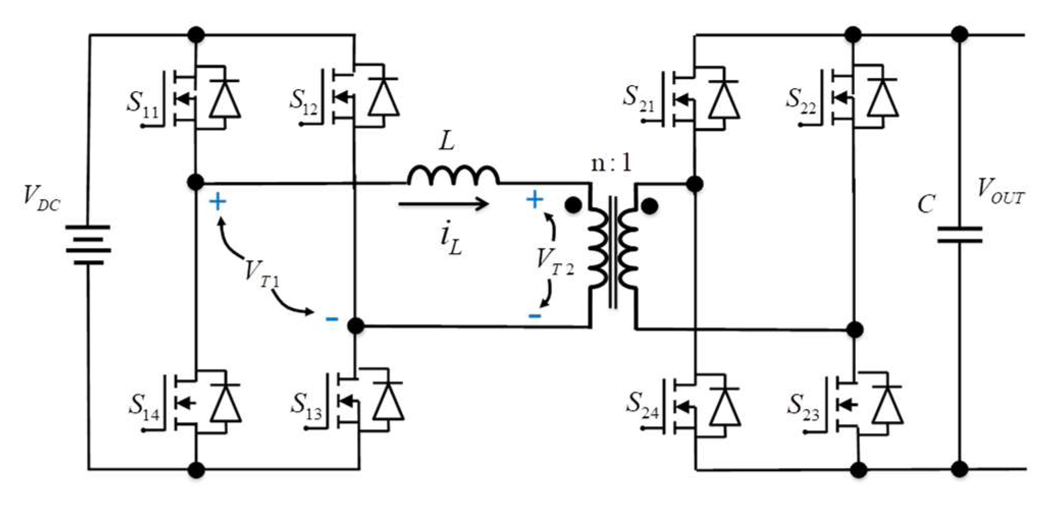
The dual active bridge (DAB) is a dc/dc converter which, due to its flexibility, is employed for different applications, such as solid-state transformers [1,2,3], transportation applications [4,5,6], and renewable energy [7,8]. The converter, shown in Figure 1, comprises two inverters and a high-frequency transformer (HFT). This topology provides isolation between the input and output but also reduces the volume and space. Additionally, the output voltage and power level may be selected by design.
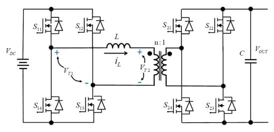
Figure 1.
Dual active bridge (DAB) converter.
The DAB converter is operated traditionally as two dc/ac converters, where its voltage outputs are square or quasi-square waveforms, with a phase shift between them. Depending on the number of displacement angles used, the classification might be as a single-phase-shift (SPS) modulation, which uses only one displacement angle, or multi-phase solutions such as dual-phase-shift (DPS), extended-phase-shift (EPS), or triple-phase-shift (TPS), as shown in [9]. All the previously mentioned modulations should be derived from the TPS, making them special cases when one or two displacement angles remain constant or are equal to each other.
These modulation techniques focus, generally, on reducing losses by implementing different operating modes and increasing the soft-switching power range [10,11,12,13,14,15,16]. In [10], a modulation-based algorithm to control the DAB power flow is proposed; mainly to minimize the total power losses of the DAB converter. A similar method is proposed in [11], which is focused on assuring soft switching in the whole power range, by changing the modulation technique. Different modes of operation are proposed in [12] to increase the efficiency, the burst mode and frequency change are considered. In [13], a proportional value modulation is proposed to reduce the reactive current at different operating points. The double quasi-square output operation is analyzed in [14,15] and proposes a method to reduce the reactive current for losses reduction, resulting in a complex system.
The work in [17] is focused on incorporating soft switching to the DAB converter through a resonant topology. Resonant topologies have the soft switching advantage; however, more components and the resonant tank tuning are drawbacks to consider.
In [18], a cooperative TPS, as it was named, was presented. This modulation allows zero current switchings (ZCS) during an extended power range and low RMS current, at the expense of more complex calculus.
In [19,20], different SPS modulations are presented. However, the modulations analyzed are like the EPS, where two-phase displacement angles are equal, which is a special case of the DPS modulation. In [21,22], the studies of EPS and TPS modulations are shown. To obtain the best efficiency is the main goal of these studies.
The main idea of this work is to study a different scheme, entitled two-stage modulation, that keeps the simple operation. The work also tries to give directions for selecting the most efficient modulation depending on the DAB converter conditions, which consider power factor, RMS current, and soft switching regions. The different modulations are described, analyzed, and experimentally validated.
The paper is organized as follows: in Section 2 the traditional DAB converter operation is discussed, this will permit to derive the different two-stage modulations. In Section 3, one modulation is analyzed in detail, but providing information for the different modulations to be addressed. The experimental results are presented in Section 4. Finally, some conclusions are drawn.
2. Dual Active Bridge Converter
The simplified circuit considered for the DAB converter is shown in Figure 2, where two square or quasi-square voltage sources are considered plus the inductive element [23]. VDC or V1 is the amplitude of the input source (VT1); VOUT is the output voltage, then the second source (VT2) has an amplitude of V2 or nVOUT, where the transformer ratio is n:1.
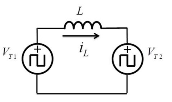
Figure 2.
DAB simplified circuit.
The voltage V2 may be higher or lower than V1, then two operating modes occur [11]. When V2 is higher than V1, the boosting mode happens; but when V2 is lower than V1, the converter operates in bucking mode.
Traditional Single-Phase-Shift Modulation
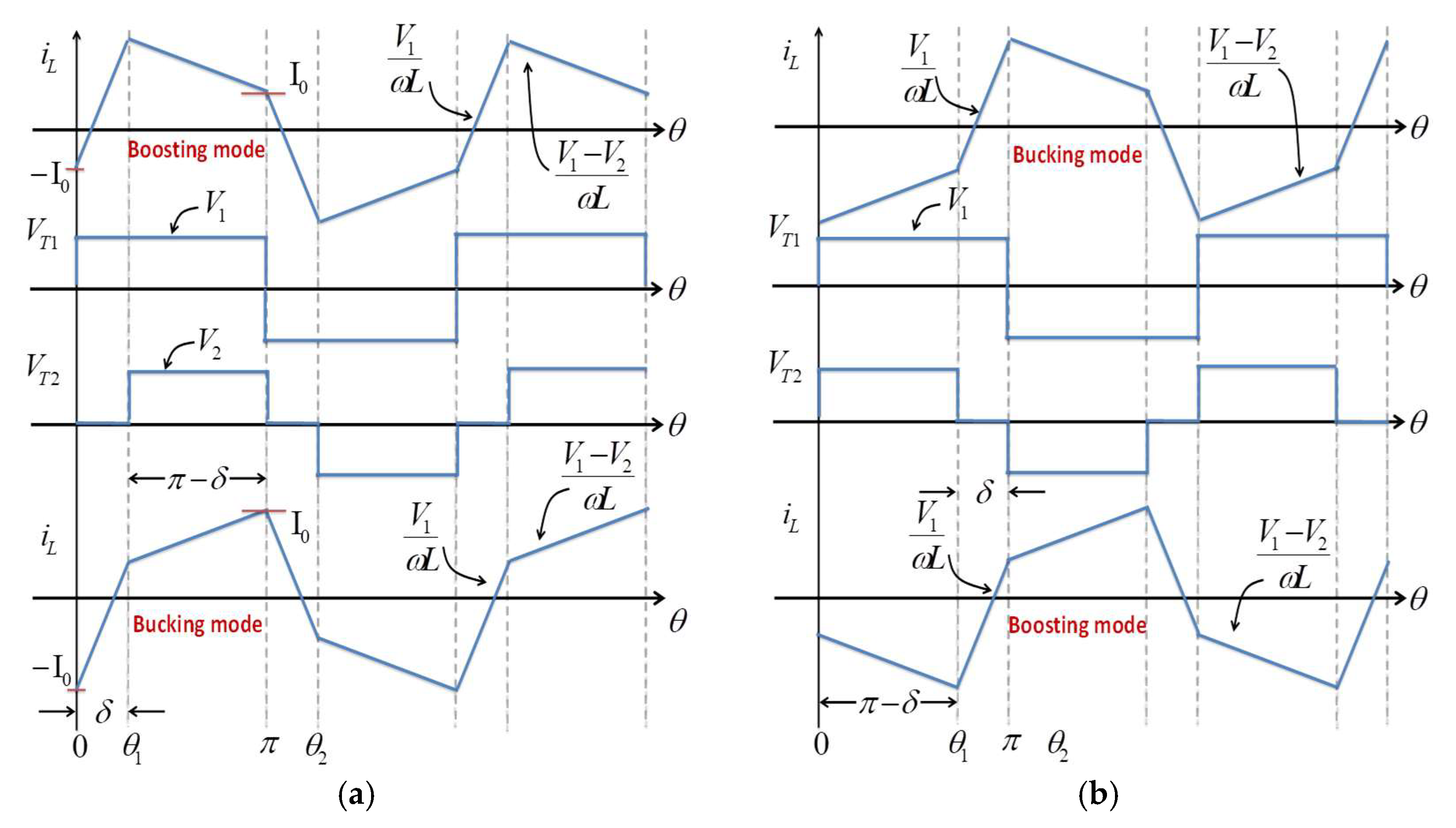
The simplest modulation for a DAB converter is the SPS modulation since only one angle is employed to regulate the output voltage. The typical steady-state waveforms of the DAB converter, for this operation, are shown in Figure 3. The upper current waveform corresponds to the boosting mode operation (V2 > V1), the lower current waveform corresponds to the bucking mode operation (V2 < V1). The whole waveform occurs in four stages, but only two are described due to the symmetry:
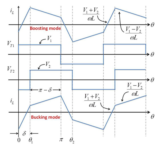
Figure 3.
Traditional single-phase-shift (SPS) modulation main waveforms.
- From 0 < θ < δ. The output of VT1 is positive (VDC), but the output of VT2 is negative (-nVOUT). During this time, the inductor current will increase.
- From δ < θ < π. The output of VT1 is still positive (VDC), but the output of VT2 is now positive (nVOUT) as well. During this time, the inductor current will increase if the bucking mode happens or will decrease if the boosting mode occurs.
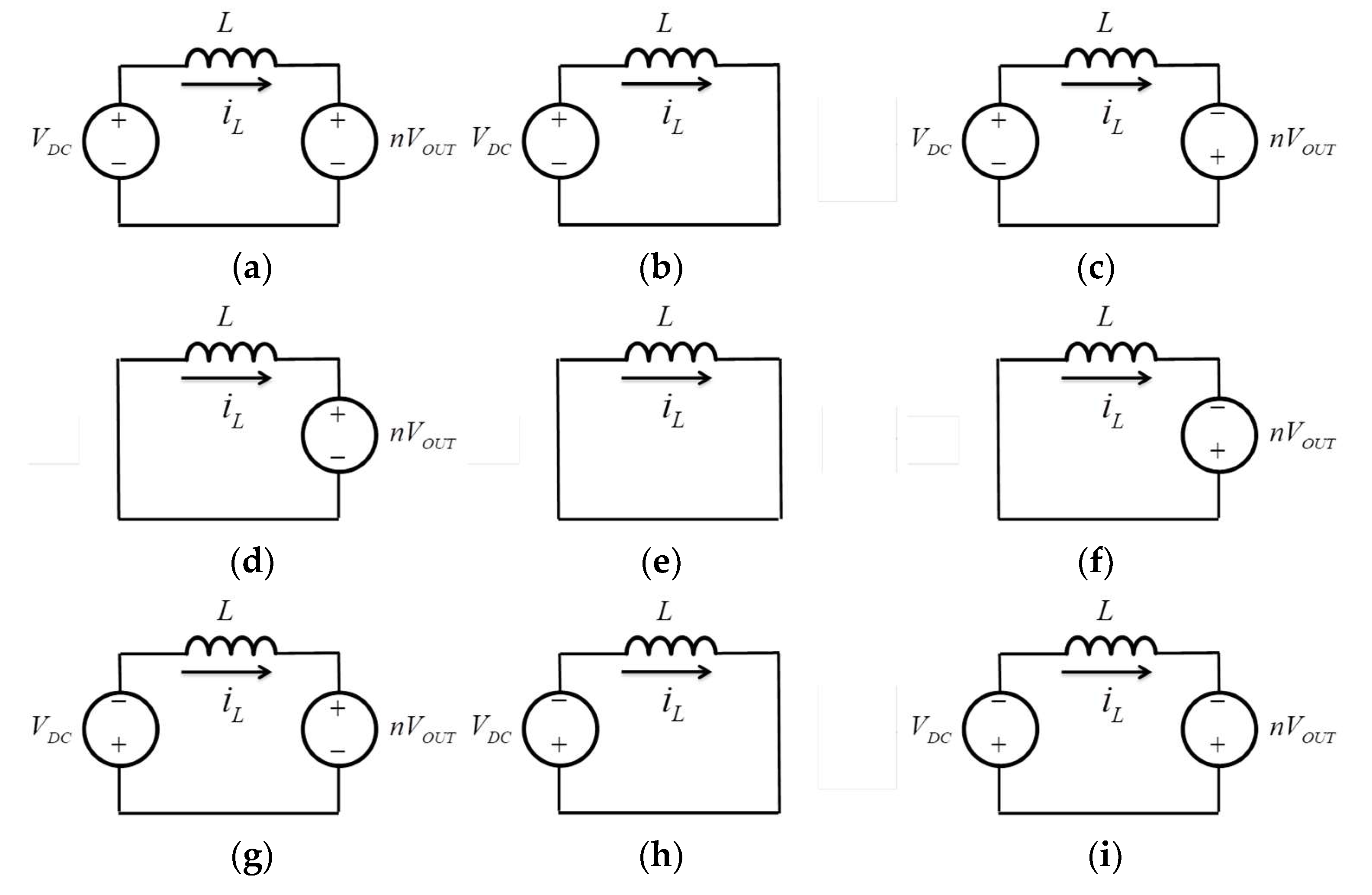
Four different stages are employed for typical modulation. All the possible switching states are shown in Figure 4. As can be observed, the stages “c” and “a” are employed for the positive semi-cycle, and the stages are “g” and “i” for the negative semi-cycle. It can be observed that stages “c” and “g” are equivalent, but for the opposite semi-cycle the same happens for stages “a” and “i”. As shown in Figure 4, there are more than four switching stages and, therefore, other possibilities are open to analysis but, keeping the simplicity, only two switching stages are similar to SPS modulation.

Figure 4.
Different DAB stages, entitled as they are labelled.
3. Two-Stage Modulations
Different switching stages can be employed for the DAB converter (Figure 4). In this work, for the positive semi-cycle (considering the high-frequency transformer voltage), five different switching states are employed to define the complete modulation, since the others are considered equivalent for the negative semi-cycle (Table 1). Therefore, to obtain the complete waveforms it is only necessary to consider one semi-cycle and to use Table 1 for the equivalency and determine the waveforms of the complete period.

Table 1.
Stages equivalency.
The two-stage modulation only employs as the name indicate two switching states for the positive semi-cycle; to assure the power transfer, the positive voltage of both the input and output voltage must be included in at least one of the stages, and to provide good efficiency it is suggested the stage when both are positive (stage “a”) is used.
In Table 2, different two-stage modulations are given. As an example, the stages “b” and “a” are considered for the positive semi-cycle, which define a different modulation; we called this boost modulation since have the best characteristics in boosting mode. To obtain the complete period the stages “h” and “i” are used for the negative semi-cycle since they are the equivalent stages (Table 1). The boost modulation is described in detail in the next sections, but the operation is easily extrapolated to the other two-stage modulations.
Table 2.
Two-stage modulations possible states.
3.1. Boost Modulation
The steady-state waveforms of the boost modulation are shown in Figure 5. It the ac voltage sources with their respective phase displacement can be observed, but also the inductor current is shown. For the direct power transfer, the upper current waveform corresponds to the boosting mode of operation (V2 > V1), the lower current waveform corresponds to the bucking mode of operation (V2 < V1).
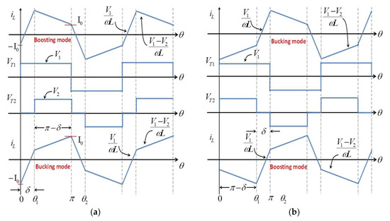
Figure 5.
Boost modulation waveforms: (a) direct power transfer, (b) reverse power transfer.
The full operation occurs in four stages, but only two are described due to the symmetrical behavior (Figure 5a):
- From 0 < θ < δ. The output of VT1 is positive (VDC), but the output of VT2 is zero. During this time, the inductor current will be increased.
- From δ < θ < π. The output of VT1 is again positive (VDC), but the output of VT2 is now positive (nVOUT). During this time, the inductor current will be increased if the bucking mode happens or will be decreased if the boosting mode occurs.
Similarly, then, the aforementioned occurs at the switching period. It can be observed that stages “b” and “h” are equivalent, but one for the positive, and the other for the negative semi-cycle. The same happens for “a” and “i”.
3.2. Bidirectional Power
Another characteristic of the DAB converter is the power bidirectionality, which is considered in different applications. All the two-stage modulations can also be operated for reversal power transfer, waveforms for boost modulation are shown in Figure 5b; now, the angle δ, is measured since π/2, not from 0 degrees. The difference with direct power transfer is that the switching states are now appearing in inverse order.
The full operation occurs in four stages again, but only two are described due to the symmetry:
- From 0 < θ < δ. The output of VT1 and VT2 are both positive (VDC and nVOUT). During this time, the inductor current will be increased if the bucking mode happens or will be decreased if the boosting mode occurs.
- From δ < θ < π. The output of VT1 is positive (VDC), but the output of VT2 is now zero. During this time, the inductor current will be increased.
As can be observed, the current has a polarity change, and then the power flows oppositely. As with the positive transfer, the angle δ can only take values between 0 and π/2.
3.3. Steady-State Analysis
The boost modulation is analyzed in this section. For this, Figure 5a is considered, then the inductor current may be expressed as:
where: ω is the angular switching frequency,
I0 is the initial current,
L is the inductance of the topology.
The other semi-cycle of the inductor current is omitted since it is symmetrical, due to the ac operation. Note that the vertical axis was shifted to determine the second equation, and this was done for simplification purposes in the analysis.
The value of the inductor current at π − δ is determined by:
Then, the initial current value may be determined from (2), and it is given by:
The active power can be determined by considering just the first semi-cycle, that is:
Then considering the intervals of the current, Equation (4) becomes:
Considering (1), (3), (5), and simplifying is obtained:
It can be noticed that (6) is half of the typical equation considered for traditional SPS modulation.
The RMS value of the inductor current is determined by:
Solving (7) is obtained by:
The apparent power referred to the input voltage (V1) is determined by:
The power factor (PF) for the input voltage is then:
Table 3 summarizes the equations for the modulations under study.
Table 3.
Two-stage modulation equations.
3.4. Soft-Switching
The DAB converter may operate at soft-switching depending on the operating conditions. Each branch of the two bridges may have a different condition. For the boost modulation, both input bridge branches have the next condition:
But the output bridge branches have the following two conditions:
Condition (12) is for the left branch and (13) for the right branch. Notice that (11) and (12) are exactly opposite conditions, then the soft-switching operation cannot be guaranteed for all the branches at the same time.
The soft switching occurs only when a small capacitor is placed in parallel with the MOSFET (drain-source), otherwise, all the devices will be operating at hard switching. In order to calculate the capacitor value, the following formula may be used:
where: CZVS is the capacitor value,
Imin is the minimum inductor current at each transition;
td is the blanking time; and
VCZVS is the capacitor voltage.
For the boost modulation, the best operation is when three branches can operate at soft-switching conditions, then a small capacitor should be added to respective branches.
Table 4 shows the conditions for all the modulations studied. As can be derived from Table 4, the traditional SPS may operate all the branches at soft switching at the same time; the boost and buck modulations only three branches at the same time; and finally the flyback modulation only two branches may operate at soft switching at the same time.
Table 4.
Soft switching conditions.
3.5. Discussion on Two-Stage Modulation
Different graphs were obtained for the different two-stage modulations to evaluate its performance under different conditions, and this is based on the previous analysis which considers the equations in Table 3.
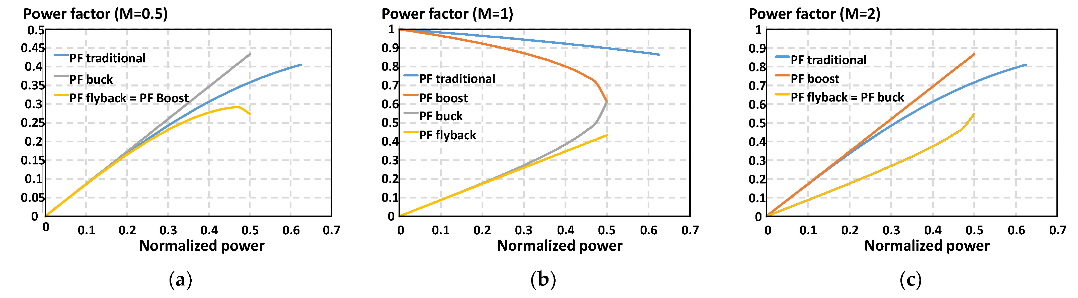
Figure 6 shows the PF of the different modulations at different gains (M = V2/V1), gains 0.5, 1, and 2 were selected, a power normalization was made considering the maximum power of the traditional SPS modulation. For just the traditional modulation, the power can reach the maximum power, but for the others, only half of the power can be reached in correspondence with the theory (Table 3). As can be observed in Figure 6a, for M = 0.5, the buck modulation offers the best PF, and this modulation is suggested for M < 0.55. For M = 1, the traditional SPS modulation offers the best power PF (Figure 6b) and, indeed, this is the best PF that can be achieved for all cases. For M = 2, the boost modulation has the best PF (Figure 6c), and this technique is suggested for M > 1.45. The higher the PF, the fewer conduction losses that are expected and, therefore, the higher the efficiency.
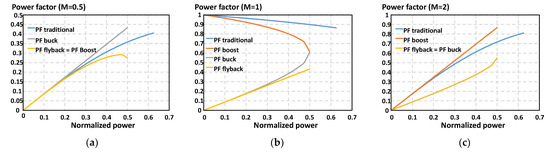
Figure 6.
Power factor referred to the input voltage: (a) M = 0.5, (b) M = 1, and (c) M = 2.
Depending on the applications and consequently the operating conditions, the best two-stage modulation should be selected according to the designed M. Since the best PF possible is obtained with a gain M = 1, the converter should be worked in this condition, when possible, and using the traditional SPS modulation.
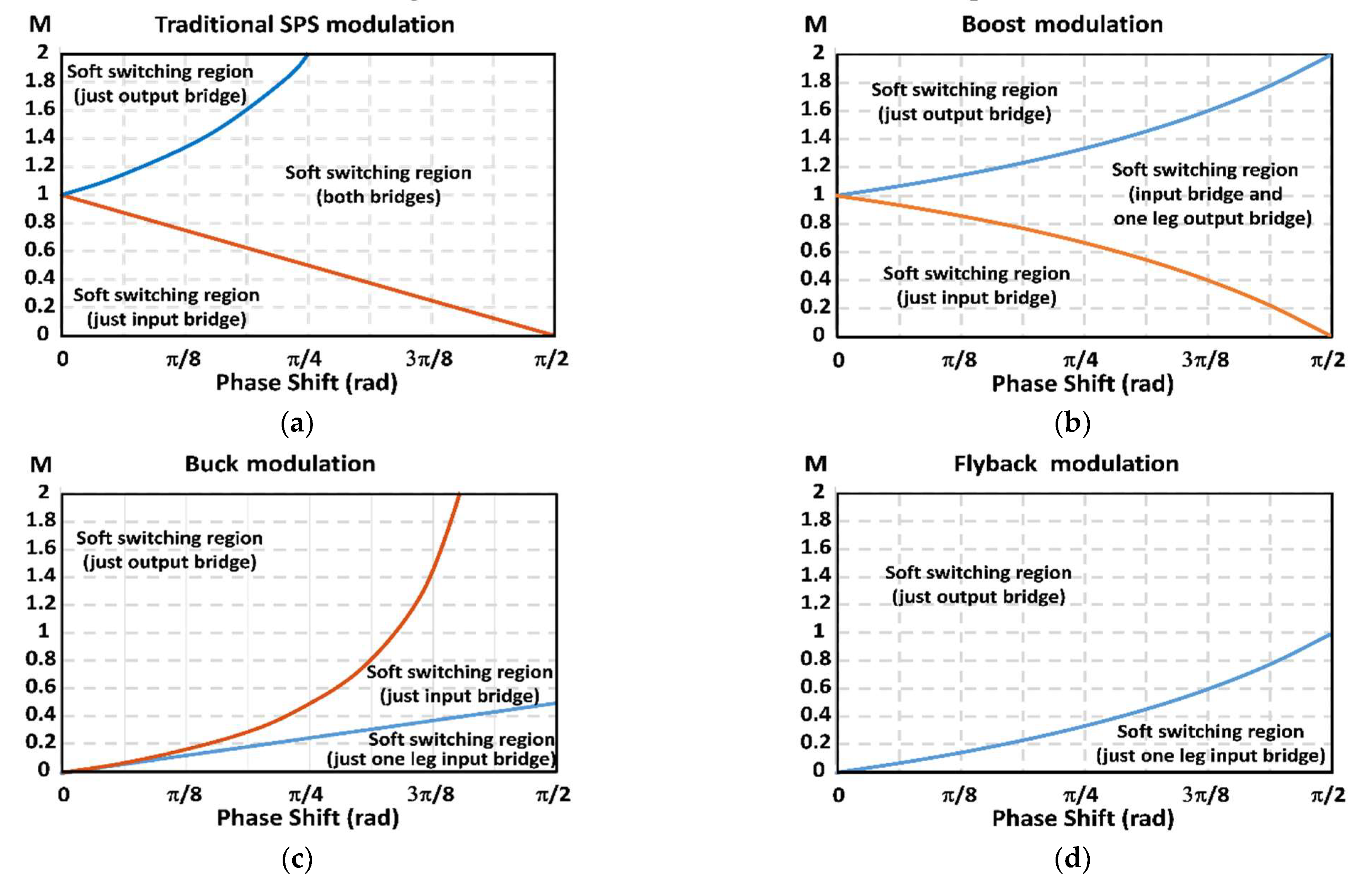
On the other hand, Figure 7 shows the regions where soft switching can be obtained. In Figure 7a can be observed the soft-switching region for the traditional SPS; Figure 7b shows the soft switching region for the boost modulation; while in Figure 7c the region where the buck modulation has soft switching is illustrated; finally, Figure 7d depicts the soft switching area for the flyback modulation. Each modulation has its best operating region. It is observable that the soft switching is dependent on the respective displacement angle and the voltage gain (M). However, some modulations are not viable for achieving soft switching in all its devices, as was explained in Section 3.4.
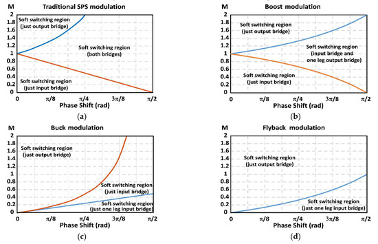
Figure 7.
Soft switching regions: (a) traditional SPS modulation, (b) boost modulation, (c) buck modulation, and (d) flyback modulation.
For the traditional SPS, the best region to operate is near M = 1 for both PF and soft-switching conditions; for the boost modulation it is M > 1 for soft switching conditions and also the best PF; the best conditions for the buck modulation are M < 0.6 for PF, and low angles for soft switching conditions; the flyback modulation has the worst PF in all cases, and the worst soft-switching scenario.
Efficiency depends on two factors: conduction losses and switching losses. The first one is related to the PF and the second can be eliminated if the soft-switching conditions are satisfied. The best two-stage modulation should be selected depending on the operating conditions but considering the PF and the soft switching region.
4. Experimental Results
A power converter was designed and experimentally tested. The parameters are summarized in Table 5. To evaluate the performance of the system, different tests were carried out. The performance of each operating condition was evaluated, and the efficiency and the RMS current of the inductor were measured. All the tests were carried out in hard-switching conditions.
Table 5.
Experimental test parameters.
4.1. Steady-State Waveforms
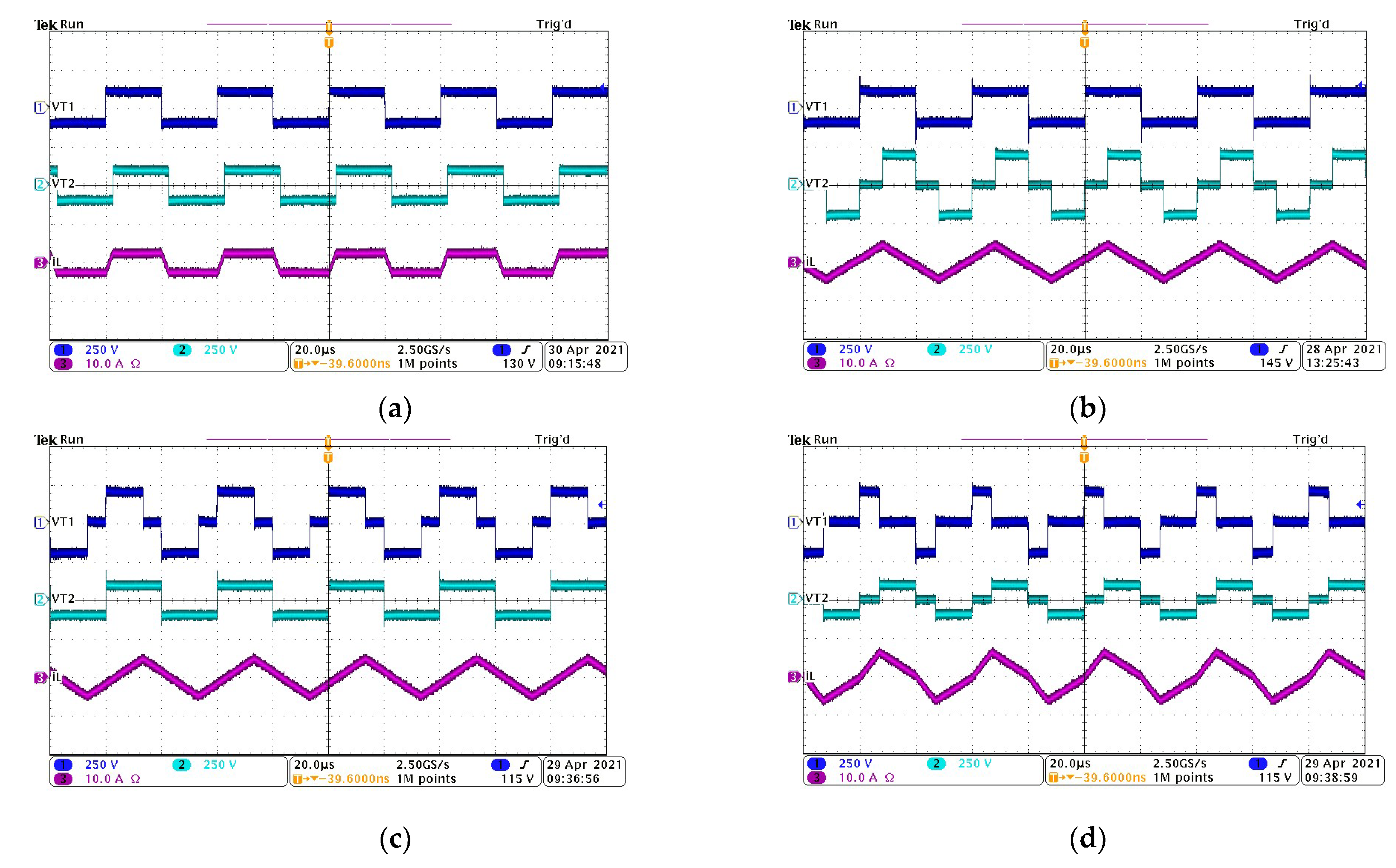
Figure 8 shows the waveforms for the different two-stage modulations. The ac voltage sources with their respective phase displacement can be observed, but also the inductor current is shown. In Figure 8a the traditional SPS modulation is shown when M = 1. In Figure 8b, the boost modulation occurs when the DAB operates in boosting mode (M = 2). Figure 8c,d show the DAB waveforms (M = 0.5) for the buck and flyback modulations, respectively. As can be observed, the waveforms correspond with the described operation and effectively two stages are employed to define the DAB operation.
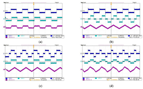
Figure 8.
Experimental results. From top to bottom, input bridge output voltage, output bridge reflected output voltage, transformer inductance current: (a) traditional SPS modulation, for M = 1, (b) boost modulation, for M = 2, (c) buck modulation, for M = 0.5, and (d) flyback modulation, for M = 0.5.
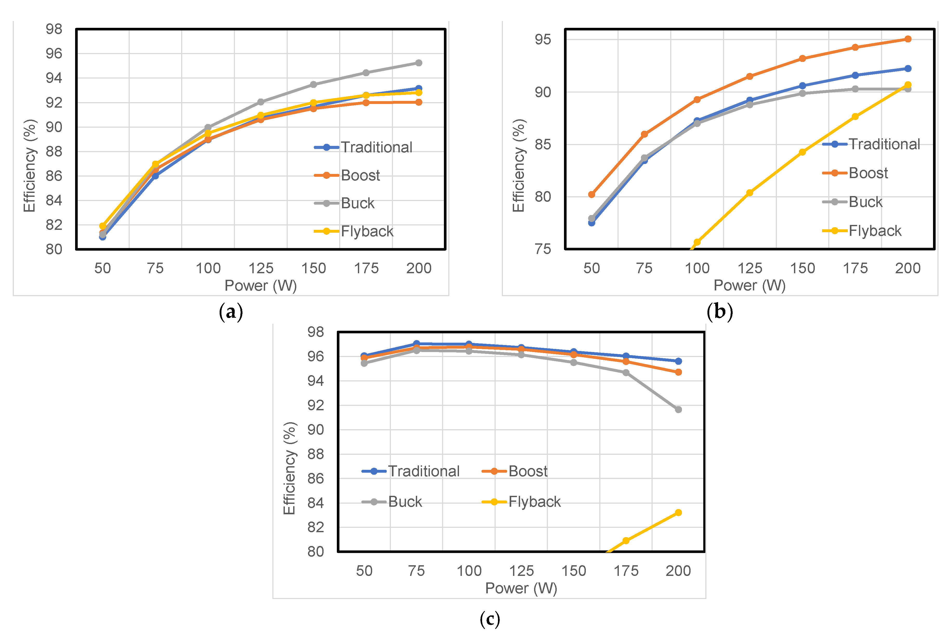
4.2. Efficiency
Figure 9 shows the efficiency for the different two-stage modulations. Figure 9a illustrates the efficiency operating in boosting mode, while in Figure 9b the bucking mode efficiency might be observed; and, in Figure 9c, the efficiency when M = 1 is depicted. It can be observed that traditional SPS have better efficiency when M = 1, as is expected due to the behavior described in the power factor section. However, better performance is observed for the boost and buck modulations when the converter operates in the bosting or bucking mode, respectively. This is the boost modulation that is better for M = 2, and the buck modulation is best for M = 0.5.
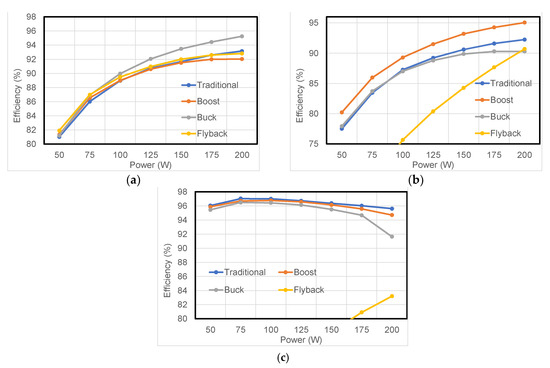
Figure 9.
Efficiency results for: (a) M = 0.5, (b) M = 1, (c) M = 2.
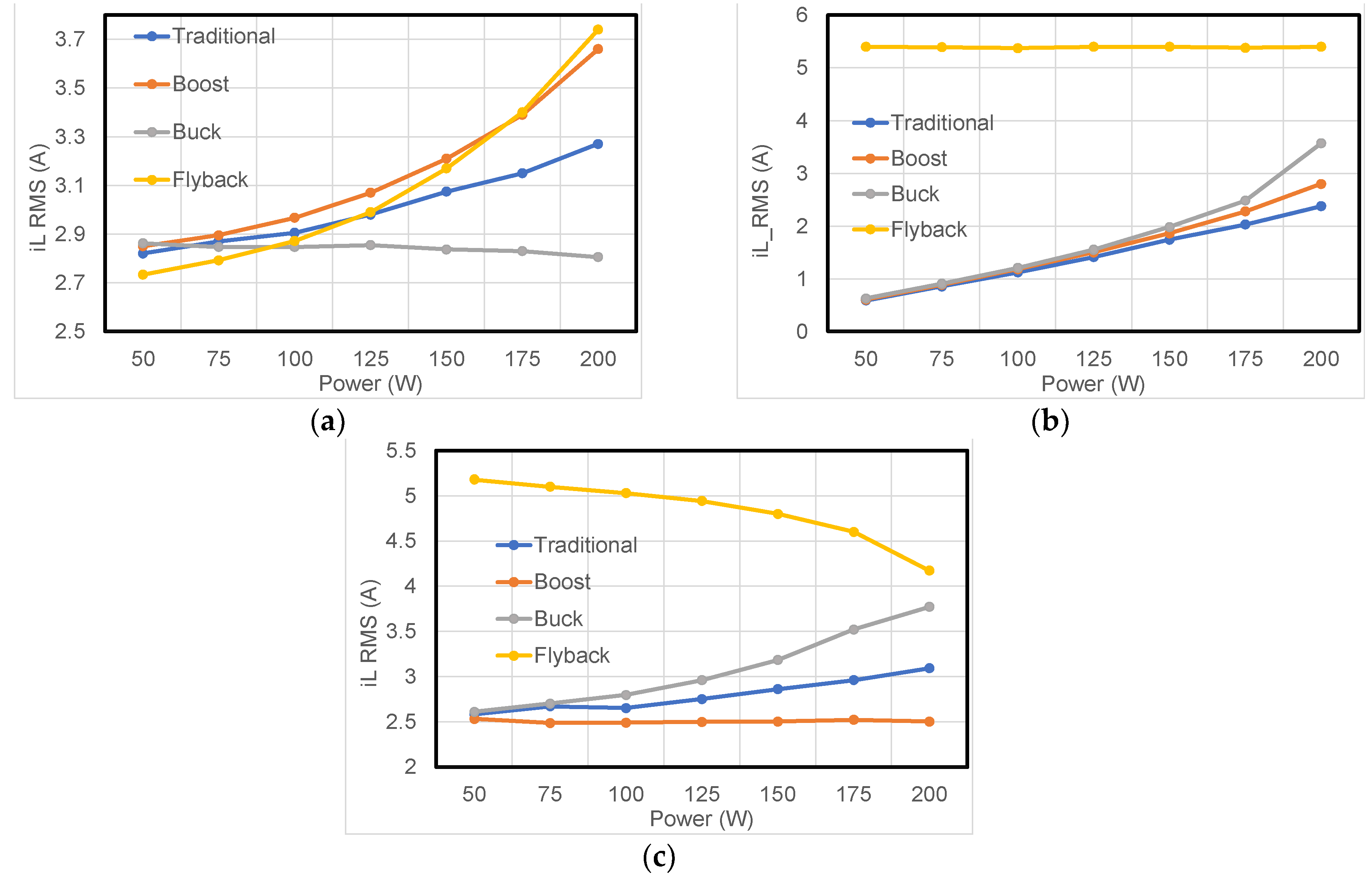
4.3. RMS Inductor Current
The inductor RMS currents are shown in Figure 10 and, as can be observed, each two-stage modulation has an optimal operating region. Figure 10a corresponds to M = 0.5, Figure 10b to M = 1, and Figure 10c to M = 2. Again, it can be seen that the traditional SPS has better performance when M = 1; the boost modulation is better for M = 2; and the buck modulation is best for M = 0.5, because of the values of the RMS current.

Figure 10.
Series inductor RMS current for: (a) M = 0.5, (b) M = 1, (c) M = 2.
5. Conclusions
The DAB converter is a widely used converter due to its design flexibility. Single-phase shift is the simplest modulation technique used for the converter. In this paper, different two-stage modulations based on the SPS were analyzed where only two stages are needed to transfer power. The best modulation technique may be selected depending on the operating conditions based on the gain, but considering the PF and the soft switching region since the different modulation offers better performance than the others depending on the operating conditions. Traditional SPS is suggested when gain near one is employed, but when boosting or bucking modes are used, the boost or the buck modulation may be a better option. One of the advantages of the studied modulations is the simplicity of the modulation; only one displacement angle is in fact needed.
The buck modulation operates best when the converter works in bucking mode, while the boost modulation shows better performance when the converter is driven in boosting mode. To validate the analysis, experimental results were conducted, which illustrated the performance of each modulation.
Author Contributions
Conceptualization, P.G., N.V. and M.L.; Formal analysis, P.G.; Funding acquisition, S.E.P.C. and C.H.; Methodology, R.O. and C.H.; Validation, P.G.; Writing—review and editing, N.V., M.L. and S.E.P.C. All authors have read and agreed to the published version of the manuscript.
Funding
This work was supported in part by the Tecnológico Nacional de México under Grant 10722.21-P and by SENACYT under Grant ITE17-R2-006.
Conflicts of Interest
The authors declare no conflict of interest.
References
- Das, D.; Hrishikesan, V.M.; Kumar, C.; Liserre, M. Smart Transformer-Enabled Meshed Hybrid Distribution Grid. IEEE Trans. Ind. Electron. 2020, 68, 282–292. [Google Scholar] [CrossRef]
- Ruiz, F.; Perez, M.A.; Espinosa, J.R.; Gajowik, T.; Stynski, S.; Malinowski, M. Surveying Solid-State Transformer Structures and Controls: Providing Highly Efficient and Controllable Power Flow in Distribution Grids. IEEE Ind. Electron. Mag. 2020, 14, 56–70. [Google Scholar] [CrossRef]
- Liserre, M.; Buticchi, G.; Andresen, M.; De Carne, G.; Costa, L.; Zou, Z.-X. The Smart Transformer: Impact on the Electric Grid and Technology Challenges. IEEE Ind. Electron. Mag. 2016, 10, 46–58. [Google Scholar] [CrossRef] [Green Version]
- Buticchi, G.; Costa, L.F.; Barater, D.; Liserre, M.; Amarillo, E.D. A Quadruple Active Bridge Converter for the Storage Integration on the More Electric Aircraft. IEEE Trans. Power Electron. 2017, 33, 8174–8186. [Google Scholar] [CrossRef] [Green Version]
- Krismer, F.; Kolar, J.W. Accurate power loss model derivation of a high-current dual active bridge converter for an auto-motive application. IEEE Trans. Ind. Electron. 2010, 57, 881–891. [Google Scholar] [CrossRef]
- Naayagi, R.; Shuttleworth, R.; Forsyth, A. Bidirectional control of a dual active bridge DC–DC converter for aerospace applications. IET Power Electron. 2012, 5, 1104–1118. [Google Scholar] [CrossRef]
- Shi, Y.; Li, R.; Xue, Y.; Li, H. Optimized Operation of Current-Fed Dual Active Bridge DC–DC Converter for PV Applications. IEEE Trans. Ind. Electron. 2015, 62, 6986–6995. [Google Scholar] [CrossRef]
- Zhu, R.; de Carne, G.; Deng, F.; Liserre, M. Integration of large photovoltaic and wind system by means of smart trans-former. IEEE Trans. Ind. Electron. 2017, 64, 8928–8938. [Google Scholar] [CrossRef] [Green Version]
- Hou, N.; Li, Y.W. Overview and Comparison of Modulation and Control Strategies for a Nonresonant Single-Phase Dual-Active-Bridge DC–DC Converter. IEEE Trans. Power Electron. 2019, 35, 3148–3172. [Google Scholar] [CrossRef]
- Oggier, G.G.; García, G.O.; Oliva, A.R. Switching Control Strategy to Minimize Dual Active Bridge Converter Losses. IEEE Trans. Power Electron. 2009, 24, 1826–1838. [Google Scholar] [CrossRef]
- Oggier, G.G.; García, G.; Oliva, A.R. Modulation strategy to operate the dual active bridge DC–DC converter under soft switching in the whole operating range. IEEE Trans. Power Electron. 2010, 26, 1228–1236. [Google Scholar] [CrossRef]
- Oggier, G.G.; Ordonez, M. High-Efficiency DAB Converter Using Switching Sequences and Burst Mode. IEEE Trans. Power Electron. 2015, 31, 2069–2082. [Google Scholar] [CrossRef]
- Rodriguez-Rodrıguez, J.R.; Moreno-Goytia, E.L.; Venegas-Rebollar, V.; Ugalde-Caballero, L.E.; Anaya-Ruiz, G.A. The Pro-portional-Values Modulation (PVM), a technique for improving efficiency and power density of bidirectional DAB converters. Electr. Power Syst. Res. 2017, 144, 280–289. [Google Scholar] [CrossRef]
- Shi, H.; Wen, H.; Chen, J.; Hu, Y.; Jiang, L.; Chen, G. Minimum-Reactive-Power Scheme of Dual-Active-Bridge DC–DC Converter with Three-Level Modulated Phase-Shift Control. IEEE Trans. Ind. Appl. 2017, 53, 5573–5586. [Google Scholar] [CrossRef] [Green Version]
- Hou, N.; Song, W.; Li, Y.W.; Zhu, Y.; Zhu, Y. A Comprehensive Optimization Control of Dual-Active-Bridge DC–DC Converters Based on Unified-Phase-Shift and Power-Balancing Scheme. IEEE Trans. Power Electron. 2018, 34, 826–839. [Google Scholar] [CrossRef]
- Byen, B.J.; Ban, C.H.; Lim, Y.B.; Choe, G.H. An Efficiency-Optimized Modulation Strategy for Dual-Active-Bridge DC–DC Converters Using Dual-Pulse-Width-Modulation in the Low Power Region. J. Power Electron. 2017, 17, 1413–1421. [Google Scholar]
- Yaqoob, M.; Loo, K.-H.; Lai, Y.M. Fully Soft-Switched Dual-Active-Bridge Series-Resonant Converter with Switched-Impedance-Based Power Control. IEEE Trans. Power Electron. 2018, 33, 9267–9281. [Google Scholar] [CrossRef]
- Wu, F.; Feng, F.; Gooi, H.B. Cooperative Triple-Phase-Shift Control for Isolated DAB DC–DC Converter to Improve Current Characteristics. IEEE Trans. Ind. Electron. 2019, 66, 7022–7031. [Google Scholar] [CrossRef]
- Mou, D.; Luo, Q.; Li, J.; Wei, Y.; Chen, J. The Novel Single Phase-Shift Modulation Scheme for Dual Active Bridge Converter. Proceedings of 2020 IEEE 9th International Power Electronics and Motion Control Conference (IPEMC2020-ECCE Asia), Nanjing, China, 29 November–2 December 2020; pp. 2686–2690. [Google Scholar] [CrossRef]
- An, F.; Song, W.S.; Yang, K.X. Optimized power control with extended phase shift in dual-active-bridge dc–dc converters. Electron. Lett. 2018, 54, 651–653. [Google Scholar] [CrossRef]
- Zhao, B.; Yu, Q.; Sun, W. Extended-Phase-Shift Control of Isolated Bidirectional DC–DC Converter for Power Distribution in Microgrid. IEEE Trans. Power Electron. 2012, 27, 4667–4680. [Google Scholar] [CrossRef]
- Gu, Q.; Yuan, L.; Nie, J.; Sun, J.; Zhao, Z. Current Stress Minimization of Dual-Active-Bridge DC–DC Converter Within the Whole Operating Range. IEEE J. Emerg. Sel. Top. Power Electron. 2018, 7, 129–142. [Google Scholar] [CrossRef]
- Dutta, S.; Hazra, S.; Bhattacharya, S. A Digital Predictive Current-Mode Controller for a Single-Phase High-Frequency Transformer-Isolated Dual-Active Bridge DC-to-DC Converter. IEEE Trans. Ind. Electron. 2016, 63, 5943–5952. [Google Scholar] [CrossRef]


Publisher’s Note: MDPI stays neutral with regard to jurisdictional claims in published maps and institutional affiliations. |
© 2021 by the authors. Licensee MDPI, Basel, Switzerland. This article is an open access article distributed under the terms and conditions of the Creative Commons Attribution (CC BY) license (https://creativecommons.org/licenses/by/4.0/).