Article

Conception and Simulation of a 2-Then-1-Bit/Cycle Noise-Shaping SAR ADC

1
Department of Electrical and Electronic Engineering, Konkuk University, Seoul 05029, Korea
2
Department of Electrical Engineering, Korea Advanced Institute of Science and Technology (KAIST), Daejeon 34141, Korea
*
Author to whom correspondence should be addressed.
Electronics 2021, 10(20), 2545; https://doi.org/10.3390/electronics10202545
Submission received: 2 September 2021 / Revised: 15 October 2021 / Accepted: 16 October 2021 / Published: 18 October 2021
(This article belongs to the Section Circuit and Signal Processing)

Abstract

:
A 2-then-1-bit/cycle noise-shaping successive-approximation register (SAR) analog-to-digital converter (ADC) for high sampling rate and high resolution is presented. The conversion consists of two phases of a coarse 2-bit/cycle SAR conversion for high speed and a fine 1-bit/cycle noise-shaping SAR conversion for high accuracy. The coarse conversion is performed by both voltage and time comparison for low power consumption. A redundancy after the coarse conversion corrects the error caused by a jitter noise during the time comparison. Additionally, a mismatch error between signal and reference paths is eliminated with the help of a tail-current-sharing comparator. The proposed ADC was designed in a 28 nm CMOS process, and the simulation result shows a 68.2 dB signal-to-noise distortion (SNDR) for a sampling rate of 480 MS/s and a bandwidth of 60 MHz with good energy efficiency.

Graphical Abstract

1. Introduction

A successive approximation register (SAR) analog-to-digital converter (ADC) is well-known to have high energy efficiency for medium bandwidth and moderate resolution. When the SAR ADC needs to achieve high resolution, however, the comparator power and the size of a capacitive digital-to-analog converter (CDAC) increase exponentially, and the energy efficiency would decrease significantly. In addition, a conventional SAR algorithm that requires at least N comparisons to obtain N-bit results limits the maximum sampling rate. Therefore, SAR ADCs are not optimal for applications that require both high resolution and high speed. To overcome those limitations while maintaining high energy efficiency of SAR ADCs, hybrid ADCs that combine SAR and other ADCs have been developed in recent years.
A multi-bit/cycle SAR ADC is a hybrid one that boosts conversion speed by utilizing a flash ADC in a SAR ADC [1,2]. It reduces the total number of comparisons by converting more than two bits per comparison cycle. Regardless of the high sampling rate, the resolution of a multi-bit/cycle SAR ADC is still limited by the same comparator requirement. A noise-shaping SAR ADC is another kind of SAR-based hybrid ADC, and it performs oversampling and noise-shaping similar to a ΔΣ ADC [3]. It can provide quite high resolution with very good energy efficiency; however, its bandwidth is often limited by oversampling and filter latency.
This article presents a 2-then-1-bit/cycle noise-shaping SAR ADC that utilizes two aforementioned hybrid ADCs for its coarse conversion and fine conversion, respectively, to take only their advantages. The proposed ADC performs fast coarse 2-bit/cycle SAR conversion and then does fine 1-bit/cycle SAR conversion with noise-shaping capability for high resolution. This approach can mitigate the trade-off between resolution and speed, as in Figure 1, which shows the achievable bandwidth of SAR-based ADCs versus signal-to-noise and distortion ratio (SNDR). Therefore, the proposed ADC can achieve high resolution as well as high sampling rate compared with conventional SAR-based ADCs.
The rest of this article is organized as follows. In Section 2, the proposed ADC architecture is described. The circuit implementation is presented in Section 3, and transistor-level simulation results are discussed in Section 4. Finally, Section 5 concludes this article.

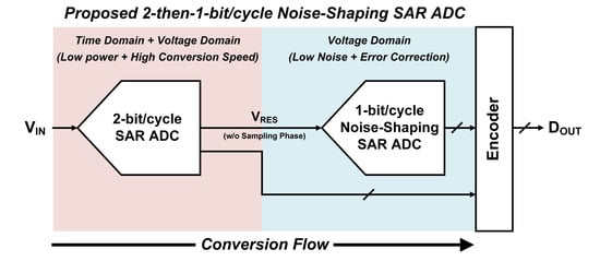
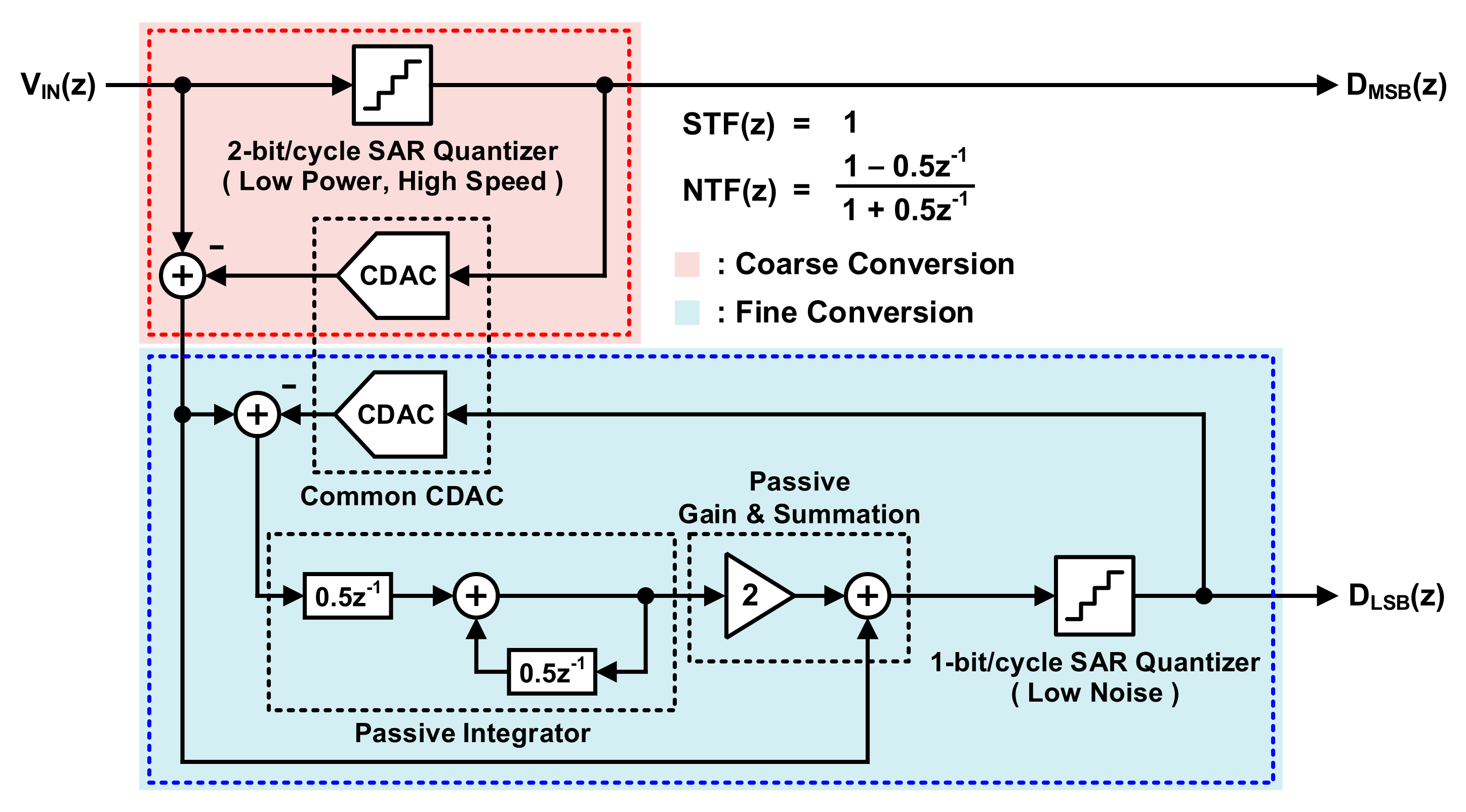
2. Proposed 2-then-1-bit/cycle Noise-Shaping SAR ADC Architecture

The proposed 2-then-1-bit/cycle noise-shaping SAR ADC performs fast and coarse 2-bit/cycle SAR conversion first. Then, it is followed by a fine conversion, which is a first-order noise-shaping SAR conversion based on 1-bit/cycle for accuracy, as shown in Figure 2. The fine conversion includes redundancy at the beginning to correct the error in the coarse conversion. The coarse and fine conversion can be accomplished on the same CDAC, as will be explained in Section 3, so each conversion can be optimized maximally without causing any mismatch issue or performance degradation.

2.1. Coarse SAR Conversion

Figure 3a shows the architecture of a 2-bit/cycle SAR ADC [5] that is used for the coarse SAR conversion of the proposed ADC. There are two voltage comparators and one time comparator based on an SR latch to avoid the use of a multi-input comparator, which is often adopted for multi-bit/cycle conversion [2] but which suffers severely from thermal noise and kick-back noise.
Figure 3b,c shows how the coarse 2-bit/cycle SAR conversion operates. Each conversion cycle involves quantization in the voltage domain and a subsequent quantization in the time domain to generate a 2-bit output. First, the upper output code (D [1]) is generated by comparing Vsigp and Vsign, which represents the top-plate voltage of the signal CDAC that is connected to the input of the comparator, as shown in Figure 3b. At the same time, Vrefp and Vrefn, which provide reference voltage levels for 2-bit comparison and scale down by 1/4 per conversion, are compared, even though the comparison result itself does not affect the output codes. Then, the time comparator compares the two decision times, Tsig and Tref, spent on the two voltage comparators, as in Figure 3c. This time comparison reveals which of the signal and the reference has a larger magnitude, providing the information for the lower output code (D [0]). The time comparison only requires the operation of an SR latch, so the 2-bit conversion can be completed in a similar amount of time as the conventional 1-bit/cycle conversion. Therefore, the required number of conversion cycles can be reduced to improve the overall sampling rate without affecting the energy efficiency much. Additionally, the circuit can be simplified due to the use of the SR latch.
However, the time jitter noise significantly affects the time comparison accuracy and can limit the resolution. To address this issue, a prior work [5] lowers the supply voltage to make jitter noise negligible, although the conversion speed slows down significantly. In contrast, not to sacrifice the conversion speed for lower jitter noise, we adopt the conversion scheme shown in Figure 3a only for most significant bits (MSBs). Any error due to jitter noise during the MSB conversion can be corrected with the following redundant conversion, and the remaining least significant bits (LSBs) are generated from 1-bit/cycle SAR conversion that is free from the jitter noise.

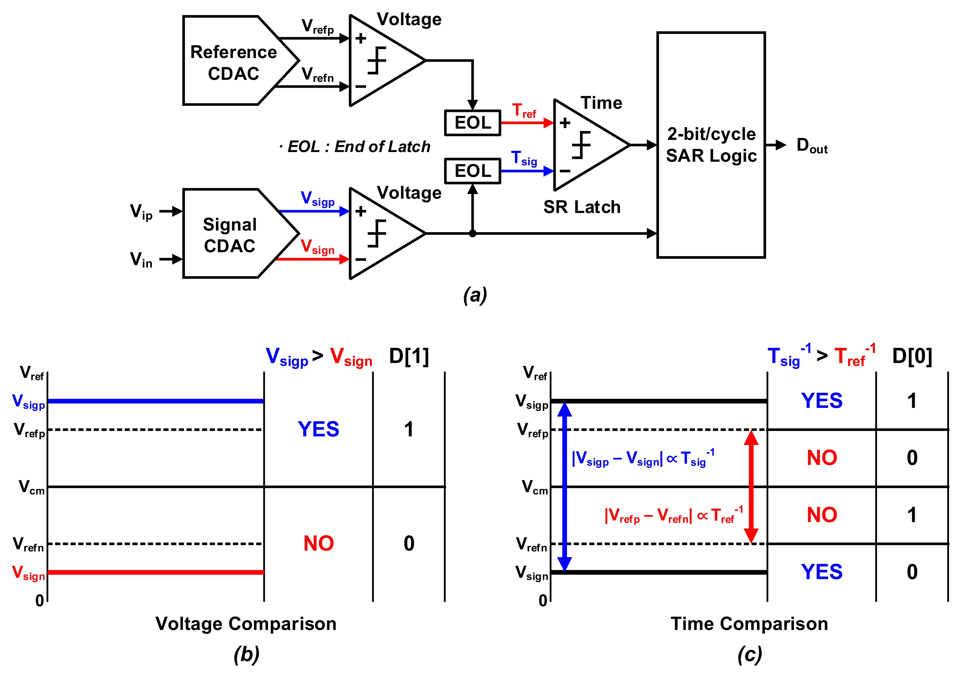
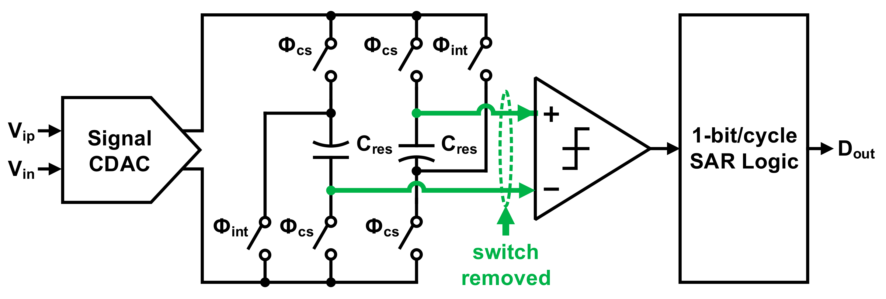
2.2. Jitter Error Correction with Redundancy

Figure 4 shows the conversion process for m-MSBs and n-LSBs to demonstrate how the jitter error can be corrected with redundancy. Noise-shaping is omitted for simplicity. A decision error might occur during MSB [m-3 : m-2] conversion since the residue signal is within the uncertain range where the time comparison can be inaccurate due to the jitter noise. The error from the MSB conversion would affect the result of subsequent LSB conversions if not corrected. By adding redundancy at the beginning of the LSB conversion, the decision error can be easily corrected as the settling error in a conventional SAR ADC. Tolerance to jitter noise due to the redundancy allows faster MSB conversion without compromising the total power consumption or the ADC accuracy. However, the redundant bit size, which is related to the maximum allowable jitter noise, cannot be too large since it will eventually require more conversion cycles for the LSB conversion. The choice of the redundant bit and its relationship to jitter noise are discussed further in Section 3.

2.3. Fine SAR Conversion

The residue signal after the coarse SAR conversion is then converted to LSBs by 1-bit per cycle, for which a separate low-noise voltage comparator is used. The first conversion is for the redundancy, and the fine conversion adopts noise-shaping for higher resolution. Even without noise-shaping during the coarse conversion, the whole ADC can show a noise transfer function (NTF) that is same as that of the fine conversion if the midway update method based on redundancy [6] is used. Therefore, a loop filter is necessary only for the fine conversion and passive integration in [7], provided that the first-order NTF of (1) is adopted to enable noise-shaping without the use of a power-hungry amplifier or a multi-input comparator.
NTF z = 1 0.5 z 1 1 + 0.5 z 1
The passive integrator shown in Figure 5 is based on switched capacitors (SCs). The residue integration capacitor (Cres) is connected to a CDAC, either in parallel for charge sharing during residue integration or in reverse series for passive summation during conversion. Due to the separate MSB and LSB conversions, and hence the use of separate comparators, the top plate of Cres can remain connected to the LSB comparator input, unlike in [7]. Therefore, the switch between Cres and the comparator that causes a severe distortion can be removed and the hardware can be simplified.

3. Circuit Implementation

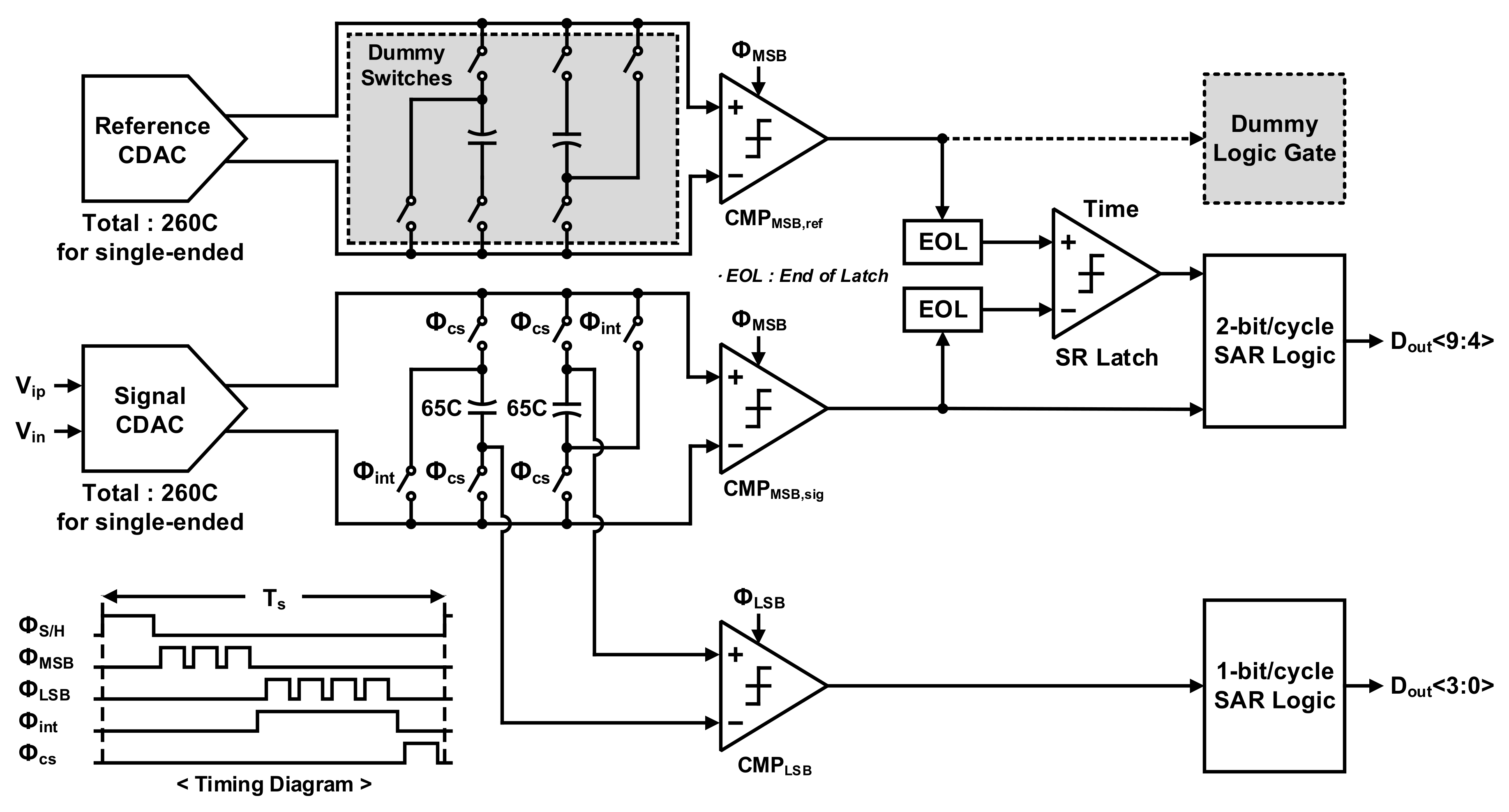
3.1. 2-then-1-bit/cycle Noise-Shaping SAR ADC

Figure 6 shows the top-level circuit implementation of the proposed ADC with total 9-bit conversions. The 3-cycles for 6-bits are assigned to the MSB conversion for the maximum speed of the ADC, which is shown in the timing diagram. In the proposed ADC, the relationship between bit depth and speed is determined by the number of coarse conversion bits and fine conversion bits. Criteria for dividing coarse conversion and fine conversion are set in consideration of the amount of redundancy required to recover the error caused by jitter. As shown in [5], the error caused by jitter is determined by the difference in comparator input voltage, and the smaller the difference, the smaller the error caused by jitter. Whatever the target resolution is, the first comparison always compares the sampled signal with 1/4Vref and 3/4Vref, and thus the same jitter error occurs. Therefore, the required amount of redundancy is independent of the number of bits, so increasing the number of coarse conversion bits is effective in terms of conversion speed.
Two CDACs for signal and reference, two dynamic voltage comparators (CMPMSB,sig, CMPMSB,ref), and an SR latch time comparator are used for the MSB conversion. The two voltage comparators are optimized only for speed and low power consumption since their noise performance is not important. The signal CDAC is also used for 4-bit LSB conversion, together with a fully passive SC integrator connected to it. Due to the use of the same signal CDAC, the LSB conversion can start immediately, with the residue signal remaining on the CDAC after the MSB conversion without an additional sampling phase, as in a pipelined structure [8,9]. Additionally, there is no gain error that might occur from the use of different CDACs. A separate SAR logic as well as a separate comparator (CMPLSB) designed for low noise are used for the LSB conversion.
In addition to core blocks for operation, dummy switches and logics are added to the reference CDAC and comparator, respectively, to balance the signal and reference paths. A mismatch between the two paths might cause signal-independent time delay that leads to a large time comparator offset. Moreover, the CDACs would have different gain and kick-back noise from the comparators without dummy blocks, affecting the linearity of MSBs significantly. The effect by mismatch could be severe depending on process, voltage, and temperature (PVT) variations, so the dummy blocks are essential for suppressing any routing and parasitic mismatch.

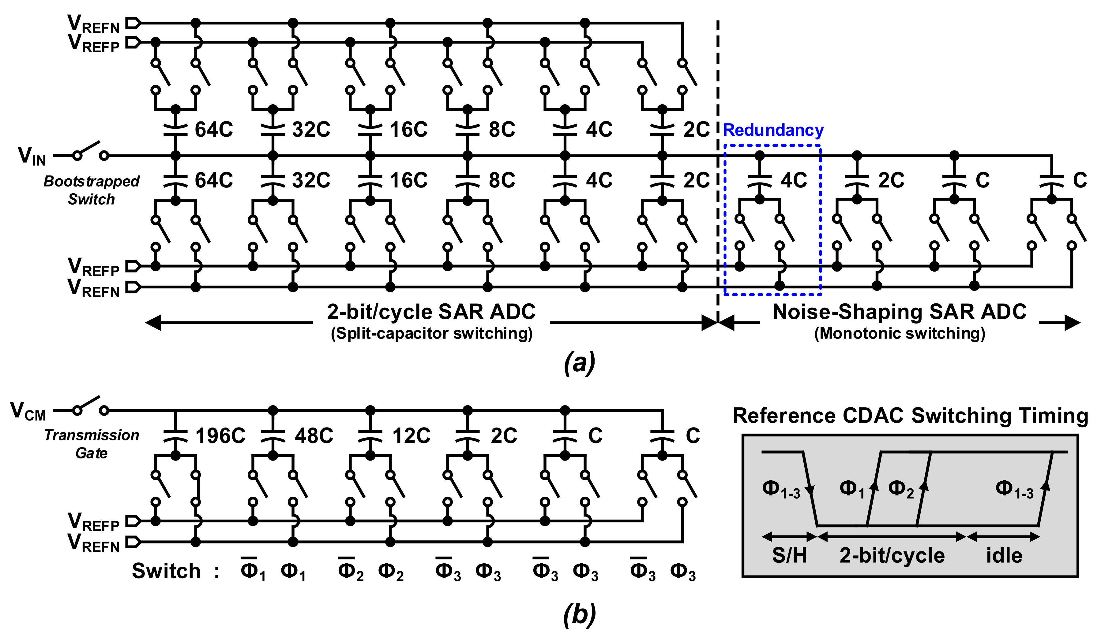
3.2. Signal CDAC and Reference CDAC

As mentioned above, matching between the signal and reference CDACs is critical. Therefore, the signal and reference CDACs are made of the same unit capacitor and have an equal number of unit capacitors (260C), minimizing the unbalanced kick-back noise and gain mismatch to ensure high conversion accuracy.
For the signal CDAC, two kinds of switching methods are used in combination so that the switching energy is optimized for each conversion, as shown in Figure 7a. During the 6-bit MSB conversion, the common-mode voltage of the signal and reference CDACs should be the same for accurate time comparison. The common-mode voltage difference acts as an offset for the time comparator. Therefore, a split-capacitor switching [10] maintaining the common-mode voltage to Vcm is used during the MSB conversion. On the other hand, the LSB conversion requires only one voltage comparator, so it is immune to the common-mode voltage variation. A monotonic switching [11] is employed to reduce switching power and to simplify the switching logic. The reference CDAC is also switched monotonically during the MSB conversion, and then it remains idle, as shown in Figure 7b.

3.3. Redundant Bit Size

Figure 8 shows the uncertain range for each cycle during 6-bit MSB conversion. Our simulation shows that the time difference Tdiff (= Tsig − Tref) is proportional to the magnitude difference of signal and reference in LSBs (Vdiff) of Equation (2), as shown in Figure 8.
V diff = V sigp   -   V sign   -   V refp   -   V refn V LSB  
The uncertain range is confined by the region where jitter noise is larger than |Tdiff|. Both the slope of voltage-to-time conversion and the jitter noise increase as the conversion progresses since the reference voltage gets smaller. However, since the slope increases faster, the uncertain range becomes narrower in subsequent conversion cycles. Therefore, the first MSB conversion cycle shows the widest uncertain range that determines the redundant bit size. From the result shown in Figure 8, a redundant bit of at least 4 LSB size is necessary to correct the error from the worst-case jitter noise. To ensure the performance of the proposed ADC against PVT variations, comparator offset and mismatch between signal and reference paths caused by charge injection, clock feedthrough, and parasitic component, etc., an 8 LSB size redundant bit (=4C) is added for some margin.

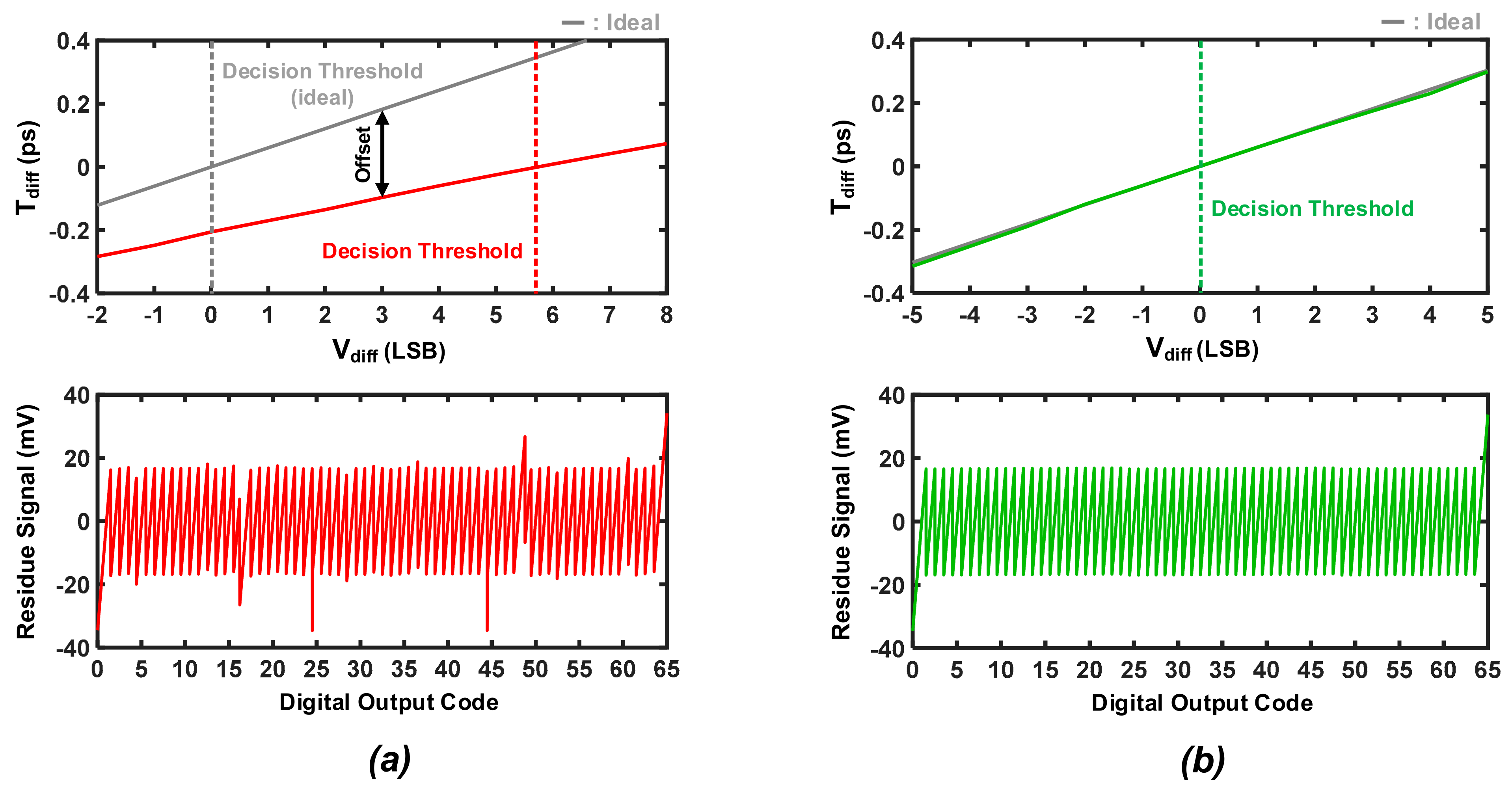
3.4. Proposed Tail-Current-Sharing Comparator

The decision time of a comparator [12] should be determined only by the input signal voltage for the accuracy during MSB conversion, so the signal and reference paths are designed to be geometrically identical to avoid any mismatch, as mentioned previously. However, there are signal-dependent parameters for transistors that become a dynamic mismatch between the two paths and cause a decision error. Especially, the trans-conductance of input transistors in the comparators (gm,input) shown in Figure 9a varies due to the input signal and affects the decision time substantially. The tail node voltages of the two comparators (CMPMSB,sig, CMPMSB,ref), VX and VY in Figure 9a, are set differently by the input signal and reference voltages during sampling phase due to parasitic capacitances of Cp,input and Cp,tail, as in Figure 9b. Therefore, there exists a time-varying offset between the two comparators having different gm,input due to VX and VY. Figure 10a shows the offset and the resulting residue signal with errors that are quite large and difficult to be corrected by redundancy.
To mitigate it, VX and VY could be reset to a fixed voltage during the sampling phase, but it requires additional switches as well as a non-overlapping clock that slow down the speed and increase hardware complexity. Instead, we short the tail nodes so that the two comparators always have the same gm,input for the differential input pairs during the conversion, as shown in Figure 9. The proposed tail-current-sharing comparator with the common tail node voltage of VZ does not show any signal-dependent offset and can provide an error-free residue signal for the fine conversion, as in Figure 10b. Therefore, the offset can be eliminated simply by shorting the two nodes, without any overhead in hardware size, power consumption, and speed. In addition, the signal part and the reference part share the same supply voltage, which means that they will have the same power supply rejection ratio (PSRR) and that there is no performance degradation from it.

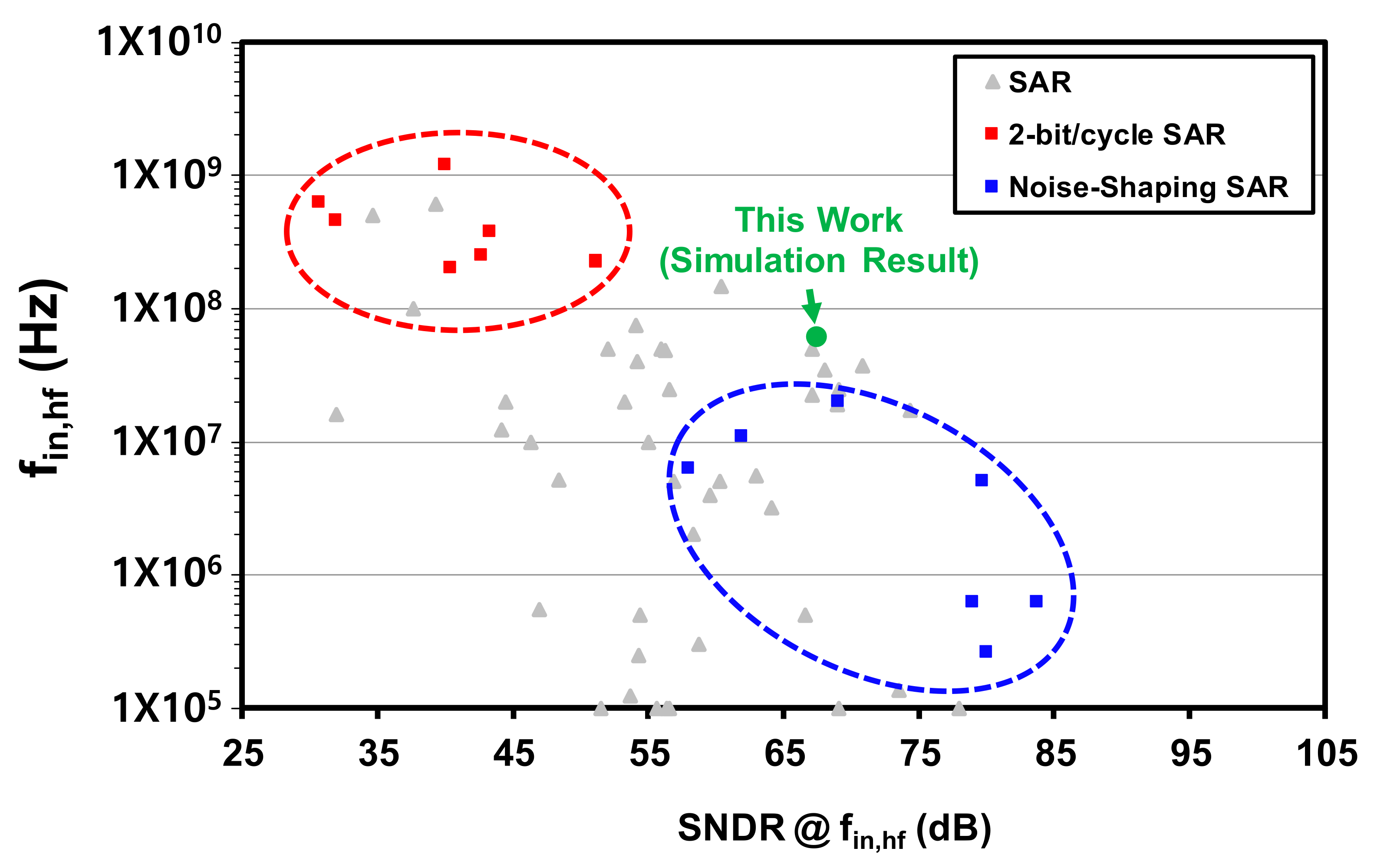
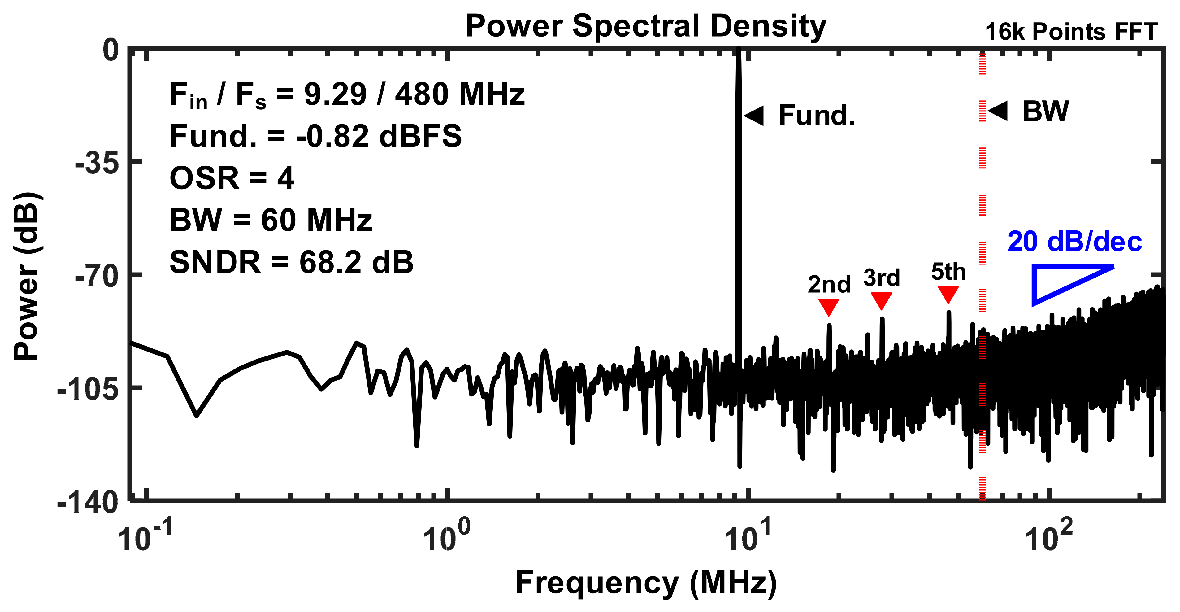
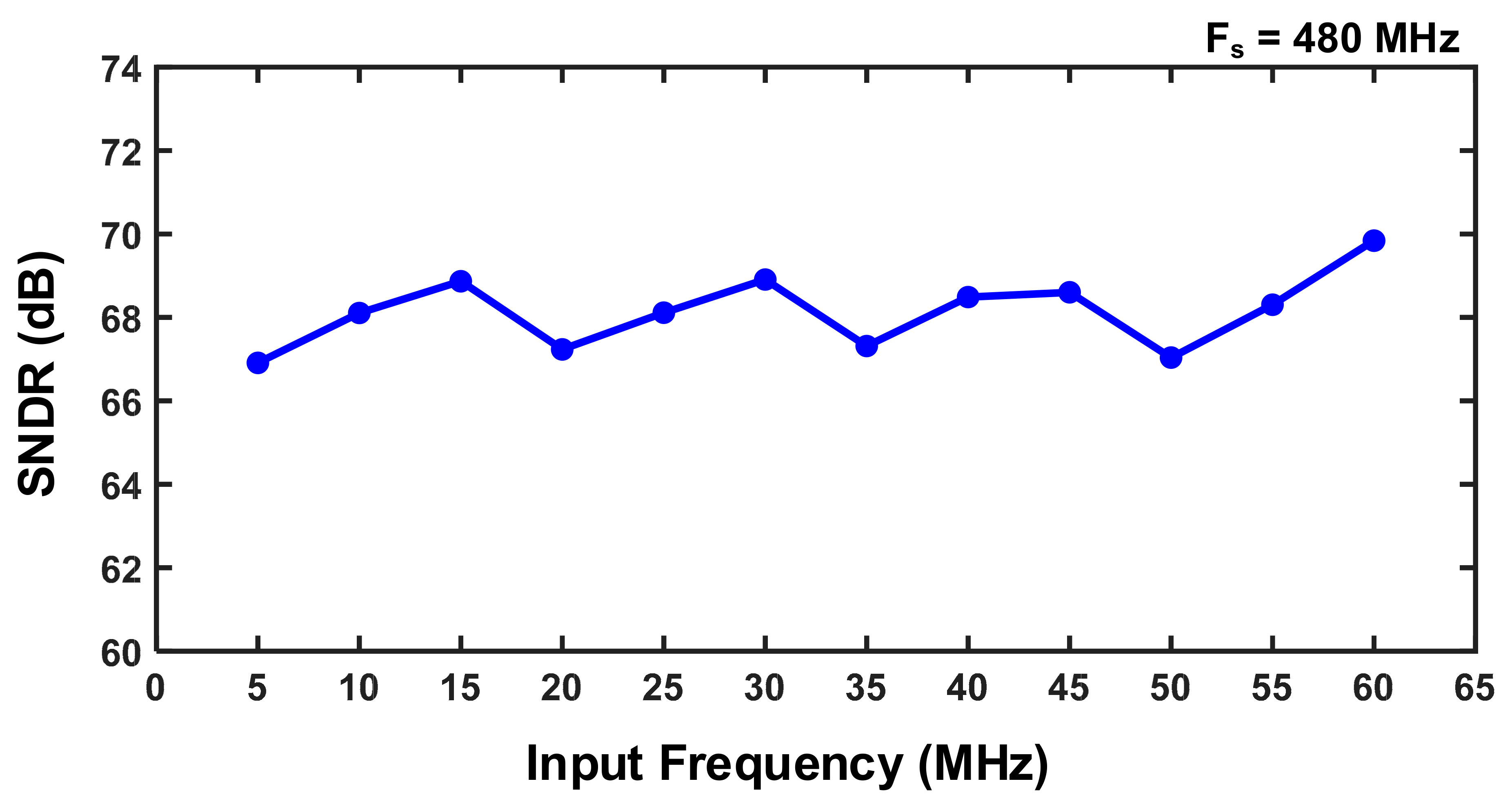
4. Simulation Results

The proposed 2-then-1-bit/cycle noise-shaping SAR ADC is designed fully at a transistor level in a 28 nm CMOS process. All simulations were performed with only the transistor level parasitic capacitance and resistance, which was information based on the P-Cell layout regression provided by the foundry to reduce the error between post-layout simulation and pre-layout simulation. In addition, transient noise up to 100 GHz, 1% mismatch for the CDAC with 1.2-fF unit capacitors, which was a value that allowed CDAC to contain systematic mismatch and random mismatch of less than 1% and to have kT/C noise of 13.259 nV2, as well as the comparator offset were included. Figure 11 shows the histograms of coarse signal comparator, coarse reference comparator, and fine comparator offset voltage based on the Monte Carlo simulation. The proposed ADC was designed to have an offset calibration circuit [13], which has 5 mV and 1 mV resolutions, so the coarse and fine comparators operate with offsets less than 5 mV and 1 mV, respectively.
Figure 12 shows the output power spectral density of the proposed ADC with a sampling rate of 480 MS/s. An input signal at 9.29 MHz with a magnitude of −0.82 dBFS was used. The result shows an SNDR of 68.2 dB for a 60 MHz bandwidth (OSR = 4). The total power consumption of the proposed ADC was 2.13 mW under a 1.1 V supply voltage. Figure 13 shows the simulated SNDR versus the input frequency at 480 MS/s. A flat result was obtained from 5 MHz to 60 MHz. Figure 14 shows the SNDR variation according to the temperature from −40 °C to 140 °C under different process corners. Simulations for each corner were performed at sampling rates of SS: 430 MHz, TT: 480 MHz, and FF: 540 MHz, respectively, and it can be seen that almost the same SNDR was obtained at all temperatures.
Table 1 shows the performance summary of the proposed ADC and compares it with prior works. The 2-then-1-bit/cycle noise-shaping SAR ADC achieved higher SNDR than a 2-bit/cycle SAR ADC with a similar power consumption. However, there can be a significant difference between actual measurement and simulation results. Therefore, a simulation result from a 1-bit/cycle noise-shaping SAR ADC was also added for better comparison. The bandwidth of the proposed ADC can be increased by 33% while not affecting the accuracy or energy efficiency.

5. Conclusions

This brief presents a 2-then-1-bit/cycle noise-shaping SAR ADC that achieves both high sampling rate and high resolution. The coarse 2-bit/cycle SAR conversion enhances the sampling rate by reducing the number of conversion cycles. A proposed tail-current-sharing comparator was used to minimize the error during the coarse conversion due to mismatch. Additionally, a 1-bit redundancy was added to correct the error caused by jitter noise. The fine 1-bit/cycle SAR conversion improved the resolution with the help of the first-order noise-shaping that was implemented passively. Therefore, the proposed ADC is not only scaling-friendly but also helpful for improving both sampling rate and resolution with a good energy efficiency and without using any amplifier or a multi-input comparator.

Author Contributions

Conceptualization, K.K. and H.C.; methodology, K.K. and S.O.; software, K.K.; validation, K.K.; formal analysis, K.K.; investigation, K.K. and S.O.; resources, H.C.; data curation, K.K.; writing—original draft preparation, K.K.; writing—review and editing, K.K. and H.C.; visualization, K.K.; supervision, K.K. and H.C.; project administration, H.C.; funding acquisition, H.C. All authors have read and agreed to the published version of the manuscript.

Funding

This research was supported by the Samsung Science & Technology Foundation (SRFC-IT1092-C4).

Conflicts of Interest

The authors declare no conflict of interest.

References

  1. Cao, Z.; Yan, S.; Li, Y. A 32 mW 1.25 GS/s 6b 2b/Step SAR ADC in 0.13 μm CMOS. IEEE J. Solid-State Circuits 2009, 44, 862–873. [Google Scholar] [CrossRef]
  2. Hong, H.; Kim, W.; Park, S.; Choi, M.; Park, H.; Ryu, S. A 7b 1GS/s 7.2 mW nonbinary 2b/cycle SAR ADC with register-to-DAC direct control. In Proceedings of the IEEE Custom Integrated Circuits Conference, San Jose, CA, USA, 9–12 September 2012. [Google Scholar]
  3. Frendenburg, J.; Flynn, M. A 90-MS/s 11-MHz-bandwidth 62-dB SNDR noise-shaping SAR ADC. IEEE J. Solid State Circuits 2012, 47, 2898–2904. [Google Scholar] [CrossRef]
  4. ADC Performance Survey 1997–2021. Available online: https://web.stanford.edu/~murmann/adcsurvey.html (accessed on 2 September 2021).
  5. Luo, J.; Liu, Y.; Li, J.; Ning, N.; Wu, K.; Liu, Z.; Yu, Q. A Low Voltage and Low Power 10-bit Non-Binary 2b/Cycle Time and Voltage Based SAR. IEEE Trans. Circuits Syst. I Regular. Pap. 2020, 67, 1136–1148. [Google Scholar] [CrossRef]
  6. Jie, L.; Zheng, B.; Flynn, M. 20.3 A 50MHz-Bandwidth 70.4dB-SNDR Calibration-Free Time-Interleaved 4th-Order Noise-Shaping SAR ADC. In Proceedings of the IEEE International Solid-State Circuits Conference, San Francisco, CA, USA, 17–21 February 2019. [Google Scholar]
  7. Lin, Y.; Lin, C.; Tsai, S.; Lu, C. 20.2 A 40MHz-BW 320MS/s passive Noise-Shaping SAR ADC with Passive Signal-Residue Summation in 14nm FinFET. In Proceedings of the IEEE International Solid-State Circuits Conference, San Francisco, CA, USA, 17–21 February 2019. [Google Scholar]
  8. Song, Y.; Chan, C.-H.; Zhu, Y.; Martins, R.P. A 12.5-MHz Bandwidth 77-dB SNDR SAR-Assisted Noise Shaping Pipeline ADC. IEEE J. Solid-State Circuits 2020, 55, 312–321. [Google Scholar] [CrossRef]
  9. Hsu, C.-K.; Tang, X.; Liu, J.; Xu, R.; Zhao, W.; Mukherjee, A.; Andeen, T.R.; Sun, N. A 77.1-dB-SNDR 6.25-MHz-BW Pipeline SAR ADC with Enhanced Interstage Gain Error Shaping and Quantization Noise Shaping. IEEE J. Solid-State Circuits 2021, 56, 739–749. [Google Scholar] [CrossRef]
  10. Ginsburg, B.; Chandrakasan, A. 500-MS/s 5-bit ADC in 65-nm CMOS with Split Capacitor Array DAC. IEEE J. Solid-State Circuits 2007, 42, 739–747. [Google Scholar] [CrossRef]
  11. Sanyal, A.; Sun, N. An Energy-Efficient Low Frequency-Dependence Switching Technique for SAR ADCs. IEEE Trans. Circuits Syst. II Express Briefs 2014, 65, 294–298. [Google Scholar]
  12. Babayan-M, S.; Lotfi, R. Analysis and design of a low-voltage low-power double-tail comparator. IEEE Trans. Very Large Scale Integr. Syst. 2014, 22, 343–352. [Google Scholar] [CrossRef]
  13. Miitteregger, G.; Ebner, C.; Mechnig, S.; Blon, T.; Holuigue, C.; Romani, E. A 20-mW 640-MHz CMOS Continuous-Time ΔΣ ADC with 20-MHz Signal Bandwidth, 80-dB Dynamic Range and 12-bit ENOB. IEEE J. Solid-State Circuits 2012, 41, 2641–2649. [Google Scholar] [CrossRef]
  14. Chan, C.; Zhu, Y.; Sin, S.U.; Martins, R.P. A 3.8mW 8b 1GS/s 2b/cycle interleaving SAR ADC with compact DAC structure. In Proceedings of the Symposium on VLSI Circuits Digest of Technical Papers, Honolulu, HI, USA, 13–15 June 2012. [Google Scholar]
  15. Lin, Y.; Tsai, C.; Tsou, S.; Chu, R.; Lu, C. A 2.4-mW 25-MHz BW 300-MS/s Passive Noise Shaping SAR ADC with Noise Quantizer Technique in 14-nm CMOS. In Proceedings of the Symposium on VLSI Circuits, Kyoto, Japan, 5–8 June 2017. [Google Scholar]
  16. Tsai, T.-H.; Tai, H.-Y.; Tsai, P.-Y.; Tsai, C.-H.; Chen, H.-S. An 8 b 700 MS/s 1 b/cycle SAR ADC using a delay-shift technique. IEEE Trans. Circuits Syst. I Regular. Pap. 2016, 63, 683–692. [Google Scholar] [CrossRef]
  17. Song, J.; Park, Y.; Lim, C.; Choi, Y.; Ahn, S.; Park, S.; Kim, C. A 9-bit 500-MS/s 2-bit/cycle SAR ADC with Error-Tolerant Interpolation Technique. IEEE J. Solid-State Circuits 2021. [Google Scholar] [CrossRef]
Figure 1. Bandwidth versus resolution of SAR-based ADCs [4] and simulation result of proposed ADC.
Electronics 10 02545 g001
Figure 2. Block diagram of proposed 2-then-1-bit/cycle noise-shaping SAR ADC.
Electronics 10 02545 g002
Figure 3. (a) Architecture of 2-bit/cycle SAR ADC for coarse conversion: (b) voltage comparison for upper bit; (c) time comparison for lower bit.
Electronics 10 02545 g003
Figure 4. Conversion process for m-bit MSBs and n-bit LSBs and jitter error correction with redundancy.
Electronics 10 02545 g004
Figure 5. First-order noise-shaping SAR ADC architecture for fine conversion.
Electronics 10 02545 g005
Figure 6. Top-level implementation of proposed ADC.
Electronics 10 02545 g006
Figure 7. Schematic of (a) signal CDAC and (b) reference CDAC.
Electronics 10 02545 g007
Figure 8. Simulated decision time difference versus normalized voltage difference and uncertain range.
Electronics 10 02545 g008
Figure 9. (a) Proposed tail-current-sharing comparator and (b) transient of tail node voltages.
Electronics 10 02545 g009
Figure 10. Simulated time comparator offset and residue signal after coarse conversion: (a) conventional; (b) proposed.
Electronics 10 02545 g010
Figure 11. Histograms of the (a) coarse signal comparator, (b) coarse reference comparator, and (c) fine comparator offset voltage from Monte Carlo simulations with 1000 cases.
Electronics 10 02545 g011
Figure 12. Simulated output power spectral density of proposed ADC.
Electronics 10 02545 g012
Figure 13. Simulated SNDR versus input signal frequency at 480 MS/s.
Electronics 10 02545 g013
Figure 14. Simulated SNDR versus temperature under different process corners.
Electronics 10 02545 g014
Table 1. Performance summary and comparison with prior work.
[7][14] *[15][16][17]This Work
Process (nm)146514402828
Supply (V)0.91.211.21.01.1
Resolution (bits)1088899
Architecture1-bit/cycle noise-shaping2-bit/cycle1-bit/cycle noise-shaping1-bit/cycle1-then-2-bit/cycle1-bit/cycle noise-shaping2-then-1-bit/cycle noise-shaping
Power (mW)1.251.92.451.871.572.13
Total cycles10 + 3 **410 + 3 **859 + 1 **6 + 1 **
Fs (MS/s)320500300700500360480
OSR4161144
BW (MHz)40250253502504560
SNDR (dB)66.642.9869.143.950.668.468.2
FoMs (dB)171.7154.2169.3152.4161.9173172.7
MeasurementExperimentExperimentExperimentExperimentExperimentSimulationSimulation
FoMS = SNDR + 10log10(BW/Power) * Performance of single-channel ** Additional conversion cycle.
Publisher’s Note: MDPI stays neutral with regard to jurisdictional claims in published maps and institutional affiliations.

