Abstract
In the energy distribution grid of electric vehicles (EVs), multiple different voltage potentials need to be interconnected, to allow arbitrary power flow between the various energy sources and the different electrical loads. However, between the different potentials, galvanic isolation is absolutely necessary, either due to safety reasons and/or due to different grounding schemes. This paper presents an isolated three-port DC/DC converter topology, which, in combination with an upstream PFC rectifier, can be used as combined EV charger for interconnecting the single-phase AC mains, the high-voltage (HV) battery and the low-voltage (LV) bus in EVs. The proposed topology comprises two synergetically controlled and magnetically coupled converter parts, namely, a series-resonant converter between the PFC-sided DC-link capacitor and the HV battery, as well as a phase-shifted full-bridge circuit equivalent in the LV port, and is mainly characterized by simplicity in terms of control and circuit complexity. For this converter, a simple soft switching modulation scheme is proposed and comprehensively analyzed, in consideration of all parasitic components of a real converter implementation. Based on this analysis, the design of a , 500 /500 /15 prototype is discussed, striving for the highest possible power density and as low as possible manufacturing costs, by using PCB-integrated windings for all magnetic components. The hardware demonstrator achieves a measured full-load efficiency in charge mode of 96.5% for nominal operating conditions and a power density of −1.
1. Introduction
Electric vehicles (EVs) are increasingly gaining market share in the automotive sector, partly because of the ever shorter charging times, which can currently almost compete with the refueling times of conventional vehicles with combustion engines. Using the most recent high-power fast chargers (up to 350 [1,2]), the charge rates for the car-internal high-voltage (HV) battery can go up to 1600 per hour, or 130 in 5 [3], whereby the disadvantage of long charging times of EVs is practically gone. Unfortunately, the fast-charging infrastructure is still being developed in most countries, which is why an alternative charging method is required, which allows to recharge the EVs either at home or on the go, without special charging stations. For this reason, a small on-board charger (OBC) is usually employed in today’s EVs, which can be used to charge the vehicle directly from the widely accessible single-phase AC mains. However, due to its low power rating, this charger is mainly used in emergency situations, where the remaining charge of the HV-battery is not sufficient to reach the next fast-charging station. Hence, as this charger is on-board, it is carried around all the time, even though it is hardly ever operated and is therefore considered as “dead” volume with an extremely low component utilization. Fortunately, the component utilization can be improved by combining the OBC with another converter system usually installed in EVs, namely the galvanically isolated DC/DC step-down converter, which feeds energy from the HV-battery to the low-voltage (LV) bus [4]. As this converter is mainly operated in drive mode and has a similar power rating of 3 , an integration of both systems into a single unit with a total power rating of seems very promising. Consequently, this new combined converter system covers both functionalities and is operated more regularly, whereby a much better component utilization and a higher level of integration of the EVs energy distribution grid can be achieved.
The combined system therefore needs to cover two modes of operation:
On the one hand, the charge mode (CM), where most of the power is flowing from the AC mains into the HV-battery and only a small amount of energy is fed from the AC mains into the LV-bus (<300 W) and, on the other hand, the drive mode (DM), where power is flowing from the HV-battery to the LV-bus only. Even though the converter needs to cope with short power peaks of up to 3 in DM, the average power from the HV-battery to the LV-bus is more in the range of 1 – . Hence, a high full-load efficiency in CM and a high partial-load efficiency in DM are in demand. Furthermore, the converter needs to cope with wide port voltage variations, as the charge-level dependent HV-battery voltage can easily drop to 50% of its nominal value.
Various three-port converter topologies have already been presented and analyzed in the literature [5,6,7,8], which show remarkable efficiencies under suitable operating conditions [9]. Unfortunately, due to the required galvanic isolation between the AC mains and the two DC voltage buses, promising non-isolated topologies cannot be used in the application at hand [10,11], which is why only topologies remain that use a transformer for isolation purposes. However, these isolated topologies feature a common characteristic: they are often built symmetrically, which means that every converter port shows the same circuit structure [12]. Due to this symmetry, the efficiency of these topologies often suffers if the operating conditions of the individual converter ports differ significantly. Since in this application, the requirements and specifications of the two DC voltage ports (HV and LV) differ greatly, as on the one hand, the high-voltage port mainly has to cover a wide voltage range and, on the other hand, the low-voltage port has to deliver a very high current (up to 200 ) at a low output voltage, the question is raised as to whether an asymmetric topology would be more suitable. The same can be observed in the literature for two-port systems with similarly different port specifications, where different topologies are commonly used in the two converter ports for most efficient power conversion [13]. Consequently, a three-port topology must be developed in which the topology of each port is tailored to the port-specific requirements given by the application. Additionally, the overall topology should be as simple as possible both in terms of design optimization as well as control, in order to guarantee the suitability for industrial applications.
In this paper, such novel three-port converter topology for a combined EV charger is derived, which provides galvanic isolation between the HV-battery, the LV-bus and the DC-link capacitor of an upstream single-phase PFC rectifier, which, however, is out of the scope of this paper. Furthermore, the port-specific topologies of the three converter ports are optimized for their respective specifications, considering the aforementioned design goals.
The proposed topology is shown in Figure 1 and comprises three converter ports arranged around one common transformer. The PFC-sided half-bridge and capacitive voltage divider, together with the HV-sided half-bridge and capacitive voltage divider, are operated as a series-resonant converter (SRC), whereby the leakage inductance of the transformer, in combination with the two capacitive voltage dividers, form the required resonant tank. The third port, which is connected to the LV-bus, comprises two inductors, which can actively be connected/disconnected to/from the third transformer winding by means of the four switches LV., . Hence, for , , LV.1a and LV.1b form a conventional step-down converter with an input voltage of , whereas for , , LV.2a and LV.2b form a second step-down converter with an input voltage of . Consequently, these two step-down converters are inherently interleaved with a phase shift of 180 , due to the 50% duty cycle of the transformer voltage, which is given by the resonant operation of the SRC.
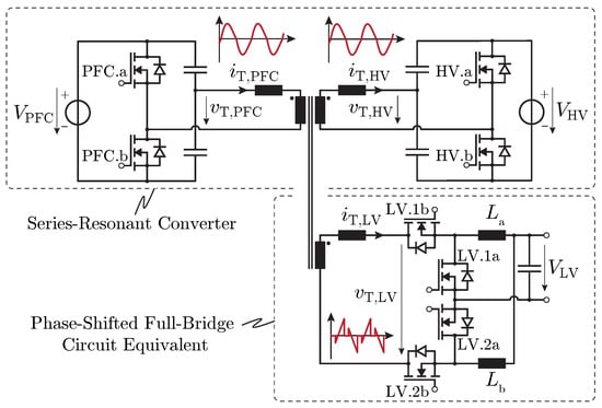
Figure 1.
Topology of the proposed three-port DC/DC converter comprising a resonant stage for the power flow from the output of an upstream PFC rectifier to the high-voltage (HV) battery and a phase-shifted full-bridge circuit equivalent, which controls the power flow to the low-voltage (LV) battery of the EV.
In Section 2, the general operation of the proposed converter topology is introduced and its advantages over existing solutions are discussed. Subsequently, Section 2.2 deals with the control of the LV-port and in particular with its impact on the ZVS operation of the PFC and HV-side power switches. In Section 3, the design of such a converter system for the exemplary specifications of Table 1 is discussed and its performance is finally verified in Section 4 by means of experimental measurements. Section 5 concludes the findings of this paper.

Table 1.
Specifications of the proposed three-port DC/DC converter.
2. General Converter Operation
In this section, the general operation of the converter in the two different modes of operation (CM and DM) are discussed and analyzed.
In a first step, only the SRC part of the converter is investigated, as it is only operated in CM and hardly any control is required. In a second step, the LV-port is also taken into account and its control is analyzed in detail.
2.1. Charge Mode Operation—Series-Resonant Converter
As already mentioned, the SRC is only operated in CM, where most of the power flows from the output of the PFC rectifier into the HV-battery and only a fraction is flowing from the PFC rectifier output to the LV-bus. Hence, in this mode, the converter is operated with full power for most of the time, which is why the converter should be designed in such a way, that the power transfer from the PFC rectifier output to the HV side is as efficient as possible. One of the most efficient topologies for such applications is a so-called DC-transformer [14], hence, a SRC which is operated with a fixed switching frequency close to the resonant frequency, resulting in a fixed voltage transfer ratio, which is given by the numbers of turns of the transformer. Consequently, the currents are all sinusoidal, whereby both, the high-frequency (HF) conduction losses as well as the EMI filtering effort are minimized. The only drawback of this topology is the fixed voltage transfer ratio, which inevitably leads to the necessity of a variable input voltage of the converter, which has to be adapted according to the required output voltage. In the application at hand, this is not really a drawback, as the whole system comprises of two independent stages, where the upstream PFC rectifier is capable of boosting the intermediate DC-link voltage to arbitrary voltage levels (possibly at the expense of higher required blocking voltages of the employed semiconductors in the PFC rectifier stage). Furthermore, by utilizing the PFC rectifier to indirectly control the output voltage through , the number of discrete inductive components of the complete converter system can be reduced, which is cost-wise a significant advantage. Hence, compared to conventional two-stage solutions with a fixed DC-link voltage , where one inductive component is used to bridge the voltage difference between the AC mains voltage and and another inductive component is used to bridge the difference between and the output voltage [15], only the inductive component in the PFC rectifier is used if the proposed DC-transformer stage is employed. Surprisingly, the inductor in the second stage can be saved with almost any size- or loss-penalty in the inductor of the PFC stage, as the component stresses of this component solely depend on the input voltage and the input power of the PFC rectifier, if triangular current mode (TCM) operation is used [16]. Thus, the current ripple in the input inductor is directly given by the input power of the converter (, ) and does not depend on the intermediate DC-link voltage . In contrast to the current ripple, however, the variable switching frequency in TCM is affected by the variable output voltage , according to
where , , and denote the mains frequency, the single-phase input voltage amplitude, the amplitude of the fundamental component of the input current and the inductance of the inductor in the PFC stage, respectively. Thus, the minimum switching frequency is slightly increasing with the output voltage , according to
Nevertheless, as the residual switching losses in TCM are small, the slightly higher average switching frequency does not harm the converter efficiency too much. Consequently, the only significant disadvantage of this approach are higher required breakdown voltages of the semiconductors in the PFC stage due to the variable output voltage . However, due to the availability of 900 wide band-gap semiconductor devices even with very low on-resistance [17,18], the single-inductor approach can be used for comparably wide input and output voltage ranges.
Thus, depending on the mains voltage and the required output voltage range, the turns ratio of the DC-transformer can now be chosen in such a way, that the minimum PFC-side referred output voltage is just larger than the peak of the AC input voltage .
In the application at hand, a turns ratio of has been chosen for simplicity reasons, but it should of course be adapted according to the specified mains voltage in a final product. However, this does not affect the operation of the system, which is why the aforementioned turns ratio of and the specifications of Table 1 are assumed in the further course of this paper.
Another advantage of the DC-transformer is its inherent voltage and power control, whereby only the input voltage of the converter needs to be regulated to its specified value, independent of the actual output power. This natural power balancing is shown in Figure 2 based on the simulated current and voltage waveforms. As illustrated in Figure 2a, the transformer current automatically reacts on a load step in the output current of the HV-port, by reducing its amplitude within a couple of cycles, before reaching its new stationary value. Due to the equal port voltages and and the synchronous operation of the PFC-side and the HV-side half-bridges, the applied voltage-time areas across the leakage inductance of the transformer are extremely small. Consequently, only a small resonant inductance is required, which is a particular advantage in designs with PCB-winding transformers, as the achievable leakage inductance in such transformers is strongly limited [19,20]. However, compared to conventional wire-wound transformers, PCB-winding transformers are much cheaper to manufacture and at the same time, the vertically aligned arrangement of the transformer windings mitigates HF conduction losses to a large extent [21,22]. Consequently, this sort of transformer should be used whenever possible and reasonable.
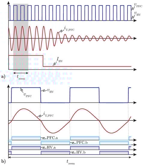
Figure 2.
(a) Voltage and current waveforms in the SRC part of the converter for a disconnected LV-port and a step in the output current of the HV-port. (b) Zoomed-in view of the aforementioned waveforms, including the gate signals of the power switches PFC.a, PFC.b, HV.a and HV.b.
To date, only the power flow from the PFC-port to the HV-port has been considered and the advantages and disadvantages of the selected topology have been highlighted. However, there is also a small power flow from the PFC-port to the LV-bus required, which is why a third transformer winding is necessary in order to be able to extract the power for the LV-bus directly from the common transformer core. Due to the extremely small leakage inductance in the PCB-winding transformer, the LV-sided winding voltage is given by and should not be forced to a different value, as otherwise, the resonant tank for the power flow from the PFC to the HV-port would be affected too much and the SRC would not work properly. However, as the LV-bus voltage varies between and 15 , at least one inductive component needs to be employed, which can take the voltage difference between and (cf. Figure 1). Consequently, the PFC output and the HV-port act as voltage sources, whereas the behavior of the LV-port corresponds to a current source due to the aforementioned inductive components. In order to control the power, which is extracted from the LV-winding, it is inevitable that the two output inductors and can be both, actively connected as well as actively disconnected to/from the LV-winding. This can be achieved by means of the proposed LV-sided circuit, whose simplified control is explained in the following.
2.2. Charge Mode Operation—Control of the LV-Port
The control of the LV-port power switches can be divided into two identical time intervals: The first half period (), where the LV-winding voltage is positive and can be applied to the LV-winding, and the second half period (), where is negative and can be applied to the LV-winding. Starting with the first half period and the initial conditions shown in Figure 3a,e, where the two currents in the output inductors and are circulating through the switches LV.1a and LV.2a, the switch LV.1b is blocking and prevents from being applied to . After a certain time , LV.1a is switched off and, due to the negative current in , the of LV.1a is charged until it reaches . Subsequently, the body diode of LV.1b starts to conduct, whereby this switch can be turned on under ZVS conditions. From now on, is directly applied to and the current in this inductor starts to increase again (cf. Figure 3b). At , the PFC-side and HV-side half-bridges are switched and becomes negative. Consequently, as , the current commutates back to the body diode of LV.1a, whereby this switch can be turned on under ZVS conditions as well. During the second half period, continues to circulate through LV.1a, which is why the active period , where the current in is increasing, cannot exceed a value of . If , LV.1a and LV.1b are considered as a conventional step-down converter, this statement is equivalent to allowing a maximum duty cycle of 50%. Hence, according to the well known formula for buck converters
the minimum winding voltage needs to be larger than twice the maximum LV-bus voltage in order to keep the required duty cycle below 50%. This limit sets the following constraint for the numbers of turns of the transformer windings:
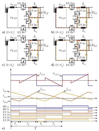
Figure 3.
(a–d) Current paths in the LV-port during the time intervals , and (e) the voltage and current waveforms in the LV-port including the gate drive signals of all power switches.
During the second half-period, where is negative, the second step-down converter (, LV.2a and LV.2b) is controlled exactly the same way as previously explained for , LV.1a and LV.1b. Hence, the only difference between the two sub-converter modules is, that their active periods are phase-shifted by 180.
Obviously, ZVS of LV.1b and LV.2b is only achieved, if the currents in the respective output inductors are negative before the switches are turned on. However, as the switching frequency in CM is given by the resonant frequency of the resonant tank between the PFC and the HV-port, and the duty cycle is defined by (3), there is no degree of freedom left, which would allow to control the current ripple in and during CM operation. Consequently, the current ripple can only be influenced during the design phase of the converter by an appropriate selection of the inductance value of and . The inductance should be selected in such a way, that ZVS for at least the maximum expected LV output power during CM ( 300 in this application) is guaranteed. However, a too small inductance results in a large current ripple and in unnecessary conduction losses in the LV-port, as this ripple current flows even for zero LV output power. This behavior is illustrated in Figure 3e, where the triangular currents and fluctuate around their average value with a constant ripple of , even if and therefore the LV output current are set to zero. Fortunately, this ripple current has a beneficial effect on the overall converter operation, as it assists the ZVS operation of the PFC and the HV-sided power semiconductors, as will be explained later in this paper.
2.3. Drive Mode Operation
In contrast to the charge mode (CM), there is no power flow in the PFC-port of the converter in drive mode (DM) operation, which is why the SRC is not operated anymore. Instead, the HV-port now actively applies a rectangular voltage to the transformer, as the power for the LV-bus is now drawn from the HV-battery. Consequently, the operating conditions for the LV-port do not change compared to the previously introduced CM operation, as there is again a rectangular voltage induced in the LV-winding. However, there is one important difference between the CM and the DM, as in DM, there is no resonant power transfer required and the constraint of a fixed switching frequency can therefore be loosened. Thus, the previously mentioned negative inductor currents during the switching transitions can now also be ensured for LV-output power values larger than 300 , as the switching frequency can be reduced, whereby the current ripple is increased.
Hence, the converter is controlled by means of a variable switching frequency and a duty cycle according to (3), as usually referred to as triangular current mode (TCM) operation [16,23] (cf. Figure 4). The optimum switching frequency can be calculated based on the momentary output current and the required ZVS current , according to
with
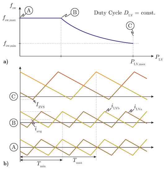
Figure 4.
(a) Switching frequency variation in drive mode for a constant output voltage and a varying output power and (b) the current waveforms for three exemplary output power levels Ⓐ, Ⓑ and Ⓒ.
The upper limit for the switching frequency is selected as the resonant frequency of the resonant tank between the PFC rectifier output and the HV-side, in order to limit the remaining switching losses during the dead times of the power switches and to avoid possible timing issues due to a limited PWM resolution of the control hardware. Nevertheless, this limit could of course also be increased if reasonable from an efficiency perspective.
To date, most of the components in the converter have been assumed to be ideal. However, in a real application, all the non-idealities of the components, as, e.g., the of the power switches, the parasitic inductances of all power tracks, etc. need to be considered as well. This is done in the following section and their impact on the converter operation is investigated in detail.
2.4. Impact of Parasitics on the Converter Control
The current source behavior of the LV-port, which can be connected/disconnected to/from the LV transformer winding, inevitably results in a problematic situation during the switching transitions, as the small, but still existing, leakage inductance of the LV transformer winding prevents current steps in . Hence, if is connected to the LV-winding with a non-zero current , would need to take over the momentary value of instantaneously. However, this would theoretically require an infinite voltage across the LV transformer winding, which would result in a voltage breakdown of LV.2a. Consequently, an additional small overvoltage circuitry is required, which acts as an energy buffer for the time required to equalize the two currents and (cf. Figure 5).
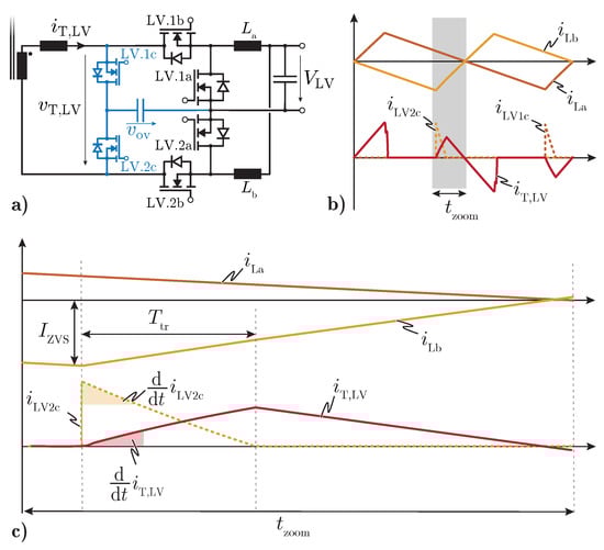
Figure 5.
(a) Additional overvoltage protection circuit (shown in blue) comprising the two small MOSFETs LV.1c and LV.2c, as well as the capacitor across which is applied. (b) LV-side current waveforms during one period and (c) zoomed-in view of the same waveforms during a switching transition.
As shown in Figure 5c, the current in the LV-winding starts at zero and should ideally immediately take over the current impressed in at the beginning of the switching transient. However, the gradient of the current rise of is given by
with
where denote the leakage inductance values of the respective transformer windings. Consequently, cannot take over immediately, as the capacitor voltage cannot be higher than the breakdown voltage of the LV power semiconductors. As a result, a current starts to flow in order to compensate for the difference between the two currents and . As soon as is equal to , is zero and the transition is completed. The time , which is required for this transition, depends on the initial negative current and can be calculated according to
Hence, the total charge which is flowing into the capacitor within one switching period is given by
In order to achieve a stable and therefore a stable charge balance in , the auxiliary switches LV.1c and LV.2c need to be actively connected to the transformer at some point in time, such that the same amount of charge is extracted, as otherwise, would continuously be increasing. The most intuitive solution would be to turn on LV.1c and LV.2c, whenever there is current flowing through their body diode, as this results in ZVS and therefore the most efficient operation of these switches. By keeping them turned on for a certain amount of time, the charge, which was injected due to the aforementioned current difference , is then fed back to the PFC and the HV-port by means of a resonant transition between , and the capacitive voltage dividers of the PFC and the HV-port. However, due to the small leakage inductance within the transformer, this yields very high peak currents in the auxiliary switches and at the same time unnecessary conduction losses in various components, as there is no advantage which could be taken from this reactive power flow.
Fortunately, the of these auxiliary switches is comparably small, whereby zero-current-switching (ZCS) operation of these semiconductors does not harm the efficiency of the converter too much. Thus, the capacitor can be connected to the transformer winding whenever required and reasonable. Keeping in mind, that the charge in can only be transferred to the PFC and the HV-port, as the leakage inductance values of the transformer are much smaller than the output inductors and , the only reasonable point in time to transfer this energy is during the switching transitions of the two aforementioned ports, as this additional energy supports the ZVS operation of the PFC and the HV-sided power semiconductors (cf. Figure 6).
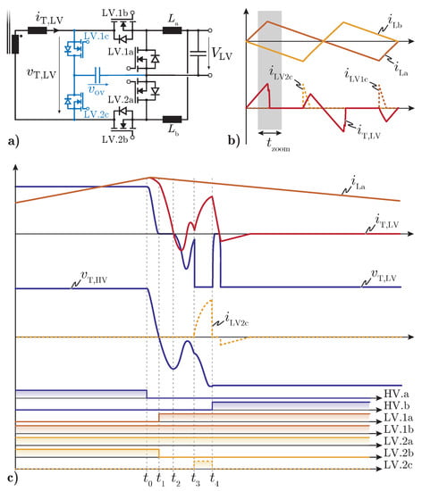
Figure 6.
(a) Overvoltage protection circuit (shown in blue) of the LV side with (b) the corresponding current waveforms during one period and (c) the zoomed-in view of the voltage and current waveforms during one ZVS transition.
For simplicity reasons, the ZVS transition is explained in the following for DM operation only, as in CM operation, the principle stays the same and the waveforms look similar.
Starting with the initial condition shown in Figure 6c at , the switching transition is initiated by turning off HV.a, whereby the inductor current starts to discharge the parallel connected of HV.a, HV.b and LV.1a, as follows . Consequently, and drop synchronously until reaches 0 . At this point (), the body diode of LV.1a starts to conduct and the inductor current commutates to LV.1a. Hence, due to , the HV-sided switch-node voltage equals , which is why only partial ZVS would be achieved. However, there is still magnetic energy stored in the leakage inductance of the transformer, which now starts to further charge/discharge the of the HV-sided half-bridge until . Thus, the larger the initial current is, the more likely a full charge/discharge of the HV-sided is achieved. Unfortunately, at , the voltages across the HV and the LV transformer windings are different, as is still zero, but is somewhere in between 0 and . This voltage difference initiates a resonant current through the leakage inductance of the transformer between the of the HV-port and the of LV.2b, which cannot be avoided and again increases (for ). Hence, it is impossible to ensure full ZVS with the magnetic energy only. At this point, the excess charge in comes into play, as LV.2c can be switched on in order to complete the HV-sided ZVS transition by generating an additional positive current pulse in , which charges/discharges the of the HV-side half-bridge completely (cf. ). However, this comes at the expense of additional switching losses in the LV-port, as the of LV.2b needs to be charged instantaneously from worst case 0 to through LV.1c. Nevertheless, the additional losses due to the comparably small of the LV power switches are still significantly lower than the switching losses, which would originate from incomplete ZVS of the HV power semiconductors.
After a certain on-time , the switch LV.2c is switched off again in order to minimize the RMS current stress in this component and to interrupt the discharging of . The actual length of the on-time is controlled in such a way, that the voltage always stays below the breakdown voltage of the LV power semiconductors, including a certain safety margin.
Furthermore, from an efficiency point of view, the time interval from to should be as short as possible, as the resonant current during this time interval serves no purpose and solely increases the conduction losses and extends the total dead time.
However, a certain delay is required, such that even for the maximum LV output currents, drops to zero before switching on LV.2c. This is important, as otherwise the small auxiliary switches LV.1c and LV.2c might need to take over the huge transformer currents during the switching transitions, which can easily go up to 200 . Consequently, the control effort can be minimized by keeping a constant , independent of the operating conditions, whereby ZVS of the PFC and HV semiconductors is guaranteed over the whole operating range. The optimal value of highly depends on the parasitics of the transformer design, the employed power semiconductors and the output inductors and are found easiest by means of simulation or experimental measurements.
Using this control strategy, the voltage and current waveforms in all the components can be calculated and/or simulated and the converter system can be designed accordingly. An exemplary design of such a converter is discussed in the following based on the specifications listed in Table 1.
3. Design of the Converter System
The design of the converter can be divided into three main stages, which highly depend on each other: First, the selection of the power semiconductors, second, the design of the three-winding transformer and third, the LV output inductors. Especially the design of the magnetic components has a significant impact on the current waveforms and, therefore, the arising conduction losses of the complete converter system. Consequently, the optimization of the overall converter is an iterative process with multiple sweep variables, as, e.g., the resonant frequency , the output inductance and the ratio between the resonant inductance and the resonant capacitor.
3.1. Power Semiconductors
Starting with the selection of the power semiconductors for the PFC and the HV-port, switches are required which feature a low on-state resistance for minimal conduction losses, as well as an as small as possible in order to reduce the ZVS effort. Considering the maximum DC-link voltage of 500 in both ports, the minimum required breakdown voltage is selected to be 600 . The most promising candidates are summarized in Figure 7a, where the vs. charge-equivalent performances are shown. These switches were finally considered in the optimization to find the most suitable PFC/HV power semiconductors.
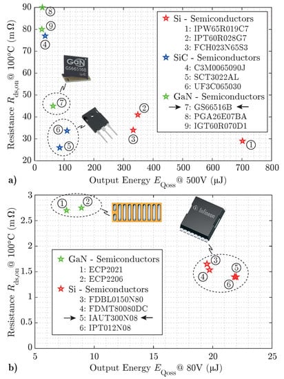
Figure 7.
(a) Most promising candidates for the semiconductors of the PFC and the HV-port and (b) the same graph for the LV power semiconductors.
The selection of the power switches for the LV-side not only depends on the output power, but also on the turns ratio n of the transformer, which directly defines the required minimum breakdown voltage of the switches LV., . Hence, in order to minimize the required total semiconductor chip area, an as low as possible breakdown voltage should be targeted [24]. However, the previously mentioned limitation of yields a lower limit for the minimum according to (3). Hence, the maximum PFC/HV-port voltage of 500 results in a of 60 , which is at the same time the minimum required breakdown voltage of the LV-switches. Similar to the PFC/HV semiconductors, as small as possible and values are in demand for minimizing the conduction and the switching losses in these components. Again, the most promising candidates are summarized in Figure 7b, which were considered in the final optimization.
3.2. Output Inductors
The design of the two output inductors depends on the resonant frequency and the desired LV current ripple in charge mode (CM) operation. The selection of inherently limits the maximum transferable power from the PFC to the LV-port, for which ZVS operation of all power semiconductors can be maintained (cf. Section 2).
Thus, should be at least 300 in this application, as this power is defined in the specifications as maximum LV output power in CM. However, the smaller the selected current ripple is, the wider the required switching frequency range in drive mode (DM) gets (cf. Figure 4). A wide switching frequency range, in turn, makes it more difficult to design an efficient and power-dense transformer, as will be discussed in the next section about the optimal design of the transformer. For this reason, , or equivalently , is considered as a degree of freedom in the overall converter optimization and for each a separate inductor optimization is conducted.
Based on and , the maximum current stresses for the inductor design can be calculated according to
where and denote the maximum DC current and the maximum total RMS current in the inductor, respectively. Hence, assuming a frequency independent resistance of the inductor winding, 75% of the arising conduction losses originate due to the DC component of the inductor current, according to
Consequently, an as small as possible DC-resistance of the winding is inevitable for an efficient converter operation. Due to cost reasons, all the magnetic components should be designed with PCB-integrated windings, as by doing so, the expensive wire-wrapping process of conventional manufacturing is omitted. However, the available copper in PCB windings is strongly limited, which is why the easiest way to achieve a low DC-resistance and at the same time a reasonable power density is, to solder additional copper foils to the top and the bottom layer of the PCB (cf. Figure 8a). Unfortunately, large copper planes in PCBs are prone to high-frequency (HF) effects, as, e.g., skin and proximity losses, which is why the inductor is designed according to the optimization described in [25], where the HF-effects are effectively mitigated by means of the fringing field around the air gap. Consequently, for each and , the performances of a large number of inductor designs with different winding widths , core cross-sections and numbers of turns are calculated and compared to each other (cf. Figure 8b). Finally, the most suitable inductor design is selected from the so-called Pareto front.
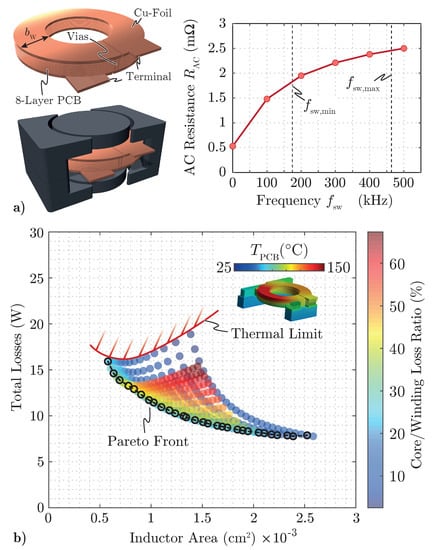
Figure 8.
(a) PCB winding inductor design with and the FEM-simulated winding resistance. (b) Pareto-optimization of a PCB-winding inductor with and , for varying winding widths , core cross-sections and numbers of turns . The most suitable inductor design is finally selected from the Pareto front.
3.3. Three-Winding Transformer
In order to start the design of the transformer, the turns ratio needs to be known. Due to the large currents in the LV-winding, only a single turn should be used in order to minimize the arising conduction losses. Consequently, the number of turns of the PFC and the HV-side winding can be calculated according to the specifications of Table 1 and the duty cycle limit given by (3) to be
Based on the number of turns and a certain output inductance , the minimum switching frequency in DM can be calculated according to
whereby the maximum flux linkage in the transformer core is inherently given by
The maximum flux linkage , together with the saturation flux density of a certain ferrite material, then yields a lower limit for the required magnetic core cross-section .
However, due to the wide switching frequency variation in DM, it is essential to select an appropriate core material, which performs well for both, high switching frequencies and low flux densities in CM, as well as low frequencies and high flux densities in DM. Ferroxcubes 3C98 has been found to be the most suitable ferrite material for this application, as it shows a comparably flat loss density throughout the whole switching frequency range, if the flux density varies inversely proportional to the frequency, according to (cf. Figure 9).
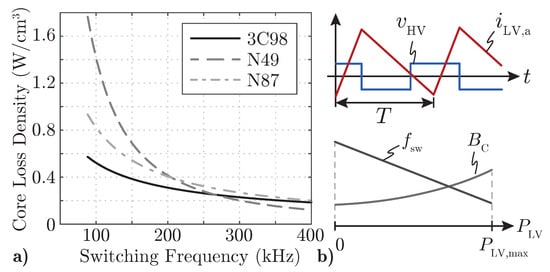
Figure 9.
(a) Magnetic core loss densities of three different materials for a frequency dependent flux density as shown in (b), where the switching frequency and the flux density variation for different LV output power values are illustrated.
This is equivalent to a Steinmetz parameter ratio of .
Similarly to the LV output inductors, a Pareto optimization can now be conducted based on the derived turns ratio n and the selected core material 3C98 for variable winding widths , core cross-sections and different winding layer arrangements.
However, in order to maximize the achievable leakage inductance between the PFC and the HV-side windings, which is required for the resonant tank in CM, the turns of these two windings should be separated as far as possible [19]. Furthermore, the large currents in the LV-winding demand for an extremely low winding resistance, which is why the available copper of a single PCB layer is not sufficient. Consequently, the top layer of the PCB has to be used as LV-winding, as it can be vertically extended by means of an additional copper foil which is soldered to it (cf. layer stack-up in Figure 10a). The remaining layers can therefore be used for the PFC and the HV-side winding as shown in Figure 10a. The shielding layer between the PFC and the HV-side winding does not carry any current and is solely used to assist the cooling of the PCB-winding by extracting the heat out of the transformer. As shown in Figure 10c, the proposed vertically aligned arrangement of the PCB-windings effectively mitigates the HF effects, whereby extremely low AC to DC resistance ratios result. Consequently, this arrangement was considered as the most promising one in the overall optimization.
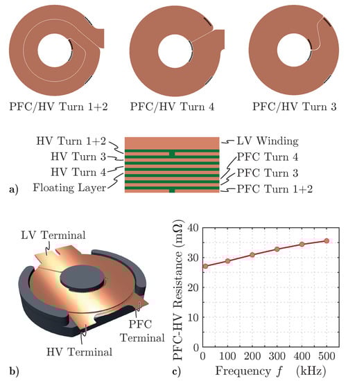
Figure 10.
(a) Layer stack-up and the design of the eight-layer PCB winding and (b) the corresponding 3D model. (c) The FEM-simulated frequency dependent total winding resistance of the PFC and the HV-side winding (sum of the two).
The leakage inductance values of a specific transformer design can be calculated as introduced in [20] and inherently define the required resonant capacitance according to
where denotes the total leakage inductance between the PFC and the HV-side winding.
Hence, the derived transformer model, the inductor optimization as well as the semiconductor pre-selection can now be used for the Pareto optimization of the overall converter system.
Thus, for different , and therefore , the arising losses in the magnetic components, as well as the losses in the power semiconductors can be derived and are then set in relation to the total required PCB area of the transformer, which is by far the largest power component of the converter and therefore is a good measure to estimate the power density of the overall converter system.
The results are shown in Figure 11 for full-power operation in CM, hence a power flow of from the PFC to the HV-port and zero power from the PFC to the LV-port. Thus, only the current ripple with 0 offset is circulating in the LV-port, which ensures the necessary ZVS of the PFC and the HV-side power semiconductors. The additional conduction losses due to this circulating current in the LV-port are indicated by means of the colors of the different converter designs, whereby these losses are an optimistic estimate, as for simplicity reasons, only the losses in the main power components, but not in the connecting PCB tracks in between these components are considered. In the same figure, the red circle specifies the converter design, which has finally been selected for hardware implementation, in order to experimentally verify the performance and the suitability of the proposed topology. The estimated efficiencies of the selected converter design are summarized in Figure 12 for full-load operation in CM (a), partial-load operation in DM (b) and full-load operation in DM (c).
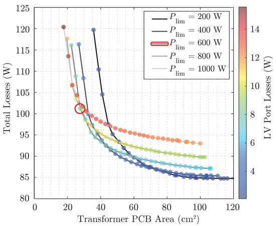
Figure 11.
Calculated Pareto fronts for different , a power flow of from the PFC to the HV-port and 0 from the PFC to the LV-port, hence, only the ripple current is flowing in the LV-port. The colors of the dots indicate the amount of losses, which are induced in the LV-port due to these circulating currents.
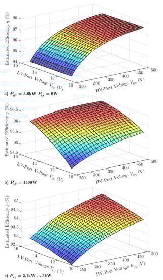
Figure 12.
Calculated efficiencies of the selected converter design for an output power of (a) and in charge mode (CM) operation, (b) in drive mode (DM) operation and (c) in DM operation, which is limited by the maximum allowed output current of .
In DM especially the partial-load efficiency is of importance, as the converter is operated most of the time with a partial load of 30–50%. In contrast, an as high as possible full-load efficiency in CM is required, as during the charging process, the converter is operated at full load almost all the time. However, as already mentioned, these efficiencies are a very optimistic estimate, as in the real hardware prototype, the huge LV-port currents do not only flow through the LV-winding and the LV-inductors, which are considered in the efficiency calculation, but also in the connecting PCB tracks and the necessary vias, where substantial additional conduction losses are induced. Unfortunately, these losses cannot reasonably be considered in the optimization, as they highly depend on the final PCB design. Consequently, much higher LV-sided conduction losses and therefore a lower overall efficiency is expected in the hardware prototype.
4. Experimental Verification
Based on the results of the aforementioned optimization, the most promising design has finally been implemented in hardware to test the suitability of the proposed converter topology. The characteristic parameters of the selected converter design are summarized in Table 2 and the employed power components of the individual converter ports are listed in Table 3. Furthermore, the complete converter is controlled by means of a STM32F303 DSP in combination with a small MachXO2 FPGA, which generates the different gate signals and ensures the appropriate dead times.
Table 2.
Operating parameters of the three-port DC/DC converter hardware prototype.
Table 3.
Component specifications of the three-port DC/DC converter hardware prototype.
The hardware design of the PCB-winding transformer corresponds to the one shown in Figure 10b with a winding width of 13 , whereby the PCB-winding is implemented in an 8-layer 70 PCB with an overall thickness of (for isolation purposes).
Furthermore, the thickness of the additional copper foil for the LV-winding is and the minimum core cross-section is 290 2 (cf. Figure 13a).
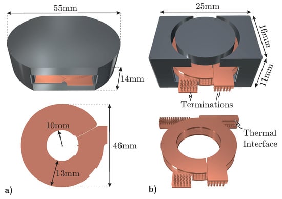
Figure 13.
(a) Dimensions of the PCB-winding transformer of the hardware prototype and (b) the dimensions of the employed PCB-winding inductor.
The two capacitive voltage dividers of the PFC and the HV-port comprise 16 individual 100 SMD capacitors (C4532NP02E104) each (8 on the top layer and 8 on the bottom layer of the PCB), in order to minimize the total ESR of the capacitor banks and, therefore, the arising conduction losses as well.
Hence, each capacitive voltage divider consists of two equivalent 800 capacitors, whereby the total effective resonant capacitance between the PFC and the HV-port is 800 as well. This resonant capacitance, in combination with the expected total leakage inductance between the PFC and the HV-port of 142 , results in the targeted resonant frequency of .
The inductance of the output inductors is given by the optimized design as , which is why the minimum switching frequency can be calculated according to (14) to be .
The dimensions of the PCB-winding inductor design are summarized in Figure 13b, where the thickness of the additional copper foil on the top and on the bottom layer is again . In order to improve the thermal coupling between the inductor winding and the heat sink, additional thermal interfaces are used, which are directly attached to the water-cooled heat sink through galvanically isolating thermal interface materials (TIM-Bergquist Gap Pad TGP HC5000). The additional copper foils for the LV inductor winding, on top and on the bottom of the PCB, are extended towards the output capacitors of the LV-port, in order to minimize the overall resistance of the current paths, as shown in Figure 14, where the fully assembled converter and the dimensions of the complete hardware prototype (including heat sink volume) are depicted. The water-cooled aluminum heat sink (not visible in this figure) covers the complete bottom side of the converter and is screwed to the PCB in order to optimize the thermal interface between the PCB and the heat sink and to ensure short thermal paths from each component to the aforementioned common heat sink.
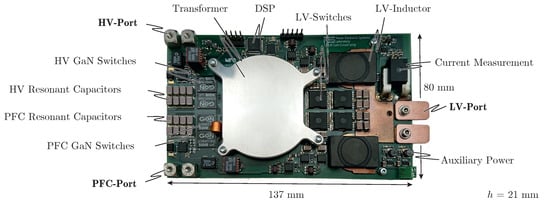
Figure 14.
Hardware prototype of the three-port converter system with a total height of (including heat sink volume).
4.1. Measured Waveforms in CM
The experimentally measured waveforms in charge mode (CM) operation are shown in Figure 15 for exemplary full-load operating conditions with port voltages according to , and and a power flow of from the PFC to the HV-port and 300 from the PFC to the LV-port. It should be mentioned, that the switching frequency in CM in the hardware demonstrator was set to 430 instead of 470 , as the measured total series-resonant inductance was slightly higher than the calculated , as the connection from the switch-nodes of the half-bridges to the transformer windings also contribute to the total series-resonant inductance. Consequently, the measured resonant frequency is somewhat lower, which is why the converter was operated with a switching frequency of 430 only. Furthermore, it can be noticed, that almost the full LV winding current is mapped to the HV-winding, whereby the PFC winding current is not really affected by the LV-port. This asymmetry originates from the fact, that the coupling between the HV and the LV-winding is much stronger than the coupling between the PFC and the LV-winding, as the distance between the PFC and the LV-winding is more than twice the distance between the HV and the LV-winding.
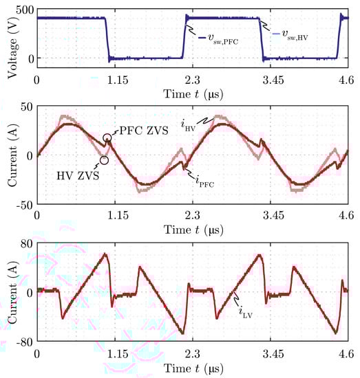
Figure 15.
Experimentally measured PFC-sided switch-node voltage and the three winding currents , and of the PCB winding transformer for nominal operation in CM with , , and .
However, this asymmetry is intended, as due to this winding arrangement, during the switching transitions of the PFC and the HV-port, the switch-node currents and have different signs. Consequently, absolutely synchronous ZVS transitions of the two switch-node voltages and are achieved, as the of the two half-bridges are synchronously charged/discharged. This is important, as otherwise, a comparably large voltage-time area () across the small resonant inductance would be applied, yielding a distortion of the resonant currents and during the transitions. Thus, the proposed layer stack-up of Figure 10a should always be used for this topology, if a proper ZVS performance of the converter should be guaranteed.
It needs to be mentioned, that due to the high level of system integration of the hardware demonstrator, only the PFC-sided transformer current can be measured accurately by means of a Rogowski current transducer (PEM CWT Ultra-mini, attached around the orange copper loop in Figure 14). The HV and the LV-sided currents and were measured by means of a current sniffer probe (AimTTi I-Prober 520), which allows for contactless measurement of a current in a PCB track, based on its surrounding magnetic field. However, this method can only be used for a qualitative measurement, as a quantitative measurement, even with calibration, is extremely difficult in a densely packed converter. Fortunately, the magnitudes of the contactless measurements and can easily be estimated based on the accurate PFC current measurement .
The experimentally measured efficiency curves in CM for nominal LV-port operation ( and ) and variable HV output power , for the maximum and the minimum HV-port voltage are shown in Figure 16. For the nominal HV-port voltage (), a high full-load efficiency is achieved, as the 650 semiconductors are optimally utilized, with a high voltage and a comparably low current. However, the efficiency drops significantly for partial-load operation, as the peak-to-peak value of the circulating current in the LV-port is proportional to and, therefore, results in a large constant loss-offset, which gains more and more impact on the efficiency, the lower the total output power is. Nevertheless, this was expected beforehand as it is a characteristic behavior of this topology. For the minimum HV-port voltage (), however, the picture changes completely. Hence, the full-load efficiency is comparably low, as the 650 semiconductors are poorly utilized due to the low voltage and the resulting high currents, whereby the achievable efficiency is mainly limited by the conduction losses in these components. In contrast, the low reduces the circulating current in the LV-port, whereby the partial-load efficiency is significantly increased. However, all the measured efficiencies are slightly lower than the calculated efficiencies for the ideal system, which has mainly two reasons: On the one hand, the conduction losses in the LV-port are much higher than calculated, due to the previously mentioned additional current paths on the PCB, which are required to interconnect the various LV-sided power components. On the other hand, the junction temperatures and the respective temperature dependent of the power semiconductors were calculated in the optimization based on the thermal model of the ideal thermal path from the semiconductor package to the heat sink (including thermal vias and TIMs). However, in reality, the idealized calculated thermal resistances can hardly be achieved, as the employed semiconductor packages are designed for bottom-side cooling, whereby all the semiconductor losses need to be dissipated through thermal vias in the PCB and through the galvanically isolating TIM into the heat sink. Unfortunately, all these thermal vias in the footprints of the power switches make it more difficult to properly solder the switches to the PCB, as most of the solder paste is extracted through these vias during the reflow soldering process. Consequently the assumed ideal attachment of the switches to the PCB is hardly achieved, whereby the resistances of the thermal paths are increased. Consequently, the junction temperatures, as well as the , were slightly underestimated in the optimization, which has a significant impact on the arising conduction losses, especially for GaN semiconductors. For this reason, it might be beneficial to use top-side cooled semiconductor packages, as both, the solder joints as well as the thermal coupling between the switches and the heat sink would be improved (at the expense of a more complex heat sink design).
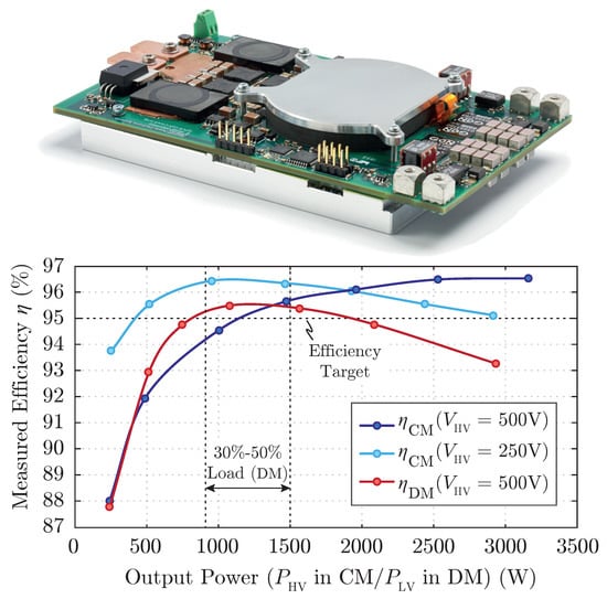
Figure 16.
Experimentally measured converter efficiencies in CM for the maximum and the minimum HV-port voltage and a constant output power in the LV-port of at . Furthermore, the efficiency in DM for a of 500 and a of 15 is shown. The efficiency targets of 95% at full load in CM, as well as partial load in DM are easily met.
Nevertheless, the efficiency target of 95% at full load in charge mode is easily met, whereby the proposed topology has been proven to be a reasonable solution for three-port EV charging applications. In the following subsection, the converter performance is investigated in the second operating mode, the drive mode operation.
4.2. Measured Waveforms in DM
The experimentally measured waveforms in drive mode (DM) operation are shown in Figure 17, for exemplary partial-load operating conditions according to , and . In order to ensure ZVS of the LV-sided semiconductors, the switching frequency is set according to (5) to , whereby ZVS is guaranteed and at the same time the conduction losses are minimized.
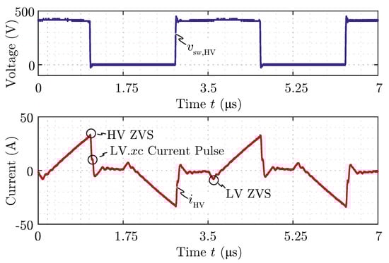
Figure 17.
Experimentally measured HV-sided switch-node voltage and the HV winding current of the PCB-winding transformer for nominal operation in DM with , and .
Furthermore, the additional short current pulses through the auxiliary switches LV.xc, , during each HV-sided switching transition can be observed. It needs to be mentioned, that the correct timing of the LV.xc switches is extremely important in a real system, as a slightly too early turn-on of these switches significantly increases the arising conduction losses in them. In contrast, a delayed turn-on in DM does not really have a negative effect on the operation of the converter, as there is no resonant current flow in the transformer, which could be distorted by an asynchronous switching transition of the PFC and the HV-sided half-bridges.
However, in CM, a delayed switching transition indeed distorts the resonant current from the PFC to the HV-side, which in worst-case could lead to a destabilization of the resonant operation, as mentioned in the previous section. Hence, an extremely precise timing is especially important in CM, but unfortunately also very challenging to achieve.
In order to circumvent the timing issue, if, e.g., a slow DSP or FPGA should be employed, passive diodes can be used instead of LV.xc, whereby the excess charge in needs to be transferred to the LV-port by means of an additional circuitry. In case of only small (10), a Zener diode () can be connected between the positive potential and the positive potential, which keeps at (cf. Figure 18a). This is the simplest and most reliable solution, but at the same time also quite inefficient, as a large fraction of is dissipated in the Zener diode. Hence, for large , it might be better to employ a simple additional miniature step-down converter, which keeps at a specified level and feeds the excess energy to (cf. Figure 18b). Even though these additional auxiliary circuits slightly increase the total number of components of the converter, the partial-load efficiency could be significantly increased, as the arising switching losses during the switching actions of LV.xc (due to the of LV.xc and LV.xb) could be circumvented.
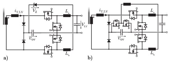
Figure 18.
Alternative over-voltage protection circuits using (a) two passive diodes and a Zener diode and (b) two passive diodes and an additional miniature step-down converter.
However, with an appropriate control hardware, the two auxiliary switches can be controlled as described in Section 2.2, whereby the experimentally measured efficiency of Figure 12 (red line) for the nominal port voltages and and a variable can be found. Similar to the efficiency curves in CM, two main loss mechanisms can be observed: On the one hand, the inherently given circulating current in the LV-port reduces the achievable low-load efficiency, whereby the huge currents in full-load operation induce substantial overall conduction losses in the converter, limiting the achievable full-load efficiency. Nevertheless, the targeted partial-load efficiency of 95% in nominal operation can still be met, whereby the proposed topology has also be proven to be a reasonable solution in drive mode operation.
A direct comparison of the performance of this new topology with state-of-the-art solutions is not trivial at this point, as the integration of the single-phase on-board charger with the DC/DC step-down converter is not yet a widely used industry standard. Consequently, hardly any systems with similar specifications have been presented in the literature so far with which the proposed topology could be compared. Nevertheless, it is possible to get a good impression of the performance of the system presented by comparing the efficiency and power density with an isolated two-port DC/DC converter with similar specifications [13] (PCB-integrated magnetics, 3 , , ), which could be used in EV applications as supply for the LV-bus. It is found, that both the power density ( vs. ) and the efficiency (95.6% vs. 96.6%) are only slightly lower in the three-port system, even though there is an additional isolated power path ( ) between the PFC and the HV port included. Thus, with the proposed three-port DC/DC converter and an additional non-isolated PFC rectifier, a complete three-port EV charger could easily be built. In order to obtain the same functionality with the two-port converter of [13], not only an additional non-isolated PFC rectifier, but also an isolated DC/DC converter between the PFC port and the HV port would be required. Taking into account the power densities mentioned above, this would mean that the additional DC/DC converter should have a maximum volume of so that in the end both chargers would be the same size. However, the additional converter can hardly be built so small and at the same time efficient enough, which is why the proposed three-port system has clear advantages in terms of size.
Even though the proposed topology is perfectly suitable for the application at hand, there is still room for improvement in terms of hardware implementation, as especially the partial-load efficiency in nominal CM operation is limited by the large circulating currents in the LV-port. Hence, in order to increase the partial-load efficiency in CM, somewhat larger output inductors should be used, whereby the peak-to-peak and the RMS value of the current ripple is reduced. However, this would require a larger transformer core cross-section, resulting in a reduction of the power density of the converter. Furthermore, a more sophisticated cooling concept might be beneficial, where either top-side cooled packages of the power semiconductors are used, which are then connected to the common heat sink by means of heat pipes, or cold welding instead of soldering of the switches could be used, in order to improve the joint between the switches and the PCB, whereby the thermal resistance from the semiconductor chip to the heat sink is significantly reduced. However, the application of these methods is always a tradeoff between additional manufacturing costs and the achievable advantages in terms of system performance.
5. Conclusions
In this paper, a novel three-port DC/DC converter topology for automotive applications has been proposed and analyzed. The topology comprises a combination of a series-resonant converter (SRC), which interconnects the DC-link capacitor of an upstream PFC rectifier with a high-voltage (HV) battery, and a modified phase-shifted full-bridge (MPSFB) converter, which connects the aforementioned HV-battery with an auxiliary low-voltage (LV) battery. The two sub-systems are controlled synergetically, as they share a common transformer core, whereby the MPSFB can be used to ensure zero-voltage-switching (ZVS) and absolutely synchronous switching transitions of the PFC- and the HV-sided half-bridges in the SRC. It is shown, that due to the aforementioned synchronous switching transitions, an extremely small series-resonant inductance can be used, which is particularly beneficial, if the leakage inductance of conventional PCB-winding transformer structures should be used as series-resonant inductance. In order to facilitate a possible hardware implementation of the proposed topology, simple design guidelines are given and the ideally achievable converter performance is found based on a multi-objective optimization. Finally, the suitability of the proposed converter topology has been proven by means of a 500 / 500 / 15 hardware demonstrator with a power density of , which easily meets the targeted full-load efficiency of 95% for nominal operating conditions (maximum port voltages) in charge mode (CM), and the partial-load efficiency of 95% for nominal operating conditions in drive mode (DM).
Author Contributions
Conceptualization, J.S. and J.W.K.; methodology, J.S.; validation, J.S. and J.W.K.; formal analysis, J.S.; investigation, J.S. and J.W.K.; writing—original draft preparation, J.S.; writing—review and editing, J.S. and J.W.K.; supervision, J.W.K.; project administration, J.W.K. All authors have read and agreed to the published version of the manuscript.
Funding
This research was funded by Robert BOSCH GmbH.
Data Availability Statement
Data presented in this studyare available on request from the corresponding author. The data are not publicly available due to internal policies of the industry research partner.
Acknowledgments
The authors would like to thank the Robert BOSCH GmbH for supporting this research project, and in particular Thomas Plum, BOSCH Corporate Research, for several inspiring technical discussions.
Conflicts of Interest
The authors declare no conflict of interest.
References
- Fast Charging Just Got Faster. High Power for Next Generation Electric Vehicles (350 kW). Available online: https://new.abb.com/ev-charging/products/car-charging/high-power-charging (accessed on 9 June 2020).
- High Power Charging (350 kW). Available online: https://www.allego.eu/business/high-power-charging (accessed on 9 June 2020).
- Introducing V3 Supercharging. Available online: https://www.tesla.com/blog/introducing-v3-supercharging (accessed on 9 June 2020).
- Krismer, F.; Kolar, J.W. Efficiency-optimized high-current dual active bridge converter for automotive applications. IEEE Trans. Ind. Electron. 2012, 59, 2745–2760. [Google Scholar] [CrossRef]
- Krishnaswami, H.; Mohan, N. Three-Port Series-Resonant DC–DC Converter to Interface Renewable Energy Sources With Bidirectional Load and Energy Storage Ports. IEEE Trans. Power Electron. 2009, 24, 2289–2297. [Google Scholar] [CrossRef]
- Tao, H.; Duarte, J.L.; Hendrix, M.A.M. Three-Port Triple-Half-Bridge Bidirectional Converter With Zero-Voltage Switching. IEEE Trans. Power Electron. 2008, 23, 782–792. [Google Scholar]
- Zhao, C.; Round, S.D.; Kolar, J.W. An Isolated Three-Port Bidirectional DC-DC Converter With Decoupled Power Flow Management. IEEE Trans. Power Electron. 2008, 23, 2443–2453. [Google Scholar] [CrossRef]
- Jakka, V.N.S.R.; Shukla, A.; Demetriades, G.D. Dual-Transformer-Based Asymmetrical Triple-Port Active Bridge (DT-ATAB) Isolated DC–DC Converter. IEEE Trans. Ind. Electron. 2017, 64, 4549–4560. [Google Scholar] [CrossRef]
- Liu, R.; Li, Z. A Three-Port Multi-Element Resonant Converter with Decoupled Power Flow Management. In Proceedings of the IEEE 4th Southern Power Electronics Conference (SPEC), Singapore, 10–13 December 2018. [Google Scholar]
- Al-Soeidat, M.; Khawladeh, H.; Aljarajreh, H.; Lu, D. A Compact Three-Port DC-DC Converter for Integrated PV-Battery System. In Proceedings of the IEEE International Power Electronics and Application Conference and Exposition (PEAC), Shenzhen, China, 4–7 November 2018. [Google Scholar]
- Wu, Y. Novel High Efficiency Three-Port Bidirectional Step-up/Step-down DC/DC Converter for Photovoltaic Systems. Sustainability 2021, 13, 7913. [Google Scholar] [CrossRef]
- Sim, J.; Lee, J.; Choi, H.; Jung, J. High Power Density Bidirectional Three-port DC-DC Converter for Battery Applications in DC microgrids. In Proceedings of the IEEE 10th International Conference on Power Electronics (ECCE Asia), Busan, Korea, 27–30 May 2019. [Google Scholar]
- Knabben, G.; Zulauf, G.; Schäfer, J.; Kolar, J.W.; Kasper, M.; Azurza, J.A.; Deboy, G. Conceptualization and Analysis of a Next-Generation Ultra-Compact 1.5-kW PCB-Integrated Wide-Input-Voltage-Range 12V-Output Industrial DC/DC Converter Module. Electronics 2021, 10, 2158. [Google Scholar] [CrossRef]
- Tran, Y.K.; Freijedo, F.D.; Dujic, D. Open-loop power sharing characteristic of a three-port resonant LLC converter. CPSS Trans. Power Electron. Appl. 2019, 4, 171–179. [Google Scholar] [CrossRef]
- Everts, J.; Krismer, F.; Van den Keybus, J.; Driesen, J.; Kolar, J.W. Comparative evaluation of soft-switching, bidirectional, isolated AC/DC converter topologies. In Proceedings of the IEEE Applied Power Electronics Conference and Exposition (APEC), Orlando, FL, USA, 5–9 February 2012. [Google Scholar]
- Kaufmann, M.; Tüysüz, A.; Kolar, J.W. New optimum modulation of three-phase ZVS triangular current mode GaN inverter ensuring limited switching frequency variation. In Proceedings of the 8th IET International Conference on Power Electronics, Machines and Drives (PEMD), Glasgow, UK, 19–21 April 2016. [Google Scholar]
- Transphorm 900 V Gallium Nitride FET. Available online: https://www.transphormusa.com/en/products/900v/ (accessed on 9 December 2020).
- Wolfspeed 900 V Silicon Carbide MOSFETs. Available online: https://www.wolfspeed.com/900v-silicon-carbide-mosfets (accessed on 9 November 2020).
- Ouyang, Z.; Thomsen, O.C.; Andersen, M.A.E. The Analysis and Comparison of Leakage Inductance in Different Winding Arrangements for Planar Transformer. In Proceedings of the International Conference on Power Electronics and Drive Systems (PEDS), Taipei, Taiwan, 2–5 November 2009. [Google Scholar]
- Zhang, J.; Ouyang, Z.; Duffy, M.C.; Andersen, M.A.E.; Hurley, W.G. Leakage Inductance Calculation for Planar Transformers With a Magnetic Shunt. IEEE Trans. Ind. Appl. 2014, 50, 4107–4112. [Google Scholar] [CrossRef] [Green Version]
- Ouyang, Z.; Thomsen, O.C.; Andersen, M.A.E. Optimal Design and Tradeoff Analysis of Planar Transformer in High-Power DC–DC Converters. IEEE Trans. Ind. Electron. 2012, 59, 2800–2810. [Google Scholar] [CrossRef]
- Zhang, J.; Hurley, W.G.; Wolfle, W.H.; Duffy, M.C. Optimized Design of LLC Resonant Converters Incorporating Planar Magnetics. In Proceedings of the IEEE Applied Power Electronics Conference and Exposition (APEC), Long Beach, CA, USA, 17–21 March 2013. [Google Scholar]
- Haryani, N.; Ohn, S.J.; Hu, J.; Rankin, P.; Burgos, R.; Boroyevich, D. A Novel ZVS Turn-on Triangular Current Mode Control with Phase Synchronization for Three Level Inverters. In Proceedings of the IEEE Energy Conversion Congress and Exposition (ECCE), Portland, OR, USA, 23–27 September 2018. [Google Scholar]
- Kasper, M.; Bortis, D.; Kolar, J.W. Scaling and balancing of multi-cell converters. In Proceedings of the IEEE International Power Electronics Conference (IPEC ECCE Asia), Hiroshima, Japan, 18–21 May 2014. [Google Scholar]
- Schäfer, J.; Bortis, D.; Kolar, J.W. Novel Highly Efficient/Compact Automotive PCB Winding Inductors Based on the Compensating Air-Gap Fringing Field Concept. IEEE Trans. Power Electron. 2020, 35, 9617–9631. [Google Scholar] [CrossRef]
Publisher’s Note: MDPI stays neutral with regard to jurisdictional claims in published maps and institutional affiliations. |
© 2021 by the authors. Licensee MDPI, Basel, Switzerland. This article is an open access article distributed under the terms and conditions of the Creative Commons Attribution (CC BY) license (https://creativecommons.org/licenses/by/4.0/).