
An Efficient 4H-SiC Photodiode for UV Sensing Applications

 ,
,  ,
, 
Abstract
:1. Introduction
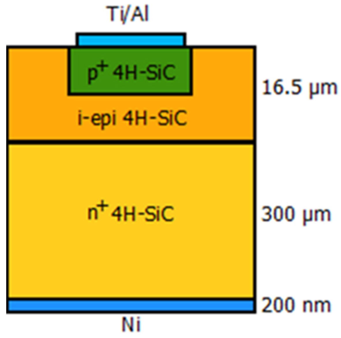
2. Experiments
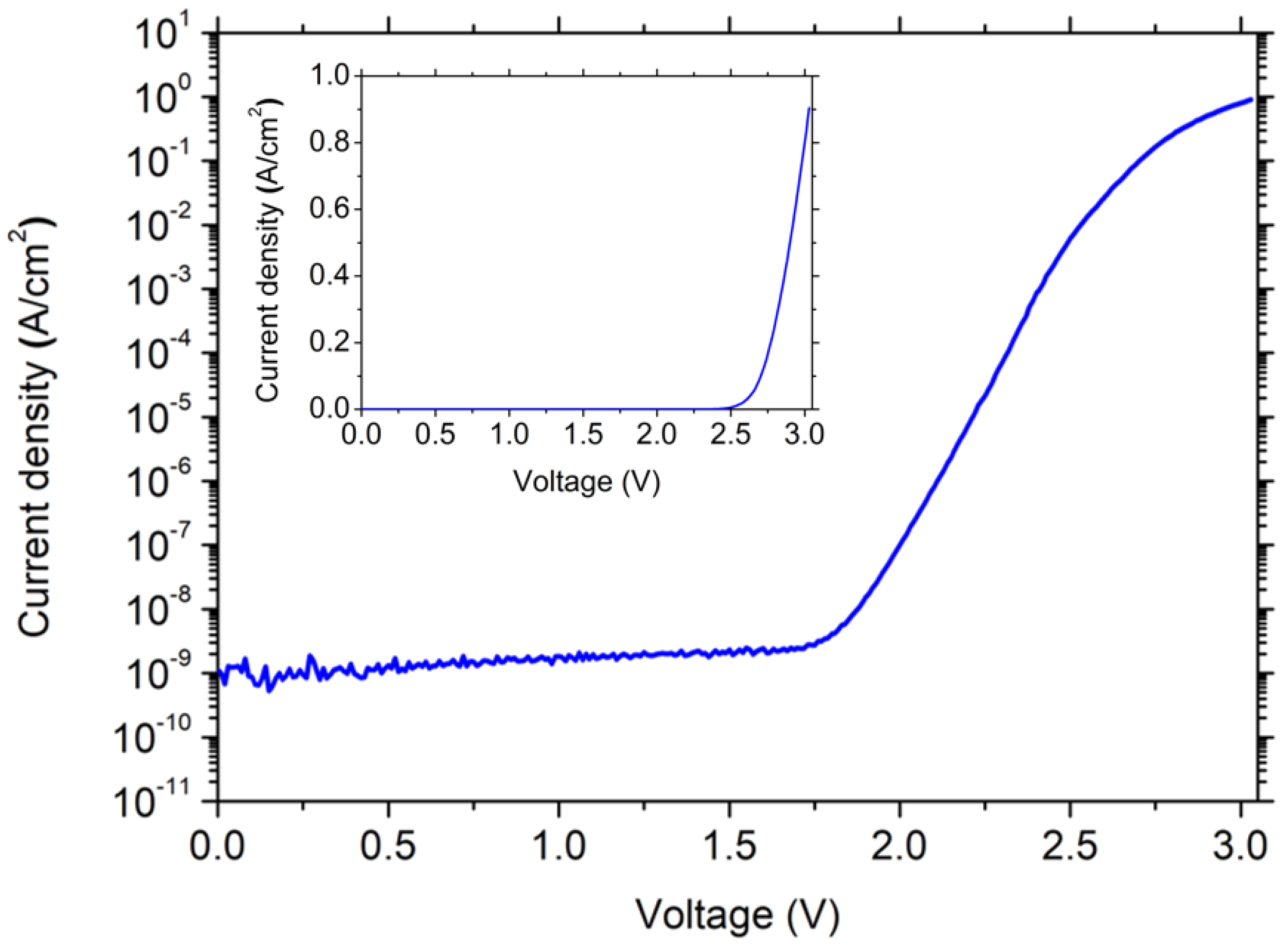
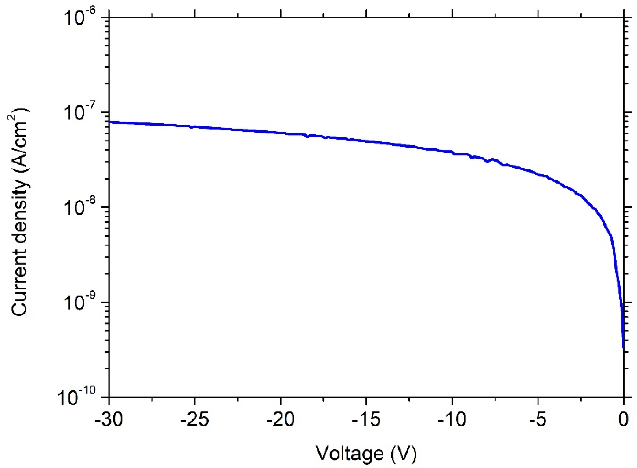
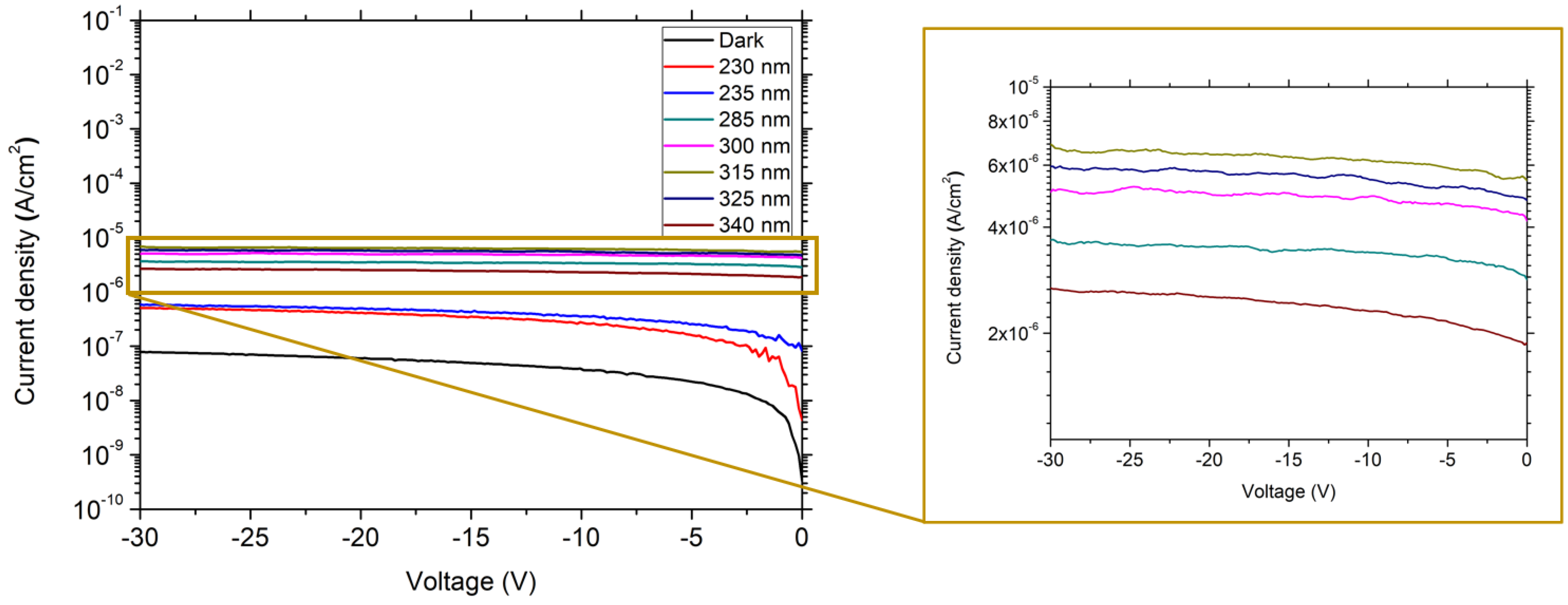
3. Results and Discussions
4. Analysis of High-Temperature Effects
5. Conclusions
Author Contributions
Funding
Data Availability Statement
Acknowledgments
Conflicts of Interest
References
- Chen, X.; Ren, F.; Gu, S.; Ye, J. Review of gallium-oxide-based solar-blind ultraviolet photodetectors. Photonics Res. 2019, 7, 381–415. [Google Scholar] [CrossRef]
- Araujo, H.M.; Chepel, V.Y.; Lopes, M.I.; Marques, R.F.; Policarpo, A.J.P.L. Low temperature performance of photomultiplier tubes illuminated in pulsed mode by visible and vacuum ultraviolet light. Rev. Sci. Instrum. 1997, 68, 34–40. [Google Scholar] [CrossRef]
- De Arquer, F.P.G.; Armin, A.; Meredith, P.; Sargent, E.H. Solution-processed semiconductors for next-generation photodetectors. Nat. Rev. Mater. 2017, 2, 16100. [Google Scholar] [CrossRef] [Green Version]
- Zhou, D.; Liu, F.; Lu, H.; Chen, D.; Ren, F.; Zhang, R.; Zheng, Y. High-temperature single photon detection performance of 4H-SiC avalanche photodiodes. IEEE Photonics Technol. Lett. 2014, 26, 1136–1138. [Google Scholar] [CrossRef]
- Sozzi, G.; Puzzanghera, M.; Menozzi, R.; Nipoti, R. The role of defects on forward current in 4H-SiC pin diodes. IEEE Trans. Electron Devices 2019, 66, 3028–3033. [Google Scholar] [CrossRef]
- Hou, S.; Hellström, P.; Zetterling, C.; Östling, M. 550 °C 4H-SiC p-i-n Photodiode Array with Two-Layer Metallization. IEEE Electron Device Lett. 2016, 37, 1594–1596. [Google Scholar] [CrossRef]
- Hou, S.; Hellström, P.; Zetterling, C.; Östling, M. Scaling of 4H-SiC p-i-n photodiodes for high temperature applications. In Proceedings of the 2017 75th Annual Device Research Conference (DRC), South Bend, IN, USA, 25–28 June 2017; pp. 1–2. [Google Scholar]
- Sang, L.; Liao, M.; Sumiya, M. A comprehensive review of semiconductor ultraviolet photodetectors: From thin film to one-dimensional nanostructures. Sensors 2013, 13, 10482–10518. [Google Scholar] [CrossRef]
- Bencherif, H.; Dehimi, L.; Messina, G.; Vincent, P.; Pezzimenti, F.; Della Corte, F.G. An optimized Graphene/4H-SiC/Graphene MSM UV-photodetector operating in a wide range of temperature. Sens. Actuators A Phys. 2020, 307, 112007. [Google Scholar] [CrossRef]
- Seely, J.F.; Kjornrattanawanich, B.; Holland, G.E.; Korde, R. Response of a SiC photodiode to extreme ultraviolet through visible radiation. Opt. Lett. 2005, 30, 3120–3122. [Google Scholar] [CrossRef]
- Rao, S.; Pangallo, G.; Della Corte, F.G. 4H-SiC p-i-n diode as Highly Linear Temperature Sensor. IEEE Trans. Electron Devices 2016, 63, 414–418. [Google Scholar] [CrossRef]
- Rao, S.; Pangallo, G.; Della Corte, F.G. Highly Linear Temperature Sensor Based on 4H-Silicon Carbide p-i-n diodes. IEEE Electron Device Lett. 2015, 36, 1205–1208. [Google Scholar] [CrossRef]
- Rao, S.; Pangallo, G.; Pezzimenti, F.; Della Corte, F.G. High-performance temperature sensor based on 4H-SiC Schottky diodes. IEEE Electron Device Lett. 2015, 36, 720–722. [Google Scholar] [CrossRef]
- Zeghdar, K.; Dehimi, L.; Pezzimenti, F.; Rao, S.; Della Corte, F.G. Simulation and analysis of the current–voltage–temperature characteristics of Al/Ti/4H-SiC Schottky barrier diodes. Jpn. J. Appl. Phys. 2019, 58, 014002. [Google Scholar] [CrossRef]
- Lioliou, G.; Mazzillo, M.C.; Sciuto, A.; Barnett, A.M. Electrical and ultraviolet characterization of 4H-SiC Schottky photodiodes. Opt. Express 2015, 23, 21657–21670. [Google Scholar] [CrossRef] [PubMed]
- Xu, Y.; Zhou, D.; Lu, H.; Chen, D.; Ren, F.; Zhang, R.; Zheng, Y. High-temperature and reliability performance of 4H-SiC Schottky-barrier photodiodes for UV detection. J. Vac. Sci. Technol. B Nanotechnol. Microelectron. Mater. Process. Meas. Phenom. 2015, 33, 040602. [Google Scholar] [CrossRef]
- Li, L.; Zhou, D.; Liu, F.; Lu, H.; Ren, F.; Chen, D.; Zhang, R.; Zheng, Y. High fill-factor 4H-SiC avalanche photodiodes with partial trench isolation. IEEE Photonics Technol. Lett. 2016, 28, 2526–2528. [Google Scholar] [CrossRef]
- Ng, B.K.; Yan, F.; David, J.P.R.; Tozer, R.C.; Rees, G.J.; Qin, C.; Zhao, J.H. Multiplication and excess noise characteristics of thin 4H-SiC UV avalanche photodiodes. IEEE Photonics Technol. Lett. 2002, 14, 1342–1344. [Google Scholar] [CrossRef] [Green Version]
- Zhou, Q.; Liu, H.D.; McIntosh, D.C.; Hu, C.; Zheng, X.; Campbell, J.C. Proton-implantation-isolated 4H-SiC avalanche photodiodes. IEEE Photonics Technol. Lett. 2009, 21, 1734–1736. [Google Scholar] [CrossRef]
- Yang, S.; Zhou, D.; Lu, H.; Chen, D.; Ren, F.; Zhang, R.; Zheng, Y. High-performance 4H-SiC pin ultraviolet photodiode with p layer formed by al implantation. IEEE Photonics Technol. Lett. 2016, 28, 1189–1192. [Google Scholar] [CrossRef]
- Cai, J.; Chen, X.; Hong, R.; Yang, W.; Wu, Z. High-performance 4H-SiC-based pin ultraviolet photodiode and investigation of its capacitance characteristics. Opt. Commun. 2014, 333, 182–186. [Google Scholar] [CrossRef]
- Chen, X.; Zhu, H.; Cai, J.; Wu, Z. High-performance 4H-SiC-based ultraviolet p-i-n photodetector. J. Appl. Phys. 2007, 102, 024505. [Google Scholar] [CrossRef]
- CNR-Institute for Microelectronics and Microsystem (IMM) of Bologna. Available online: https://www.cnr.it/en/institute/057/institute-for-microelectronics-and-microsystems-imm (accessed on 13 October 2021).
- Keeping Pace with the World’s Demand for SiC Power. Available online: https://www.wolfspeed.com/products/materials/n-type-sic-substrates (accessed on 13 October 2021).
- Nipoti, R.; Puzzanghera, M.; Sozzi, G.; Menozzi, R. Perimeter and Area Components in the I–V Curves of 4H-SiC Vertical p+-in Diode with Al+ Ion-Implanted Emitters. IEEE Trans. Electron Devices 2017, 65, 629–635. [Google Scholar] [CrossRef]
- Poggi, A.; Bergamini, F.; Nipoti, R.; Solmi, S.; Canino, M.; Carnera, A. Effects of heating ramp rates on the characteristics of Al implanted 4H–SiC junctions. Appl. Phys. Lett. 2006, 88, 162106. [Google Scholar] [CrossRef]
- Wan, X.; Xu, Y.; Guo, H.; Shehzad, K.; Ali, A.; Liu, Y.; Yang, J.; Dai, D.; Lin, C.T.; Liu, L.; et al. A self-powered high-performance graphene/silicon ultraviolet photodetector with ultra-shallow junction: Breaking the limit of silicon? NPJ 2D Mater. Appl. 2017, 1, 4. [Google Scholar] [CrossRef] [Green Version]
- DET210/M. Available online: https://www.thorlabs.com/thorproduct.cfm?partnumber=DET210/M (accessed on 13 October 2021).
- Karanth, S.P.; Sumesh, M.A.; Shobha, V.; Sirisha, J.; Yadav, D.; Vijay, S.B.; Sriram, K.V. Electro-Optical Performance Study of 4H-SiC/Pd Schottky UV Photodetector Array for Space Applications. IEEE Trans. Electron Devices 2020, 67, 3242–3249. [Google Scholar] [CrossRef]


| Ref. | Device | Responsivity Peak (A/W) | Reverse Voltage (V) | Wavelength at Peak (nm) | Q.E. (%) | Thermal Stability |
|---|---|---|---|---|---|---|
| [15] | Schottky | 0.093 | −15 | 270 | 42.5 | n.a. |
| [16] | Schottky | 0.115 | 0 | 285 | 50.0 | 200 °C |
| [20] | p-i-n | 0.096 | 0 | 270 | 44.4 | 175 °C |
| [21] | p-i-n | 0.13 | 0 | 266 | n.a. | 450 K |
| [22] | p-i-n | 0.13 | −5 | 270 | 61 | 180 °C |
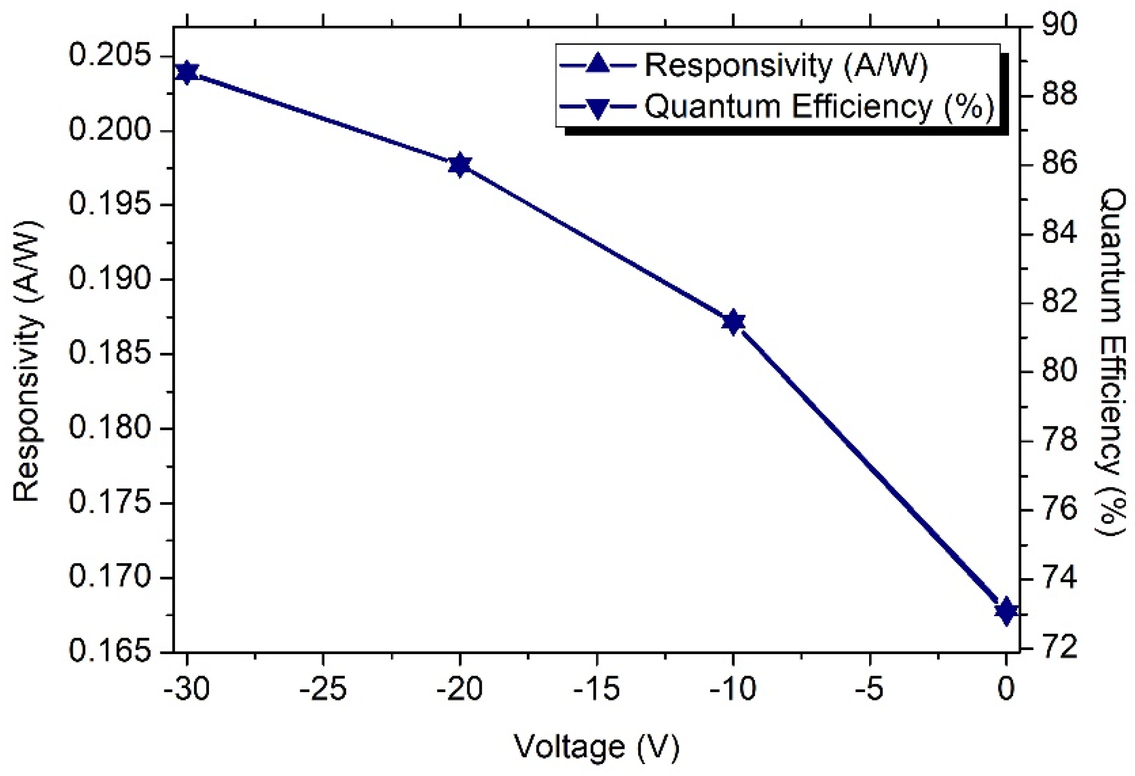
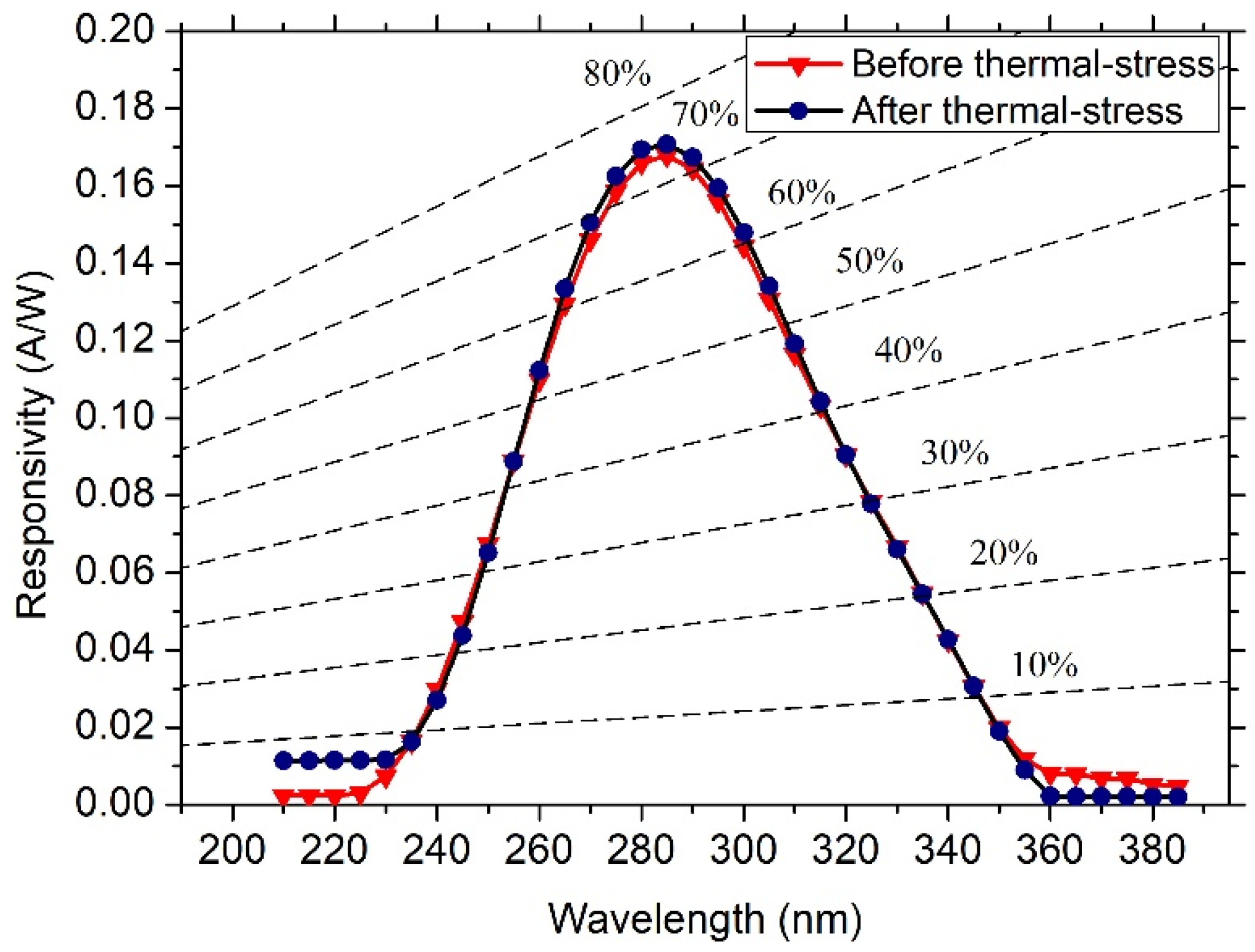
| [This work] | p-i-n | 0.168 0.204 | 0 −30 | 285 | 72.7 88.3 | 350 °C |
| Reverse Bias | Responsivity Peak (A/W) | Quantum Efficiency (%) |
|---|---|---|
| 0 V | 0.168 | 72.7 |
| 10 V | 0.187 | 81.1 |
| 20 V | 0.198 | 85.6 |
| 30 V | 0.204 | 88.3 |
Publisher’s Note: MDPI stays neutral with regard to jurisdictional claims in published maps and institutional affiliations. |
© 2021 by the authors. Licensee MDPI, Basel, Switzerland. This article is an open access article distributed under the terms and conditions of the Creative Commons Attribution (CC BY) license (https://creativecommons.org/licenses/by/4.0/).
Share and Cite
Megherbi, M.L.; Bencherif, H.; Dehimi, L.; Mallemace, E.D.; Rao, S.; Pezzimenti, F.; Della Corte, F.G. An Efficient 4H-SiC Photodiode for UV Sensing Applications. Electronics 2021, 10, 2517. https://doi.org/10.3390/electronics10202517
Megherbi ML, Bencherif H, Dehimi L, Mallemace ED, Rao S, Pezzimenti F, Della Corte FG. An Efficient 4H-SiC Photodiode for UV Sensing Applications. Electronics. 2021; 10(20):2517. https://doi.org/10.3390/electronics10202517
Chicago/Turabian StyleMegherbi, Mohamed L., Hichem Bencherif, Lakhdar Dehimi, Elisa D. Mallemace, Sandro Rao, Fortunato Pezzimenti, and Francesco G. Della Corte. 2021. "An Efficient 4H-SiC Photodiode for UV Sensing Applications" Electronics 10, no. 20: 2517. https://doi.org/10.3390/electronics10202517
APA StyleMegherbi, M. L., Bencherif, H., Dehimi, L., Mallemace, E. D., Rao, S., Pezzimenti, F., & Della Corte, F. G. (2021). An Efficient 4H-SiC Photodiode for UV Sensing Applications. Electronics, 10(20), 2517. https://doi.org/10.3390/electronics10202517