
Technique for Profiling the Cycling-Induced Oxide Trapped Charge in NAND Flash Memories


Abstract
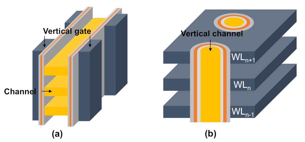
:1. Introduction
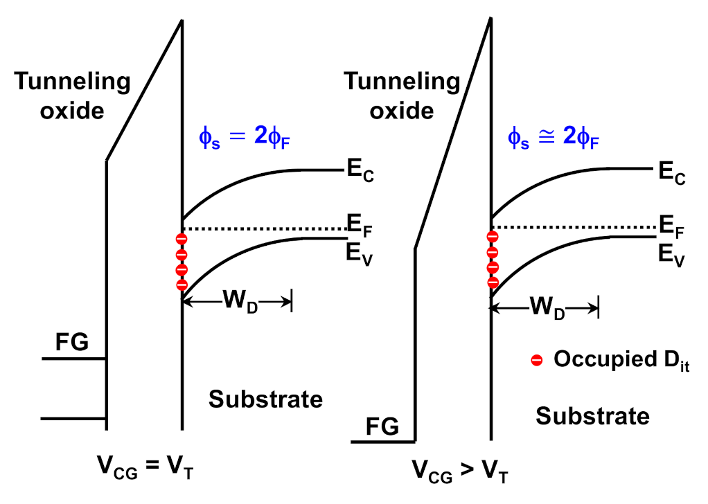
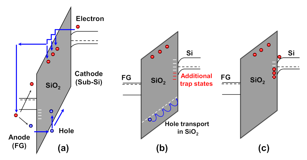
2. Shift in the Midgap Voltage
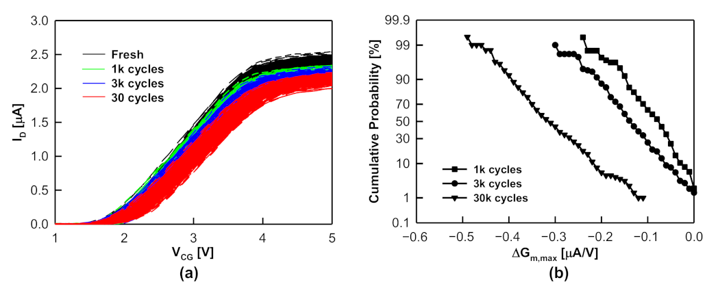
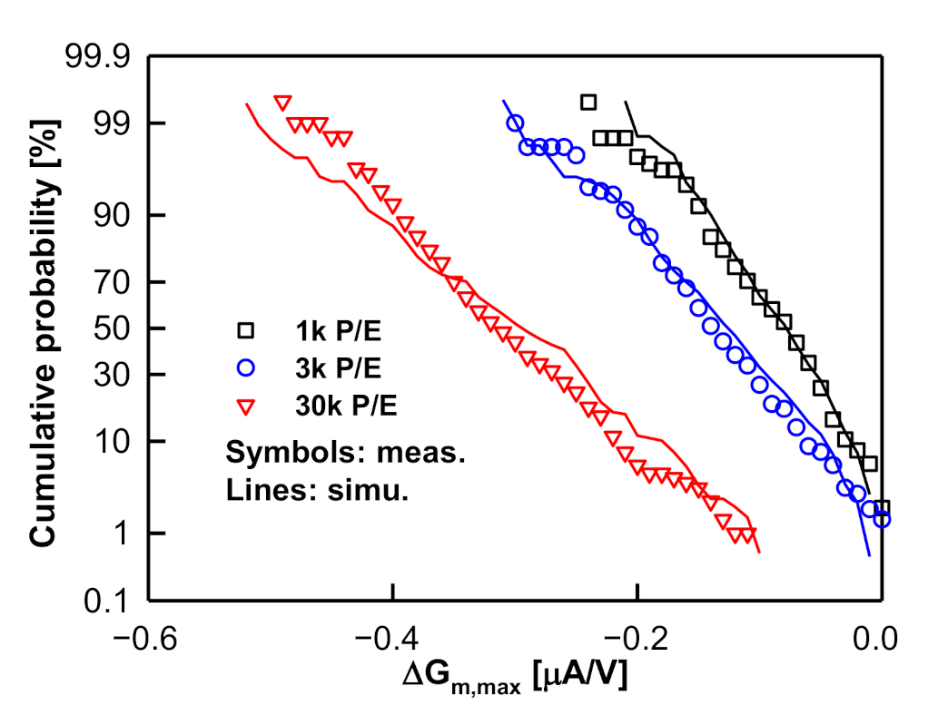
3. ∆Gm, max Statistics
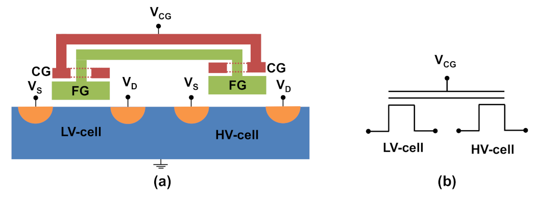
3.1. Experimental Setup
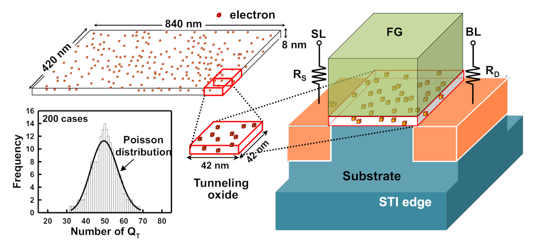
3.2. Simulation Methodology
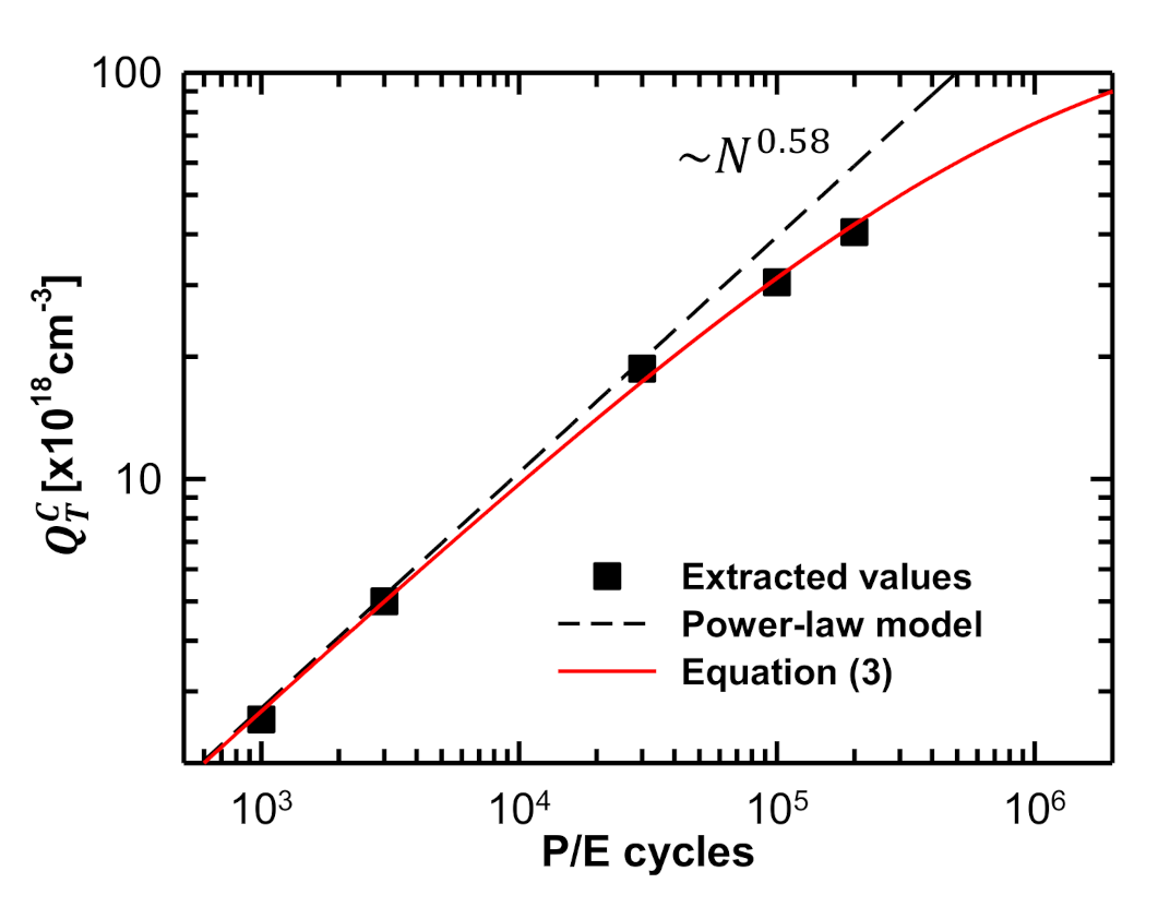
4. Endurance Characteristics
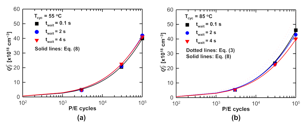
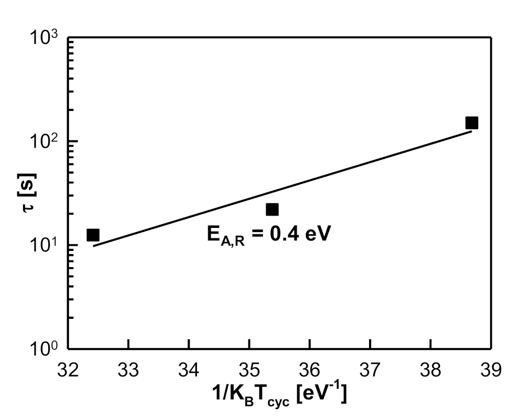
4.2. Endurance Degradation Model
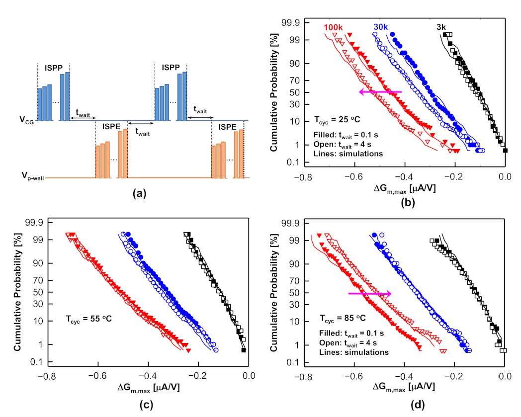
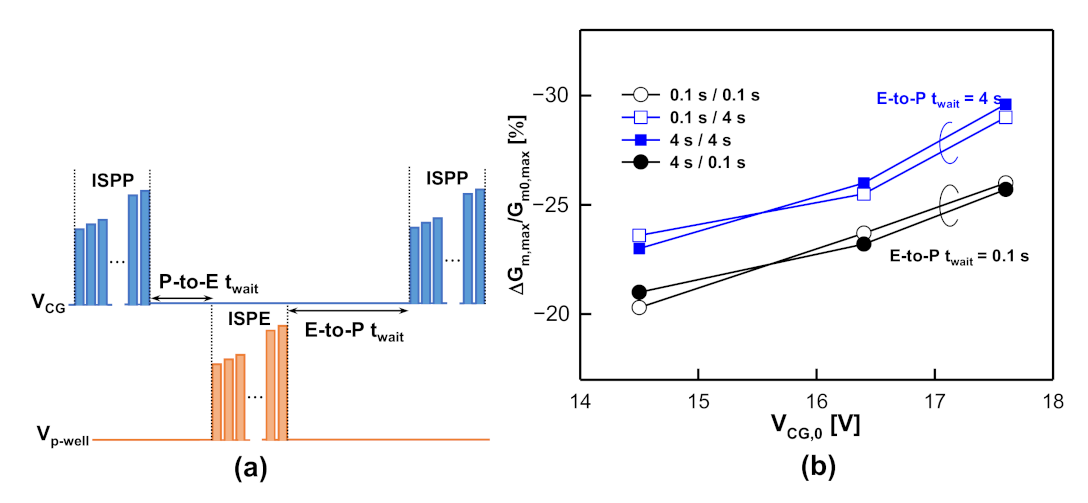
4.3. Effect of the Time Delay between P/E Cycles
5. Conclusions
Author Contributions
Funding
Acknowledgments
Conflicts of Interest
References
- Masuoka, F.; Momodomi, M.; Iwata, Y.; Shirota, R. New ultra high density EPROM and Flash EEPROM with NAND structure cell. In Proceedings of the 1987 International Electron Devices Meeting, New York, NY, USA, 6–9 December 1987; pp. 552–555. [Google Scholar]
- Shirota, R.; Itoh, Y.; Nakayama, R.; Momodomi, M.; Inoue, S.; Kirisawa, R.; Iwata, Y.; Chiba, M.; Masuoka, F. A new NAND cell for ultra high density 5 V-only EEPROMs. In Proceedings of the 1988 Symposium on VLSI Technology—Digest of Technical Papers, San Diego, CA, USA, 10–13 May 1988; pp. 33–34. [Google Scholar]
- Momodomi, M.; Kirisawa, R.; Nakayama, R.; Aritome, S.; Endoh, T.; Itoh, Y.; Iwata, Y.; Oodaira, H.; Tanaka, T.; Chiba, M.; et al. New device technologies for 5 Vonly 4 Mb EEPROM with NAND structure cell. In Proceedings of the 1988 International Electron Devices Meeting, San Francisco, CA, USA, 11–14 December 1988; pp. 412–415. [Google Scholar]
- Momodomi, M.; Itoh, Y.; Shirota, R.; Iwata, Y.; Nakayama, R.; Kirisawa, R.; Tanaka, T.; Aritome, S.; Endoh, T.; Ohuchi, K.; et al. An experimental 4-Mbit CMOS EEPROM with a NAND structure cell. IEEE J. Solid-State Circuits 1989, 24, 1238–1243. [Google Scholar] [CrossRef]
- Iwata, Y.; Momodomi, M.; Tanaka, T.; Oodaira, H.; Itoh, Y.; Nakayama, R.; Kirisawa, R.; Aritome, S.; Endoh, T.; Shirota, R.; et al. A high-density NAND EEPROM with block-page programming for microcomputer applications. IEEE J. Solid-State Circuits 1990, 25, 417–424. [Google Scholar] [CrossRef]
- Kirisawa, R.; Aritome, S.; Nakayama, R.; Endoh, T.; Shirota, R.; Masuoka, F. A NAND structured cell with a new programming technology for highly reliable SV-only Flash EEPROM. In Proceedings of the 1988 Symposium on VLSI Technology—Digest of Technical Papers, Honololu, HI, USA, 4–7 June 1990; pp. 129–130. [Google Scholar]
- Aritome, S.; Shirota, R.; Kirisawa, R.; Endoh, T.; Nakayama, N.; Sakui, K.; Masuoka, F. A reliable bi-polarity write/erase technology in flash EEPROMs. In Proceedings of the 1988 International Electron Devices Meeting, San Francisco, CA, USA, 9–12 December 1990; pp. 111–114. [Google Scholar]
- Micheloni, R.; Marelli, A.; Eshghi, K. Inside Solid State Drives (SSDs); Springer: New York, NY, USA, 2013. [Google Scholar]
- Spinelli, A.; Compagnoni, C.; Lacaita, A. Reliability of NAND Flash Memories: Planar Cells and Emerging Issues in 3D Devices. Computers 2017, 6, 16. [Google Scholar] [CrossRef]
- Ghetti, A.; Monzio Compagnoni, C.; Spinelli, A.S.; Visconti, A. Comprehensive analysis of random telegraph noise instability and its scaling in deca-nanometer Flash memories. IEEE Trans. Electron Devices 2009, 56, 1746–1752. [Google Scholar] [CrossRef]
- Kurata, H.; Otsuga, K.; Kotabe, A.; Kajiyama, S.; Osabe, T.; Sasago, Y.; Narumi, S.; Tokami, K.; Kamohara, S.; Tsuchiya, O. The impact of random telegraph signals on the scaling of multilevel Flash memories. In Proceedings of the 2006 Symposium on VLSI Technology (VLSI-Technology), Honolulu, HI, USA, 13–15 June 2006; pp. 112–113. [Google Scholar]
- Tega, N.; Miki, H.; Osabe, T.; Kotabe, A.; Otsuga, K.; Kurata, H.; Kamohara, S.; Tokami, K.; Ikeda, Y.; Yamada, R. Anomalously large threshold voltage fluctuation by complex random telegraph signal in floating gate Flash memory. In Proceedings of the 2006 International Electron Devices Meeting (IEDM), San Francisco, CA, USA, 11–13 December 2006; pp. 491–494. [Google Scholar]
- Resnati, D.; Nicosia, G.; Paolucci, G.M.; Visconti, A.; Monzio Compagnoni, C. Cycling-induced charge trapping/detrapping in Flash memories—Part I: Experimental evidence. IEEE Trans. Electron Devices 2016, 63, 4753–4760. [Google Scholar] [CrossRef]
- Mielke, N.; Belgal, H.; Kalastirsky, I.; Kalavade, P.; Kurtz, A.; Meng, Q.; Righos, N.; Wu, J. Flash EEPROM threshold instabilities due to charge trapping during program/erase cycling. IEEE Trans. Device Mater. Reliab. 2004, 4, 335–344. [Google Scholar] [CrossRef]
- Paolucci, G.M.; Monzio Compagnoni, C.; Miccoli, C.; Spinelli, A.S.; Lacaita, A.L.; Visconti, A. Revisiting charge trapping/detrapping in Flash memories from a discrete and statistical standpoint—Part I: VT instabilities. IEEE Trans. Electron Devices 2014, 61, 2802–2810. [Google Scholar] [CrossRef]
- Monzio Compagnoni, C.; Spinelli, A.S.; Gusmeroli, R.; Beltrami, S.; Ghetti, A.; Visconti, A. Ultimate accuracy for the NAND Flash program algorithm due to the electron injection statistics. IEEE Trans. Electron Devices 2008, 55, 2695–2702. [Google Scholar] [CrossRef]
- Monzio Compagnoni, C.; Gusmeroli, R.; Spinelli, A.S.; Visconti, A. Analytical model for the electron-injection statistics during programming of nanoscale NAND Flash memories. IEEE Trans. Electron Devices 2008, 55, 3192–3199. [Google Scholar] [CrossRef]
- Nishi, Y. (Ed.) Advances in Non-Volatile Memory and Storage Technology; Woodhead Publishing: Cambridge, UK, 2014. [Google Scholar]
- Lee, J.-D.; Hur, S.-H.; Choi, J.-D. Effects of floating-gate interference on NAND flash memory cell operation. IEEE Electron Device Lett. 2002, 23, 264–266. [Google Scholar]
- Goda, A.; Parat, K. Scaling directions for 2D and 3DNAND cells. In Proceedings of the 2012 IEEE International Electron Devices Meeting (IEDM), San Francisco, CA, USA, 10–13 December 2012. [Google Scholar]
- Goda, A. 3-D NAND technology achievements and future scaling perspectives. IEEE Trans. Electron Devices 2020, 67, 1373–1381. [Google Scholar] [CrossRef]
- Kim, W.; Choi, S.; Sung, J.; Lee, T.; Park, C.; Ko, H.; Jung, J.; Yoo, I.; Park, Y. Multi-layered vertical gate NAND Flash overcoming stacking limit for terabit density storage. In Proceedings of the 2009 Symposium on VLSI Technology, Kyoto, Japan, 15–17 June 2009; pp. 188–189. [Google Scholar]
- Tanaka, H.; Kido, M.; Yahashi., K.; Oomura, M.; Katsumata, R.; Kito, M.; Fukuzumi, Y.; Sato, M.; Nagata, Y.; Matsuoka, Y.; et al. Bit cost scalable technology with punch and plug process for ultra high density flash memory. In Proceedings of the 2007 Symposium on VLSI Technology, Kyoto, Japan, 12–14 June 2007; pp. 14–15. [Google Scholar]
- Fukuzumi, Y.; Katsumata, R.; Kito, M.; Kido, M.; Sato, M.; Tanaka, H.; Nagata, Y.; Matsuoka, Y.; Iwata, Y.; Aochi, H.; et al. Optimal integration and characteristics of vertical array devices for ultra-high density, bit-cost scalable flash memory. In Proceedings of the 2007 International Electron Devices Meeting (IEDM), Washington, DC, USA, 10–12 December 2007; pp. 449–452. [Google Scholar]
- Jang, J.; Kim, H.-S.; Cho, W.; Cho, H.; Kim, J.; Shim, S.I.; Jang, Y.; Jeong, J.-H.; Son, B.-K.; Kim, D.-W.; et al. Vertical cell array using TCAT (terabit cell array transistor) technology for ultra high density NAND flash memory. In Proceedings of the 2009 Symposium on VLSI Technology, Kyoto, Japan, 15–17 June 2009; pp. 192–193. [Google Scholar]
- Elliott, J.; Jung, E.S. Ushering in the 3D Memory Era with V-NAND. In Proceedings of the Flash Memory Summit, Santa Clara, CA, USA, 13–15 August 2013. [Google Scholar]
- Park, K.T.; Byeon, D.S.; Kim, D.H. A world’s first product of three-dimensional vertical NAND Flash memory and beyond. In Proceedings of the 2014 14th Annual Non-Volatile Memory Technology Symposium (NVMTS), Jeju Island, Korea, 27–29 October 2014; pp. 1–5. [Google Scholar]
- Park, K.T.; Nam, S.; Kim, D.; Kwak, P.; Lee, D.; Choi, Y.H.; Choi, M.H.; Kwak, D.H.; Kim, D.H.; Kim, M.S.; et al. Three-Dimensional 128 Gb MLC Vertical nand Flash Memory With 24-WL Stacked Layers and 50 MB/s High-Speed Programming. IEEE J. Solid State Circuit 2015, 50, 204–213. [Google Scholar] [CrossRef]
- Kang, D.; Kim, M.; Jeon, S.-C.; Jung, W.; Park, J.; Choo, G.; Shim, D.-K.; Kavala, A.; Kim, S.-B.; Kang, K.-M.; et al. A 512Gb 3-bit/cell 3D 6th-generation V-NAND flash memory with 82MB/s write throughput and 1.2Gb/s interface. In Proceedings of the 2019 IEEE International Solid-State Circuits Conference (ISSCC), San Francisco, CA, USA, 17–21 February 2019; pp. 216–218. [Google Scholar]
- Cho, J.; Chris Kang, D.; Park, J.; Nam, S.-W.; Song, J.-H.; Jung, B.-K.; Lyu, J.; Lee, H.; Kim, W.-T.; Jeon, H.; et al. A 512Gb 3b/Cell 7th-generation 3D-NAND flash memory with 184MB/s write throughput and 2.0Gb/s interface. In Proceedings of the 2021 IEEE International Solid-State Circuits Conference (ISSCC), San Francisco, CA, USA, 13–22 February 2021; pp. 426–428. [Google Scholar]
- Monzio Compagnoni, C.; Goda, A.; Spinelli, A.S.; Feeley, P.; Lacaita, A.L.; Visconti, A. Reviewing the evolution of the NAND Flash technology. Proc. IEEE 2017, 105, 1609–1633. [Google Scholar] [CrossRef]
- Fayrushin, A.; Lee, C.-H.; Park, Y.; Choi, J.-H.; Chung, C. Unified endurance degradation model of floating gate NAND flash memory. IEEE Trans. Electron Devices 2013, 60, 2031–2037. [Google Scholar] [CrossRef]
- Xia, Z.; Kim, D.S.; Jeong, N.; Kim, Y.-G.; Kim, J.-H.; Lee, K.-H.; Park, Y.-K.; Chung, C.; Lee, H.; Han, J. Comprehensive modeling of NAND flash memory reliability: Endurance and data retention. In Proceedings of the IEEE International Reliability Physics Symposium (IRPS), Anaheim, CA, USA, 15–19 April 2012; pp. MY.5.1–MY.5.4. [Google Scholar]
- Yang, B.-J.; Wu, Y.-T.; Chiu, Y.-Y.; Kuo, T.-M.; Chang, J.-H.; Wang, P.-Y.; Shirota, R. Evaluation of the role of deep trap state using analytical model in the program/erase cycling of NAND flash memory and its process dependence. IEEE Trans. Electron Devices 2018, 65, 499–506. [Google Scholar] [CrossRef]
- Watanabe, H.; Yao, K.; Lin, J. Numerical study of very small floating islands. IEEE Trans. Electron. Devices 2014, 61, 1145–1152. [Google Scholar] [CrossRef]
- Lin, P.-J.-J.; Lee, C.-A.-A.; Yao, C.-W.-K.; Lin, H.-J.-V.; Watanabe, H. Localized tunneling phenomena of nanometer scaled high-K gate-stack. IEEE Trans. Electron Devices 2017, 64, 3077–3083. [Google Scholar] [CrossRef]
- Shirota, R.; Yang, B.-J.; Chiu, Y.-Y.; Chen, H.-T.; Ng, S.-F.; Wang, P.-Y.; Chang, J.-H.; Kurachi, I. New accurate method to analyze both floating gate charge and tunnel oxide trapped charge profile in NAND flash memory. In Proceedings of the IEEE International Memory Workshop (IMW), Taipei, Taiwan, 18–21 May 2014; pp. 55–58. [Google Scholar]
- Shirota, R.; Yang, B.-J.; Chiu, Y.-Y.; Chen, H.-T.; Ng, S.-F.; Wang, P.-Y.; Chang, J.-H.; Kurachi, I. New method to analyze the shift of floating gate charge and generated tunnel oxide trapped charge profile in NAND flash memory by program/erase endurance. IEEE Trans. Electron Devices 2015, 62, 114–120. [Google Scholar] [CrossRef]
- Chiu, Y.-Y.; Lin, I.-C.; Chang, K.-C.; Yang, B.-J.; Takeshita, T.; Yano, M.; Shirota, R. Transconductance distribution in program/erase cycling of NAND flash memory devices: A Statistical Investigation. IEEE Trans. Electron Devices 2019, 66, 1255–1261. [Google Scholar] [CrossRef]
- Hemink, G.J.; Tanaka, T.; Endoh, T.; Aritome, S.; Shirota, R. Fast and accurate programming method for multi-level NAND EEPROMs. In Proceedings of the 1995 Symposium on VLSI Technology—Digest of Technical Papers, Kyoto, Japan, 6–8 June 1995; pp. 129–130. [Google Scholar]
- Joe, S.-M.; Yi, J.-H.; Park, S.-K.; Kwon, H.-I.; Lee, J.-H. Position–dependent threshold–voltage variation by random telegraph noise in NAND flash memory strings. IEEE Trans. Electron Devices 2010, 31, 635–637. [Google Scholar]
- van Langevelde, R.; Klaassen, F.M. An explicit surface-potentialbased MOSFET model for circuit simulation. Solid-State Electron. 2000, 44, 409–418. [Google Scholar] [CrossRef]
- Walters, M.; Reisman, A. Radiation-induced neutral electron trap generation in electrically biased insulated gate field effect transistor gate insulators. J. Electrochem. Soc. 1991, 138, 2756–2762. [Google Scholar] [CrossRef]
- Nicklaw, C.J.; Lu, Z.-Y.; Fleetwood, D.M.; Schrimpf, R.D.; Pantelides, S.T. The structure, properties, and dynamics of oxygen vacancies in amorphous SiO2. IEEE Trans. Nucl. Sci. 2002, 49, 2667–2673. [Google Scholar] [CrossRef]
- Satake, H.; Toriumi, A. Common origin for stress-induced leakage current and electron trap generation in SiO2. Appl. Phys. Lett. 1995, 67, 3489–3490. [Google Scholar] [CrossRef]
- DiMaria, D.J.; Stasiak, J.W. Trap creation in silicon dioxide produced by hot electrons. J. Appl. Phys. 1989, 65, 2342–2356. [Google Scholar] [CrossRef]
- Chiu, Y.-Y.; Chang, K.-C.; Lin, H.-J.; Tsai, H.-T.-E.; Lin, P.-J.; Li, H.-C.; Takeshita, T.; Yano, M.; Shirota, R. Impact of program/erase Cycling Interval on the transconductance distribution of NAND flash memory devices. IEEE Trans. Electron Devices 2020, 67, 4897–4903. [Google Scholar] [CrossRef]
- Shirota, R.; Yang, B.-J.; Chiu, Y.-Y.; Wu, Y.-T.; Wang, P.-Y.; Chang, J.-H.; Yano, M.; Aoki, M.; Takeshita, T.; Wang, P.-Y.; et al. Improvement of oxide reliability in NAND flash memories using tight endurance cycling with shorter idling period. In Proceedings of the IEEE International Reliability Physics Symposium (IRPS), Monterey, CA, USA, 19–23 April 2015; pp. MY.12.1–MY.12.5. [Google Scholar]
- Miccoli, C.; Monzio Compagnoni, C.; Beltrami, S.; Spinelli, A.S.; Visconti, A. Threshold-voltage instability due to damage recovery in nanoscale NAND flash memories. IEEE Trans. Electron Devices 2011, 58, 2406–2414. [Google Scholar] [CrossRef]
- Lee, M.C.; Wong, H.Y. Investigation on the impact of program/erase cycling frequency on data retention of nanoscale charge trap nonvolatile memory. IEEE Electron Device Lett. 2014, 35, 918–920. [Google Scholar]
- Mielke, N.; Belgal, H.P.; Fazio, A.; Meng, Q.; Righos, N. Recovery effects in the distributed cycling of flash memories. In Proceedings of the IEEE International Reliability Physics Symposium (IRPS), San Jose, CA, USA, 26–30 March 2006; pp. 29–35. [Google Scholar]
- Wang, Y.; White, M.H. An analytical retention model for SONOS nonvolatile memory devices in the excess electron state. Solid-State Electron. 2005, 49, 97–107. [Google Scholar] [CrossRef]
- Chiu, Y.-Y.; Yang, L.F.-H.; Chang, R.-W.; Sun, W.-T.; Lo, C.-Y.; Hsu, C.-J.; Kuo, C.-W.; Shirota, R. Characterization of the charge trapping properties in pchannel silicon–oxide–nitride–oxide–silicon memory devices including SiO2/Si3N4 interfacial transition layer. Jpn. J. Appl. Phys. 2015, 54, 104201.1–104201.6. [Google Scholar] [CrossRef]
- Thompson, S.E.; Nishida, T. Tunneling and thermal emission of electrons from a distribution of shallow traps in SiO2. Appl. Phys. Lett. 1991, 58, 1262–1264. [Google Scholar] [CrossRef]
- Chiu, Y.-Y.; Tsai, H.-T.-E.; Chang, K.-C.; Kumari, R.; Li, H.-C.; Takeshita, T.; Yano, M.; Shirota, R. The origin of oxide degradation during time interval between program/erase cycles in NAND Flash memory devices. Jpn. J. Appl. Phys. 2021, 60, 074004.1–074004.5. [Google Scholar] [CrossRef]
- Lai, S.K. Interface trap generation in silicon dioxide when electrons are captured by trapped holes. J. Appl. Phys. 1983, 54, 2540–2546. [Google Scholar] [CrossRef]


Publisher’s Note: MDPI stays neutral with regard to jurisdictional claims in published maps and institutional affiliations. |
© 2021 by the authors. Licensee MDPI, Basel, Switzerland. This article is an open access article distributed under the terms and conditions of the Creative Commons Attribution (CC BY) license (https://creativecommons.org/licenses/by/4.0/).
Share and Cite
Chiu, Y.-Y.; Shirota, R. Technique for Profiling the Cycling-Induced Oxide Trapped Charge in NAND Flash Memories. Electronics 2021, 10, 2492. https://doi.org/10.3390/electronics10202492
Chiu Y-Y, Shirota R. Technique for Profiling the Cycling-Induced Oxide Trapped Charge in NAND Flash Memories. Electronics. 2021; 10(20):2492. https://doi.org/10.3390/electronics10202492
Chicago/Turabian StyleChiu, Yung-Yueh, and Riichiro Shirota. 2021. "Technique for Profiling the Cycling-Induced Oxide Trapped Charge in NAND Flash Memories" Electronics 10, no. 20: 2492. https://doi.org/10.3390/electronics10202492
APA StyleChiu, Y.-Y., & Shirota, R. (2021). Technique for Profiling the Cycling-Induced Oxide Trapped Charge in NAND Flash Memories. Electronics, 10(20), 2492. https://doi.org/10.3390/electronics10202492